CD4040BM96E4中文资料
CD4001BM96G4中文资料

Data sheet acquired from Harris Semiconductor SCHS015C – Revised August 2003The CD4001B, CD4002B, and CD4025B types are supplied in 14-lead hermetic dual-in-line ceramic packages (F3A suffix), 14-lead dual-in-line plastic packages (E suffix), 14-lead small-outline packages (M, MT, M96, and NSR suffixes), and 14-lead thin shrink small-outline packages (PW and PWR suffixes).IMPORTANT NOTICETexas Instruments Incorporated and its subsidiaries(TI)reserve the right to make corrections,modifications,enhancements, improvements,and other changes to its products and services at any time and to discontinue any product or service without notice. Customers should obtain the latest relevant information before placing orders and should verify that such information is current and complete.All products are sold subject to TI’s terms and conditions of sale supplied at the time of order acknowledgment.TI warrants performance of its hardware products to the specifications applicable at the time of sale in accordance with TI’s standard warranty.Testing and other quality control techniques are used to the extent TI deems necessary to support this warranty.Except where mandated by government requirements,testing of all parameters of each product is not necessarily performed.TI assumes no liability for applications assistance or customer product design.Customers are responsible for their products and applications using TI components.To minimize the risks associated with customer products and applications,customers should provide adequate design and operating safeguards.TI does not warrant or represent that any license,either express or implied,is granted under any TI patent right,copyright,mask work right,or other TI intellectual property right relating to any combination,machine,or process in which TI products or services are rmation published by TI regarding third-party products or services does not constitute a license from TI to use such products or services or a warranty or endorsement e of such information may require a license from a third party under the patents or other intellectual property of the third party,or a license from TI under the patents or other intellectual property of TI. Reproduction of information in TI data books or data sheets is permissible only if reproduction is without alteration and is accompanied by all associated warranties,conditions,limitations,and notices.Reproduction of this information with alteration is an unfair and deceptive business practice.TI is not responsible or liable for such altered documentation.Resale of TI products or services with statements different from or beyond the parameters stated by TI for that product or service voids all express and any implied warranties for the associated TI product or service and is an unfair and deceptive business practice.TI is not responsible or liable for any such statements.TI products are not authorized for use in safety-critical applications(such as life support)where a failure of the TI product would reasonably be expected to cause severe personal injury or death,unless officers of the parties have executed an agreement specifically governing such use.Buyers represent that they have all necessary expertise in the safety and regulatory ramifications of their applications,and acknowledge and agree that they are solely responsible for all legal,regulatory and safety-related requirements concerning their products and any use of TI products in such safety-critical applications,notwithstanding any applications-related information or support that may be provided by TI.Further,Buyers must fully indemnify TI and its representatives against any damages arising out of the use of TI products in such safety-critical applications.TI products are neither designed nor intended for use in military/aerospace applications or environments unless the TI products are specifically designated by TI as military-grade or"enhanced plastic."Only products designated by TI as military-grade meet military specifications.Buyers acknowledge and agree that any such use of TI products which TI has not designated as military-grade is solely at the Buyer's risk,and that they are solely responsible for compliance with all legal and regulatory requirements in connection with such use.TI products are neither designed nor intended for use in automotive applications or environments unless the specific TI products are designated by TI as compliant with ISO/TS16949requirements.Buyers acknowledge and agree that,if they use anynon-designated products in automotive applications,TI will not be responsible for any failure to meet such requirements. Following are URLs where you can obtain information on other Texas Instruments products and application solutions:Products ApplicationsAmplifiers AudioData Converters AutomotiveDSP BroadbandInterface Digital ControlLogic MilitaryPower Mgmt Optical NetworkingMicrocontrollers SecurityLow Power TelephonyWirelessVideo&ImagingWirelessMailing Address:Texas Instruments,Post Office Box655303,Dallas,Texas75265Copyright©2007,Texas Instruments IncorporatedPACKAGING INFORMATIONOrderable Device Status(1)PackageType PackageDrawingPins PackageQtyEco Plan(2)Lead/Ball Finish MSL Peak Temp(3)7704403CA ACTIVE CDIP J141TBD A42SNPB N/A for Pkg Type 89263AKB3T OBSOLETE CFP WR16TBD Call TI Call TICD4001BE ACTIVE PDIP N1425Pb-Free(RoHS)CU NIPDAU N/A for Pkg TypeCD4001BEE4ACTIVE PDIP N1425Pb-Free(RoHS)CU NIPDAU N/A for Pkg Type CD4001BF ACTIVE CDIP J141TBD A42SNPB N/A for Pkg Type CD4001BF3A ACTIVE CDIP J141TBD A42SNPB N/A for Pkg Type CD4001BF3AS2534OBSOLETE CDIP J14TBD Call TI Call TI CD4001BM ACTIVE SOIC D1450Green(RoHS&no Sb/Br)CU NIPDAU Level-1-260C-UNLIMCD4001BM96ACTIVE SOIC D142500Green(RoHS&no Sb/Br)CU NIPDAU Level-1-260C-UNLIMCD4001BM96E4ACTIVE SOIC D142500Green(RoHS&no Sb/Br)CU NIPDAU Level-1-260C-UNLIMCD4001BM96G4ACTIVE SOIC D142500Green(RoHS&no Sb/Br)CU NIPDAU Level-1-260C-UNLIMCD4001BME4ACTIVE SOIC D1450Green(RoHS&no Sb/Br)CU NIPDAU Level-1-260C-UNLIMCD4001BMG4ACTIVE SOIC D1450Green(RoHS&no Sb/Br)CU NIPDAU Level-1-260C-UNLIMCD4001BMT ACTIVE SOIC D14250Green(RoHS&no Sb/Br)CU NIPDAU Level-1-260C-UNLIMCD4001BMTE4ACTIVE SOIC D14250Green(RoHS&no Sb/Br)CU NIPDAU Level-1-260C-UNLIMCD4001BMTG4ACTIVE SOIC D14250Green(RoHS&no Sb/Br)CU NIPDAU Level-1-260C-UNLIMCD4001BNSR ACTIVE SO NS142000Green(RoHS&no Sb/Br)CU NIPDAU Level-1-260C-UNLIMCD4001BNSRE4ACTIVE SO NS142000Green(RoHS&no Sb/Br)CU NIPDAU Level-1-260C-UNLIMCD4001BNSRG4ACTIVE SO NS142000Green(RoHS&no Sb/Br)CU NIPDAU Level-1-260C-UNLIMCD4001BPW ACTIVE TSSOP PW1490Green(RoHS&no Sb/Br)CU NIPDAU Level-1-260C-UNLIMCD4001BPWE4ACTIVE TSSOP PW1490Green(RoHS&no Sb/Br)CU NIPDAU Level-1-260C-UNLIMCD4001BPWG4ACTIVE TSSOP PW1490Green(RoHS&no Sb/Br)CU NIPDAU Level-1-260C-UNLIMCD4001BPWR ACTIVE TSSOP PW142000Green(RoHS&no Sb/Br)CU NIPDAU Level-1-260C-UNLIMCD4001BPWRE4ACTIVE TSSOP PW142000Green(RoHS&no Sb/Br)CU NIPDAU Level-1-260C-UNLIMCD4001BPWRG4ACTIVE TSSOP PW142000Green(RoHS&no Sb/Br)CU NIPDAU Level-1-260C-UNLIMCD4002BE ACTIVE PDIP N1425Pb-Free(RoHS)CU NIPDAU N/A for Pkg TypeCD4002BEE4ACTIVE PDIP N1425Pb-Free(RoHS)CU NIPDAU N/A for Pkg TypeOrderable Device Status(1)PackageType PackageDrawingPins PackageQtyEco Plan(2)Lead/Ball Finish MSL Peak Temp(3)CD4002BF ACTIVE CDIP J141TBD A42SNPB N/A for Pkg Type CD4002BF3A ACTIVE CDIP J141TBD A42SNPB N/A for Pkg Type CD4002BM ACTIVE SOIC D1450Green(RoHS&no Sb/Br)CU NIPDAU Level-1-260C-UNLIMCD4002BM96ACTIVE SOIC D142500Green(RoHS&no Sb/Br)CU NIPDAU Level-1-260C-UNLIMCD4002BM96E4ACTIVE SOIC D142500Green(RoHS&no Sb/Br)CU NIPDAU Level-1-260C-UNLIMCD4002BM96G4ACTIVE SOIC D142500Green(RoHS&no Sb/Br)CU NIPDAU Level-1-260C-UNLIMCD4002BME4ACTIVE SOIC D1450Green(RoHS&no Sb/Br)CU NIPDAU Level-1-260C-UNLIMCD4002BMG4ACTIVE SOIC D1450Green(RoHS&no Sb/Br)CU NIPDAU Level-1-260C-UNLIMCD4002BMT ACTIVE SOIC D14250Green(RoHS&no Sb/Br)CU NIPDAU Level-1-260C-UNLIMCD4002BMTE4ACTIVE SOIC D14250Green(RoHS&no Sb/Br)CU NIPDAU Level-1-260C-UNLIMCD4002BMTG4ACTIVE SOIC D14250Green(RoHS&no Sb/Br)CU NIPDAU Level-1-260C-UNLIMCD4002BNSR ACTIVE SO NS142000Green(RoHS&no Sb/Br)CU NIPDAU Level-1-260C-UNLIMCD4002BNSRE4ACTIVE SO NS142000Green(RoHS&no Sb/Br)CU NIPDAU Level-1-260C-UNLIMCD4002BNSRG4ACTIVE SO NS142000Green(RoHS&no Sb/Br)CU NIPDAU Level-1-260C-UNLIMCD4002BPW ACTIVE TSSOP PW1490Green(RoHS&no Sb/Br)CU NIPDAU Level-1-260C-UNLIMCD4002BPWE4ACTIVE TSSOP PW1490Green(RoHS&no Sb/Br)CU NIPDAU Level-1-260C-UNLIMCD4002BPWG4ACTIVE TSSOP PW1490Green(RoHS&no Sb/Br)CU NIPDAU Level-1-260C-UNLIMCD4002BPWR ACTIVE TSSOP PW142000Green(RoHS&no Sb/Br)CU NIPDAU Level-1-260C-UNLIMCD4002BPWRE4ACTIVE TSSOP PW142000Green(RoHS&no Sb/Br)CU NIPDAU Level-1-260C-UNLIMCD4002BPWRG4ACTIVE TSSOP PW142000Green(RoHS&no Sb/Br)CU NIPDAU Level-1-260C-UNLIMCD4025BE ACTIVE PDIP N1425Pb-Free(RoHS)CU NIPDAU N/A for Pkg TypeCD4025BEE4ACTIVE PDIP N1425Pb-Free(RoHS)CU NIPDAU N/A for Pkg TypeCD4025BF ACTIVE CDIP J141TBD A42SNPB N/A for Pkg Type CD4025BF3A ACTIVE CDIP J141TBD A42SNPB N/A for Pkg Type CD4025BM ACTIVE SOIC D1450Green(RoHS&no Sb/Br)CU NIPDAU Level-1-260C-UNLIMCD4025BM96ACTIVE SOIC D142500Green(RoHS&no Sb/Br)CU NIPDAU Level-1-260C-UNLIMCD4025BM96E4ACTIVE SOIC D142500Green(RoHS&no Sb/Br)CU NIPDAU Level-1-260C-UNLIMCD4025BM96G4ACTIVE SOIC D142500Green(RoHS&CU NIPDAU Level-1-260C-UNLIMOrderable Device Status(1)PackageType PackageDrawingPins PackageQtyEco Plan(2)Lead/Ball Finish MSL Peak Temp(3)no Sb/Br)CD4025BME4ACTIVE SOIC D1450Green(RoHS&no Sb/Br)CU NIPDAU Level-1-260C-UNLIMCD4025BMG4ACTIVE SOIC D1450Green(RoHS&no Sb/Br)CU NIPDAU Level-1-260C-UNLIMCD4025BMT ACTIVE SOIC D14250Green(RoHS&no Sb/Br)CU NIPDAU Level-1-260C-UNLIMCD4025BMTE4ACTIVE SOIC D14250Green(RoHS&no Sb/Br)CU NIPDAU Level-1-260C-UNLIMCD4025BMTG4ACTIVE SOIC D14250Green(RoHS&no Sb/Br)CU NIPDAU Level-1-260C-UNLIMCD4025BNSR ACTIVE SO NS142000Green(RoHS&no Sb/Br)CU NIPDAU Level-1-260C-UNLIMCD4025BNSRE4ACTIVE SO NS142000Green(RoHS&no Sb/Br)CU NIPDAU Level-1-260C-UNLIMCD4025BNSRG4ACTIVE SO NS142000Green(RoHS&no Sb/Br)CU NIPDAU Level-1-260C-UNLIMCD4025BPW ACTIVE TSSOP PW1490Green(RoHS&no Sb/Br)CU NIPDAU Level-1-260C-UNLIMCD4025BPWE4ACTIVE TSSOP PW1490Green(RoHS&no Sb/Br)CU NIPDAU Level-1-260C-UNLIMCD4025BPWG4ACTIVE TSSOP PW1490Green(RoHS&no Sb/Br)CU NIPDAU Level-1-260C-UNLIMCD4025BPWR ACTIVE TSSOP PW142000Green(RoHS&no Sb/Br)CU NIPDAU Level-1-260C-UNLIMCD4025BPWRE4ACTIVE TSSOP PW142000Green(RoHS&no Sb/Br)CU NIPDAU Level-1-260C-UNLIMCD4025BPWRG4ACTIVE TSSOP PW142000Green(RoHS&no Sb/Br)CU NIPDAU Level-1-260C-UNLIM JM38510/05252BCA ACTIVE CDIP J141TBD A42SNPB N/A for Pkg Type JM38510/05254BCA ACTIVE CDIP J141TBD A42SNPB N/A for Pkg Type (1)The marketing status values are defined as follows:ACTIVE:Product device recommended for new designs.LIFEBUY:TI has announced that the device will be discontinued,and a lifetime-buy period is in effect.NRND:Not recommended for new designs.Device is in production to support existing customers,but TI does not recommend using this part in a new design.PREVIEW:Device has been announced but is not in production.Samples may or may not be available.OBSOLETE:TI has discontinued the production of the device.(2)Eco Plan-The planned eco-friendly classification:Pb-Free(RoHS),Pb-Free(RoHS Exempt),or Green(RoHS&no Sb/Br)-please check /productcontent for the latest availability information and additional product content details.TBD:The Pb-Free/Green conversion plan has not been defined.Pb-Free(RoHS):TI's terms"Lead-Free"or"Pb-Free"mean semiconductor products that are compatible with the current RoHS requirements for all6substances,including the requirement that lead not exceed0.1%by weight in homogeneous materials.Where designed to be soldered at high temperatures,TI Pb-Free products are suitable for use in specified lead-free processes.Pb-Free(RoHS Exempt):This component has a RoHS exemption for either1)lead-based flip-chip solder bumps used between the die and package,or2)lead-based die adhesive used between the die and leadframe.The component is otherwise considered Pb-Free(RoHS compatible)as defined above.Green(RoHS&no Sb/Br):TI defines"Green"to mean Pb-Free(RoHS compatible),and free of Bromine(Br)and Antimony(Sb)based flame retardants(Br or Sb do not exceed0.1%by weight in homogeneous material)(3)MSL,Peak Temp.--The Moisture Sensitivity Level rating according to the JEDEC industry standard classifications,and peak solder temperature.Important Information and Disclaimer:The information provided on this page represents TI's knowledge and belief as of the date that it is provided.TI bases its knowledge and belief on information provided by third parties,and makes no representation or warranty as to the accuracy of such information.Efforts are underway to better integrate information from third parties.TI has taken and continues to take reasonable steps to provide representative and accurate information but may not have conducted destructive testing or chemical analysis on incoming materials and chemicals.TI and TI suppliers consider certain information to be proprietary,and thus CAS numbers and other limited information may not be available for release.In no event shall TI's liability arising out of such information exceed the total purchase price of the TI part(s)at issue in this document sold by TI to Customer on an annual basis.TAPE AND REELINFORMATION*Alldimensions are nominalDevicePackage Type Package Drawing Pins SPQReel Diameter (mm)Reel Width W1(mm)A0(mm)B0(mm)K0(mm)P1(mm)W (mm)Pin1Quadrant CD4001BM96SOIC D 142500330.016.4 6.59.0 2.18.016.0Q1CD4001BNSR SO NS 142000330.016.48.210.5 2.512.016.0Q1CD4001BPWR TSSOP PW 142000330.012.47.0 5.6 1.68.012.0Q1CD4002BM96SOIC D 142500330.016.4 6.59.0 2.18.016.0Q1CD4002BNSR SO NS 142000330.016.48.210.5 2.512.016.0Q1CD4002BPWR TSSOP PW 142000330.012.47.0 5.6 1.68.012.0Q1CD4025BM96SOIC D 142500330.016.4 6.59.0 2.18.016.0Q1CD4025BNSR SO NS 142000330.016.48.210.5 2.512.016.0Q1CD4025BPWRTSSOPPW142000330.012.47.05.61.68.012.0Q1PACKAGE MATERIALS INFORMATION11-Mar-2008*Alldimensions are nominalDevice Package TypePackage DrawingPins SPQ Length (mm)Width (mm)Height (mm)CD4001BM96SOIC D 142500346.0346.033.0CD4001BNSR SO NS 142000346.0346.033.0CD4001BPWR TSSOP PW 142000346.0346.029.0CD4002BM96SOIC D 142500346.0346.033.0CD4002BNSR SO NS 142000346.0346.033.0CD4002BPWR TSSOP PW 142000346.0346.029.0CD4025BM96SOIC D 142500346.0346.033.0CD4025BNSR SO NS 142000346.0346.033.0CD4025BPWRTSSOPPW142000346.0346.029.0PACKAGE MATERIALS INFORMATION11-Mar-2008。
CD40192BE,CD40193BE,CD40193BPWRE4,CD40193BPWRG4,CD40192BNSRE4,CD40193BNSRE4, 规格书,Datasheet 资料

Data sheet acquired from Harris SemiconductorSCHS106B – Revised July 2003The CD40192B and CD40193B types aresupplied in 16-lead hermetic dual-in-lineceramic packages (F3A suffix), 16-leaddual-in-line plastic packages (E suffix),16-lead small-outline packages (NSR suffix),and 16-lead thin shrink small-outlinepackages (PW and PWR suffixes).Copyright 2003, Texas Instruments IncorporatedPACKAGING INFORMATIONOrderable Device Status(1)PackageType PackageDrawingPins PackageQtyEco Plan(2)Lead/Ball Finish MSL Peak Temp(3)CD40192BE ACTIVE PDIP N1625Pb-Free(RoHS)CU NIPDAU N/A for Pkg TypeCD40192BEE4ACTIVE PDIP N1625Pb-Free(RoHS)CU NIPDAU N/A for Pkg Type CD40192BF ACTIVE CDIP J161TBD A42N/A for Pkg Type CD40192BF3A ACTIVE CDIP J161TBD A42N/A for Pkg Type CD40192BNSR ACTIVE SO NS162000Green(RoHS&no Sb/Br)CU NIPDAU Level-1-260C-UNLIMCD40192BNSRE4ACTIVE SO NS162000Green(RoHS&no Sb/Br)CU NIPDAU Level-1-260C-UNLIMCD40192BNSRG4ACTIVE SO NS162000Green(RoHS&no Sb/Br)CU NIPDAU Level-1-260C-UNLIMCD40193BE ACTIVE PDIP N1625Pb-Free(RoHS)CU NIPDAU N/A for Pkg TypeCD40193BEE4ACTIVE PDIP N1625Pb-Free(RoHS)CU NIPDAU N/A for Pkg Type CD40193BF3A ACTIVE CDIP J161TBD A42N/A for Pkg Type CD40193BNSR ACTIVE SO NS162000Green(RoHS&no Sb/Br)CU NIPDAU Level-1-260C-UNLIMCD40193BNSRE4ACTIVE SO NS162000Green(RoHS&no Sb/Br)CU NIPDAU Level-1-260C-UNLIMCD40193BNSRG4ACTIVE SO NS162000Green(RoHS&no Sb/Br)CU NIPDAU Level-1-260C-UNLIMCD40193BPW ACTIVE TSSOP PW1690Green(RoHS&no Sb/Br)CU NIPDAU Level-1-260C-UNLIMCD40193BPWE4ACTIVE TSSOP PW1690Green(RoHS&no Sb/Br)CU NIPDAU Level-1-260C-UNLIMCD40193BPWG4ACTIVE TSSOP PW1690Green(RoHS&no Sb/Br)CU NIPDAU Level-1-260C-UNLIMCD40193BPWR ACTIVE TSSOP PW162000Green(RoHS&no Sb/Br)CU NIPDAU Level-1-260C-UNLIMCD40193BPWRE4ACTIVE TSSOP PW162000Green(RoHS&no Sb/Br)CU NIPDAU Level-1-260C-UNLIMCD40193BPWRG4ACTIVE TSSOP PW162000Green(RoHS&no Sb/Br)CU NIPDAU Level-1-260C-UNLIM(1)The marketing status values are defined as follows:ACTIVE:Product device recommended for new designs.LIFEBUY:TI has announced that the device will be discontinued,and a lifetime-buy period is in effect.NRND:Not recommended for new designs.Device is in production to support existing customers,but TI does not recommend using this part in a new design.PREVIEW:Device has been announced but is not in production.Samples may or may not be available.OBSOLETE:TI has discontinued the production of the device.(2)Eco Plan-The planned eco-friendly classification:Pb-Free(RoHS),Pb-Free(RoHS Exempt),or Green(RoHS&no Sb/Br)-please check /productcontent for the latest availability information and additional product content details.TBD:The Pb-Free/Green conversion plan has not been defined.Pb-Free(RoHS):TI's terms"Lead-Free"or"Pb-Free"mean semiconductor products that are compatible with the current RoHS requirements for all6substances,including the requirement that lead not exceed0.1%by weight in homogeneous materials.Where designed to be soldered at high temperatures,TI Pb-Free products are suitable for use in specified lead-free processes.Pb-Free(RoHS Exempt):This component has a RoHS exemption for either1)lead-based flip-chip solder bumps used between the die and package,or2)lead-based die adhesive used between the die and leadframe.The component is otherwise considered Pb-Free(RoHScompatible)as defined above.Green(RoHS&no Sb/Br):TI defines"Green"to mean Pb-Free(RoHS compatible),and free of Bromine(Br)and Antimony(Sb)based flame retardants(Br or Sb do not exceed0.1%by weight in homogeneous material)(3)MSL,Peak Temp.--The Moisture Sensitivity Level rating according to the JEDEC industry standard classifications,and peak solder temperature.Important Information and Disclaimer:The information provided on this page represents TI's knowledge and belief as of the date that it is provided.TI bases its knowledge and belief on information provided by third parties,and makes no representation or warranty as to the accuracy of such information.Efforts are underway to better integrate information from third parties.TI has taken and continues to take reasonable steps to provide representative and accurate information but may not have conducted destructive testing or chemical analysis on incoming materials and chemicals.TI and TI suppliers consider certain information to be proprietary,and thus CAS numbers and other limited information may not be available for release.In no event shall TI's liability arising out of such information exceed the total purchase price of the TI part(s)at issue in this document sold by TI to Customer on an annual basis.TAPE AND REEL INFORMATION*All dimensions are nominalDevicePackage Type Package Drawing Pins SPQReel Diameter (mm)Reel Width W1(mm)A0(mm)B0(mm)K0(mm)P1(mm)W (mm)Pin1Quadrant CD40192BNSR SO NS 162000330.016.48.210.5 2.512.016.0Q1CD40193BNSR SO NS 162000330.016.48.210.5 2.512.016.0Q1CD40193BPWRTSSOPPW162000330.012.46.95.61.68.012.0Q1*All dimensions are nominalDevice Package Type Package Drawing Pins SPQ Length(mm)Width(mm)Height(mm) CD40192BNSR SO NS162000367.0367.038.0 CD40193BNSR SO NS162000367.0367.038.0CD40193BPWR TSSOP PW162000367.0367.035.0IMPORTANT NOTICETexas Instruments Incorporated and its subsidiaries(TI)reserve the right to make corrections,enhancements,improvements and other changes to its semiconductor products and services per JESD46C and to discontinue any product or service per JESD48B.Buyers should obtain the latest relevant information before placing orders and should verify that such information is current and complete.All semiconductor products(also referred to herein as“components”)are sold subject to TI’s terms and conditions of sale supplied at the time of order acknowledgment.TI warrants performance of its components to the specifications applicable at the time of sale,in accordance with the warranty in TI’s terms and conditions of sale of semiconductor products.Testing and other quality control techniques are used to the extent TI deems necessary to support this warranty.Except where mandated by applicable law,testing of all parameters of each component is not necessarily performed.TI assumes no liability for applications assistance or the design of Buyers’products.Buyers are responsible for their products and applications using TI components.To minimize the risks associated with Buyers’products and applications,Buyers should provide adequate design and operating safeguards.TI does not warrant or represent that any license,either express or implied,is granted under any patent right,copyright,mask work right,or other intellectual property right relating to any combination,machine,or process in which TI components or services are rmation published by TI regarding third-party products or services does not constitute a license to use such products or services or a warranty or endorsement e of such information may require a license from a third party under the patents or other intellectual property of the third party,or a license from TI under the patents or other intellectual property of TI.Reproduction of significant portions of TI information in TI data books or data sheets is permissible only if reproduction is without alteration and is accompanied by all associated warranties,conditions,limitations,and notices.TI is not responsible or liable for such altered rmation of third parties may be subject to additional restrictions.Resale of TI components or services with statements different from or beyond the parameters stated by TI for that component or service voids all express and any implied warranties for the associated TI component or service and is an unfair and deceptive business practice. TI is not responsible or liable for any such statements.Buyer acknowledges and agrees that it is solely responsible for compliance with all legal,regulatory and safety-related requirements concerning its products,and any use of TI components in its applications,notwithstanding any applications-related information or support that may be provided by TI.Buyer represents and agrees that it has all the necessary expertise to create and implement safeguards which anticipate dangerous consequences of failures,monitor failures and their consequences,lessen the likelihood of failures that might cause harm and take appropriate remedial actions.Buyer will fully indemnify TI and its representatives against any damages arising out of the use of any TI components in safety-critical applications.In some cases,TI components may be promoted specifically to facilitate safety-related applications.With such components,TI’s goal is to help enable customers to design and create their own end-product solutions that meet applicable functional safety standards and requirements.Nonetheless,such components are subject to these terms.No TI components are authorized for use in FDA Class III(or similar life-critical medical equipment)unless authorized officers of the parties have executed a special agreement specifically governing such use.Only those TI components which TI has specifically designated as military grade or“enhanced plastic”are designed and intended for use in military/aerospace applications or environments.Buyer acknowledges and agrees that any military or aerospace use of TI components which have not been so designated is solely at the Buyer's risk,and that Buyer is solely responsible for compliance with all legal and regulatory requirements in connection with such use.TI has specifically designated certain components which meet ISO/TS16949requirements,mainly for automotive ponents which have not been so designated are neither designed nor intended for automotive use;and TI will not be responsible for any failure of such components to meet such requirements.Products ApplicationsAudio /audio Automotive and Transportation /automotiveAmplifiers Communications and Telecom /communicationsData Converters Computers and Peripherals /computersDLP®Products Consumer Electronics /consumer-appsDSP Energy and Lighting /energyClocks and Timers /clocks Industrial /industrialInterface Medical /medicalLogic Security /securityPower Mgmt Space,Avionics and Defense /space-avionics-defense Microcontrollers Video and Imaging /videoRFID OMAP Mobile Processors /omap TI E2E Community Wireless Connectivity /wirelessconnectivityMailing Address:Texas Instruments,Post Office Box655303,Dallas,Texas75265Copyright©2012,Texas Instruments Incorporated。
CD4000系列芯片功能

CD4000系列芯片功能CD4000系列芯片功能型号器件名称备注CD4000 双3输入端或非门+单非门 TICD4001 四2输入端或非门 HIT/NSC/TI/GOLCD4002 双4输入端或非门 NSCCD4006 18位串入/串出移位寄存器 NSCCD4007 双互补对加反相器 NSCCD4008 4位超前进位全加器 NSCCD4009 六反相缓冲/变换器 NSCCD4010 六同相缓冲/变换器 NSCCD4011 四2输入端与非门 HIT/TICD4012 双4输入端与非门 NSCCD4013 双主-从D型触发器 FSC/NSC/TOSCD4014 8位串入/并入-串出移位寄存器 NSCCD4015 双4位串入/并出移位寄存器 TICD4016 四传输门 FSC/TICD4017 十进制计数/分配器 FSC/TI/MOTCD4018 可预制1/N计数器 NSC/MOTCD4019 四与或选择器 PHICD4020 14级串行二进制计数/分频器 FSCCD4021 08位串入/并入-串出移位寄存器PHI/NSC CD4022 八进制计数/分配器 NSC/MOTCD4023 三3输入端与非门 NSC/MOT/TICD4024 7级二进制串行计数/分频器 NSC/MOT/TICD4025 三3输入端或非门 NSC/MOT/TICD4026 十进制计数/7段译码器 NSC/MOT/TICD4027 双J-K触发器 NSC/MOT/TICD4028 BCD码十进制译码器 NSC/MOT/TICD4029 可预置可逆计数器 NSC/MOT/TICD4030 四异或门 NSC/MOT/TI/GOLCD4031 64位串入/串出移位存储器 NSC/MOT/TICD4032 三串行加法器 NSC/TICD4033 十进制计数/7段译码器 NSC/TICD4034 8位通用总线寄存器 NSC/MOT/TICD4035 4位并入/串入-并出/串出移位寄存NSC/MOT/TI CD4038 三串行加法器 NSC/TICD4040 12级二进制串行计数/分频器 NSC/MOT/TICD4041 四同相/反相缓冲器 NSC/MOT/TICD4042 四锁存D型触发器 NSC/MOT/TICD4043 4三态R-S锁存触发器("1"触发) NSC/MOT/TI CD4044 四三态R-S锁存触发器("0"触发) NSC/MOT/TI CD4046 锁相环NSC/MOT/TI/PHICD4047 无稳态/单稳态多谐振荡器 NSC/MOT/TICD4048 4输入端可扩展多功能门 NSC/HIT/TICD4049 六反相缓冲/变换器 NSC/HIT/TICD4050 六同相缓冲/变换器 NSC/MOT/TICD4051 八选一模拟开关 NSC/MOT/TICD4052 双4选1模拟开关 NSC/MOT/TICD4053 三组二路模拟开关 NSC/MOT/TICD4054 液晶显示驱动器 NSC/HIT/TICD4055 BCD-7段译码/液晶驱动器 NSC/HIT/TICD4056 液晶显示驱动器 NSC/HIT/TICD4059 “N”分频计数器 NSC/TICD4060 14级二进制串行计数/分频器 NSC/TI/MOTCD4063 四位数字比较器 NSC/HIT/TICD4066 四传输门 NSC/TI/MOTCD4067 16选1模拟开关 NSC/TICD4068 八输入端与非门/与门 NSC/HIT/TICD4069 六反相器 NSC/HIT/TICD4070 四异或门 NSC/HIT/TICD4071 四2输入端或门 NSC/TICD4072 双4输入端或门 NSC/TICD4073 三3输入端与门 NSC/TICD4075 三3输入端或门 NSC/TICD4076 四D寄存器CD4077 四2输入端异或非门 HITCD4078 8输入端或非门/或门CD4081 四2输入端与门 NSC/HIT/TICD4082 双4输入端与门 NSC/HIT/TICD4085 双2路2输入端与或非门CD4086 四2输入端可扩展与或非门CD4089 二进制比例乘法器CD4093 四2输入端施密特触发器 NSC/MOT/ST CD4094 8位移位存储总线寄存器 NSC/TI/PHI CD4095 3输入端J-K触发器CD4096 3输入端J-K触发器CD4097 双路八选一模拟开关CD4098 双单稳态触发器 NSC/MOT/TICD4099 8位可寻址锁存器 NSC/MOT/STCD40100 32位左/右移位寄存器CD40101 9位奇偶较验器CD40102 8位可预置同步BCD减法计数器CD40103 8位可预置同步二进制减法计数器CD40104 4位双向移位寄存器CD40105 先入先出FI-FD寄存器CD40106 六施密特触发器 NSC\TICD40107 双2输入端与非缓冲/驱动器 HAR\TICD40108 4字×4位多通道寄存器CD40109 四低-高电平位移器CD40110 十进制加/减,计数,锁存,译码驱动 STCD40147 10-4线编码器 NSC\MOTCD40160 可预置BCD加计数器 NSC\MOTCD40161 可预置4位二进制加计数器 NSC\MOTCD40162 BCD加法计数器 NSC\MOTCD40163 4位二进制同步计数器 NSC\MOTCD40174 六锁存D型触发器 NSC\TI\MOTCD40175 四D型触发器 NSC\TI\MOTCD40181 4位算术逻辑单元/函数发生器CD40182 超前位发生器CD40192 可预置BCD加/减计数器(双时钟) NSC\TICD40193 可预置4位二进制加/减计数器 NSC\TICD40194 4位并入/串入-并出/串出移位寄存NSC\MOT CD40195 4位并入/串入-并出/串出移位寄存NSC\MOT CD40208 4×4多端口寄存器。
CD4040BC.pdf

0 05 0 05 0 05
2
DC Electrical Characteristics 40XXBC (Note 2) (Continued)
Symbol VOH Parameter Conditions
b 40 C a 25 C a 85 C
Units V V V
Min High Level Output Voltage VDD e 5V VDD e 10V VDD e 15V Low Level Input Voltage VDD e 5V VO e 0 5V or 4 5V VDD e 10V VO e 1 0V or 9 0V VDD e 15V VO e 1 5V or 13 5V VDD e 5V VO e 0 5V or 4 5V VDD e 10V VO e 1 0V or 9 0V VDD e 15V VO e 1 5V or 13 5V 35 70 11 0 0 52 13 36
CD4020BM CD4020BC 14-Stage Ripple Carry Binary Counters CD4040BM CD4040BC 12-Stage Ripple Carry Binary Counters CD4060BM CD4060BC 14-Stage Ripple Carry Binary Counters
15 30 40
V V V V V V mA mA mA mA mA mA
VIH
High Level Input Voltage
35 70 11 0 0 44 11 30
3 6 9 0 88 2 25 88
IOL
Low Level Output Current VDD e 5V VO e 0 4V (See Note 3) VDD e 10V VO e 0 5V VDD e 15V VO e 1 5V High Level Output Current VDD e 5V VO e 4 6V (See Note 3) VDD e 10V VO e 9 5V VDD e 15V VO e 13 5V Input Current VDD e 15V VIN e 0V VDD e 15V VIN e 15V
CD4514BM96E4中文资料

Data sheet acquired from Harris Semiconductor SCHS074A – Revised June 2003The CD4514B and CD4515B types are supplied in 16-lead hermetic dual-in-line ceramic packages (F3A suffix), 16-lead dual-in-line plastic packages (E suffix), and 16-lead small-outline packages (M and M96 suffixes).PACKAGING INFORMATIONOrderable Device Status(1)PackageType PackageDrawingPins PackageQtyEco Plan(2)Lead/Ball Finish MSL Peak Temp(3)7703201JA ACTIVE CDIP J241TBD Call TI N/A for Pkg Type CD4514BE ACTIVE PDIP N2415Pb-Free(RoHS)CU NIPDAU N/A for Pkg TypeCD4514BEE4ACTIVE PDIP N2415Pb-Free(RoHS)CU NIPDAU N/A for Pkg Type CD4514BF ACTIVE CDIP J241TBD Call TI N/A for Pkg Type CD4514BF3A ACTIVE CDIP J241TBD Call TI N/A for Pkg Type CD4514BM ACTIVE SOIC DW2425Green(RoHS&no Sb/Br)CU NIPDAU Level-1-260C-UNLIMCD4514BM96ACTIVE SOIC DW242000Green(RoHS&no Sb/Br)CU NIPDAU Level-1-260C-UNLIMCD4514BM96E4ACTIVE SOIC DW242000Green(RoHS&no Sb/Br)CU NIPDAU Level-1-260C-UNLIMCD4514BM96G4ACTIVE SOIC DW242000Green(RoHS&no Sb/Br)CU NIPDAU Level-1-260C-UNLIMCD4514BME4ACTIVE SOIC DW2425Green(RoHS&no Sb/Br)CU NIPDAU Level-1-260C-UNLIMCD4514BMG4ACTIVE SOIC DW2425Green(RoHS&no Sb/Br)CU NIPDAU Level-1-260C-UNLIM CD4514BNSR OBSOLETE SO NS24TBD Call TI Call TICD4514BPWR OBSOLETE TSSOP PW24TBD Call TI Call TICD4515BE ACTIVE PDIP N2415Pb-Free(RoHS)CU NIPDAU N/A for Pkg TypeCD4515BEE4ACTIVE PDIP N2415Pb-Free(RoHS)CU NIPDAU N/A for Pkg Type CD4515BF3A ACTIVE CDIP J241TBD Call TI N/A for Pkg Type CD4515BM ACTIVE SOIC DW2425Green(RoHS&no Sb/Br)CU NIPDAU Level-1-260C-UNLIMCD4515BM96ACTIVE SOIC DW242000Green(RoHS&no Sb/Br)CU NIPDAU Level-1-260C-UNLIMCD4515BM96E4ACTIVE SOIC DW242000Green(RoHS&no Sb/Br)CU NIPDAU Level-1-260C-UNLIMCD4515BM96G4ACTIVE SOIC DW242000Green(RoHS&no Sb/Br)CU NIPDAU Level-1-260C-UNLIMCD4515BME4ACTIVE SOIC DW2425Green(RoHS&no Sb/Br)CU NIPDAU Level-1-260C-UNLIMCD4515BMG4ACTIVE SOIC DW2425Green(RoHS&no Sb/Br)CU NIPDAU Level-1-260C-UNLIM(1)The marketing status values are defined as follows:ACTIVE:Product device recommended for new designs.LIFEBUY:TI has announced that the device will be discontinued,and a lifetime-buy period is in effect.NRND:Not recommended for new designs.Device is in production to support existing customers,but TI does not recommend using this part in a new design.PREVIEW:Device has been announced but is not in production.Samples may or may not be available.OBSOLETE:TI has discontinued the production of the device.(2)Eco Plan-The planned eco-friendly classification:Pb-Free(RoHS),Pb-Free(RoHS Exempt),or Green(RoHS&no Sb/Br)-please check /productcontent for the latest availability information and additional product content details.TBD:The Pb-Free/Green conversion plan has not been defined.Pb-Free(RoHS):TI's terms"Lead-Free"or"Pb-Free"mean semiconductor products that are compatible with the current RoHS requirements for all6substances,including the requirement that lead not exceed0.1%by weight in homogeneous materials.Where designed to be soldered at high temperatures,TI Pb-Free products are suitable for use in specified lead-free processes.Pb-Free(RoHS Exempt):This component has a RoHS exemption for either1)lead-based flip-chip solder bumps used between the die and package,or2)lead-based die adhesive used between the die and leadframe.The component is otherwise considered Pb-Free(RoHS compatible)as defined above.Green(RoHS&no Sb/Br):TI defines"Green"to mean Pb-Free(RoHS compatible),and free of Bromine(Br)and Antimony(Sb)based flame retardants(Br or Sb do not exceed0.1%by weight in homogeneous material)(3)MSL,Peak Temp.--The Moisture Sensitivity Level rating according to the JEDEC industry standard classifications,and peak solder temperature.Important Information and Disclaimer:The information provided on this page represents TI's knowledge and belief as of the date that it is provided.TI bases its knowledge and belief on information provided by third parties,and makes no representation or warranty as to the accuracy of such information.Efforts are underway to better integrate information from third parties.TI has taken and continues to take reasonable steps to provide representative and accurate information but may not have conducted destructive testing or chemical analysis on incoming materials and chemicals.TI and TI suppliers consider certain information to be proprietary,and thus CAS numbers and other limited information may not be available for release.In no event shall TI's liability arising out of such information exceed the total purchase price of the TI part(s)at issue in this document sold by TI to Customer on an annual basis.TAPE AND REEL INFORMATION*All dimensions are nominalDevicePackage Type Package Drawing Pins SPQReel Diameter (mm)Reel Width W1(mm)A0(mm)B0(mm)K0(mm)P1(mm)W (mm)Pin1Quadrant CD4514BM96SOIC DW 242000330.024.410.7515.7 2.712.024.0Q1CD4515BM96SOICDW242000330.024.410.7515.72.712.024.0Q1*All dimensions are nominalDevice Package Type Package Drawing Pins SPQ Length(mm)Width(mm)Height(mm) CD4514BM96SOIC DW242000346.0346.041.0 CD4515BM96SOIC DW242000346.0346.041.0IMPORTANT NOTICETexas Instruments Incorporated and its subsidiaries(TI)reserve the right to make corrections,modifications,enhancements,improvements, and other changes to its products and services at any time and to discontinue any product or service without notice.Customers should obtain the latest relevant information before placing orders and should verify that such information is current and complete.All products are sold subject to TI’s terms and conditions of sale supplied at the time of order acknowledgment.TI warrants performance of its hardware products to the specifications applicable at the time of sale in accordance with TI’s standard warranty.Testing and other quality control techniques are used to the extent TI deems necessary to support this warranty.Except where mandated by government requirements,testing of all parameters of each product is not necessarily performed.TI assumes no liability for applications assistance or customer product design.Customers are responsible for their products and applications using TI components.To minimize the risks associated with customer products and applications,customers should provide adequate design and operating safeguards.TI does not warrant or represent that any license,either express or implied,is granted under any TI patent right,copyright,mask work right, or other TI intellectual property right relating to any combination,machine,or process in which TI products or services are rmation published by TI regarding third-party products or services does not constitute a license from TI to use such products or services or a warranty or endorsement e of such information may require a license from a third party under the patents or other intellectual property of the third party,or a license from TI under the patents or other intellectual property of TI.Reproduction of TI information in TI data books or data sheets is permissible only if reproduction is without alteration and is accompanied by all associated warranties,conditions,limitations,and notices.Reproduction of this information with alteration is an unfair and deceptive business practice.TI is not responsible or liable for such altered rmation of third parties may be subject to additional restrictions.Resale of TI products or services with statements different from or beyond the parameters stated by TI for that product or service voids all express and any implied warranties for the associated TI product or service and is an unfair and deceptive business practice.TI is not responsible or liable for any such statements.TI products are not authorized for use in safety-critical applications(such as life support)where a failure of the TI product would reasonably be expected to cause severe personal injury or death,unless officers of the parties have executed an agreement specifically governing such use.Buyers represent that they have all necessary expertise in the safety and regulatory ramifications of their applications,and acknowledge and agree that they are solely responsible for all legal,regulatory and safety-related requirements concerning their products and any use of TI products in such safety-critical applications,notwithstanding any applications-related information or support that may be provided by TI.Further,Buyers must fully indemnify TI and its representatives against any damages arising out of the use of TI products in such safety-critical applications.TI products are neither designed nor intended for use in military/aerospace applications or environments unless the TI products are specifically designated by TI as military-grade or"enhanced plastic."Only products designated by TI as military-grade meet military specifications.Buyers acknowledge and agree that any such use of TI products which TI has not designated as military-grade is solely at the Buyer's risk,and that they are solely responsible for compliance with all legal and regulatory requirements in connection with such use. TI products are neither designed nor intended for use in automotive applications or environments unless the specific TI products are designated by TI as compliant with ISO/TS16949requirements.Buyers acknowledge and agree that,if they use any non-designated products in automotive applications,TI will not be responsible for any failure to meet such requirements.Following are URLs where you can obtain information on other Texas Instruments products and application solutions:Products ApplicationsAmplifiers AudioData Converters AutomotiveDSP BroadbandClocks and Timers Digital ControlInterface MedicalLogic MilitaryPower Mgmt Optical NetworkingMicrocontrollers SecurityRFID TelephonyRF/IF and ZigBee®Solutions Video&ImagingWirelessMailing Address:Texas Instruments,Post Office Box655303,Dallas,Texas75265Copyright©2008,Texas Instruments Incorporated。
CD4046BM中文资料

TL F 5968CD4046BM CD4046BC Micropower Phase-Locked LoopNovember 1995CD4046BM CD4046BC Micropower Phase-Locked LoopGeneral DescriptionThe CD4046B micropower phase-locked loop (PLL)con-sists of a low power linear voltage-controlled oscillator (VCO) a source follower a zener diode and two phase comparators The two phase comparators have a common signal input and a common comparator input The signal input can be directly coupled for a large voltage signal or capacitively coupled to the self-biasing amplifier at the sig-nal input for a small voltage signalPhase comparator I an exclusive OR gate provides a digital error signal (phase comp I Out)and maintains 90 phase shifts at the VCO center frequency Between signal input and comparator input (both at 50%duty cycle) it may lock onto the signal input frequencies that are close to harmon-ics of the VCO center frequencyPhase comparator II is an edge-controlled digital memory network It provides a digital error signal (phase comp II Out)and lock-in signal (phase pulses)to indicate a locked condition and maintains a 0 phase shift between signal in-put and comparator inputThe linear voltage-controlled oscillator (VCO)produces an output signal (VCO Out)whose frequency is determined by the voltage at the VCO IN input and the capacitor and resis-tors connected to pin C1A C1B R1and R2The source follower output of the VCO IN (demodulator Out)is used with an external resistor of 10k X or moreThe INHIBIT input when high disables the VCO and source follower to minimize standby power consumption The zener diode is provided for power supply regulation if necessaryFeaturesY Wide supply voltage range 3 0V to 18V YLow dynamic 70m W (typ )at power consumption f o e 10kHz V DD e 5V Y VCO frequency 1 3MHz (typ )at V DD e 10V YLow frequency drift 0 06% C at V DD e 10V with temperature YHigh VCO linearity 1%(typ )ApplicationsY FM demodulator and modulatorY Frequency synthesis and multiplication Y Frequency discriminationY Data synchronization and conditioning Y Voltage-to-frequency conversion Y Tone decoding Y FSK modulation YMotor speed controlBlock Connection DiagramsTL F 5968–1FIGURE 1Dual-In-Line PackageTL F 5968–2Top ViewOrder Number CD4046BC 1995National Semiconductor CorporationRRD-B30M115 Printed in U S AAbsolute Maximum Ratings(Notes1 2) If Military Aerospace specified devices are required please contact the National Semiconductor Sales Office Distributors for availability and specifications DC Supply Voltage(V DD)b0 5to a18V DC Input Voltage(V IN)b0 5to V DD a0 5V DC Storage Temperature Range(T S)b65 C to a150 C Power Dissipation(P D)Dual-In-Line700mW Small Outline500mW Lead Temperature(T L)(Soldering 10seconds)260 C Recommended Operating Conditions(Note2)DC Supply Voltage(V DD)3to15V DC Input Voltage(V IN)0to V DD V DC Operating Temperature Range(T A)CD4046BM b55 C to a125 C CD4046BC b40 C to a85 CDC Electrical Characteristics CD4046BM(Note2)Symbol Parameter Conditionsb55 C a25 C a125 CUnits Min Max Min Typ Max Min MaxI DD Quiescent Device Current Pin5e V DD Pin14e V DDPin3 9e V SSV DD e5V50 0055150m AV DD e10V100 0110300m AV DD e15V200 01520600m APin5e V DD Pin14e OpenPin3 2e V SSV DD e5V45535185m AV DD e10V45020350650m AV DD e15V1200509001500m AV OL Low Level Output Voltage V DD e5V0 0500 050 05VV DD e10V0 0500 050 05VV DD e15V0 0500 050 05VV OH High Level Output Voltage V DD e5V4 954 9554 95VV DD e10V9 959 95109 95VV DD e15V14 9514 951514 95VV IL Low Level Input Voltage V DD e5V V O e0 5V or4 5V1 52 251 51 5V Comparator and Signal In V DD e10V V O e1V or9V3 04 53 03 0VV DD e15V V O e1 5V or13 5V4 06 254 04 0VV IH High Level Input Voltage V DD e5V V O e0 5V or4 5V3 53 52 753 5V Comparator and Signal In V DD e10V V O e1V or9V7 07 05 57 0VV DD e15V V O e1 5V or13 5V11 011 08 2511 0VI OL Low Level Output Current V DD e5V V O e0 4V0 640 510 880 36mA(Note4)V DD e10V V O e0 5V1 61 32 250 9mAV DD e15V V O e1 5V4 23 48 82 4mAI OH High Level Output Current V DD e5V V O e4 6V b0 64b0 51b0 88b0 36mA(Note4)V DD e10V V O e9 5V b1 6b1 3b2 25b0 9mAV DD e15V V O e13 5V b4 2b3 4b8 8b2 4mAI IN Input Current All Inputs Except Signal InputV DD e14V V IN e0V b0 1b10b5b0 1b1 0m AV DD e15V V IN e15V0 110b50 11 0m AC IN Input Capacitance Any Input(Note3)7 5pFP T Total Power Dissipation f o e10kHz R1e1M XR2e% VCO IN e V DD 2V DD e5V0 07mWV DD e10V0 6mWV DD e15V2 4mW2DC Electrical Characteristics CD4046BC(Note2)Symbol Parameter Conditionsb40 C a25 C a85 CUnits Min Max Min Typ Max Min MaxI DD Quiescent Device Current Pin5e V DD Pin14e V DDPin3 9e V SSV DD e5V200 00520150m AV DD e10V400 0140300m AV DD e15V800 01580600m APin5e V DD Pin14e OpenPin3 9e V SSV DD e5V70555205m AV DD e10V53020410710m AV DD e15V15005012001800m AV OL Low Level Output Voltage V DD e5V0 0500 050 05VV DD e10V0 0500 050 05VV DD e15V0 0500 050 05VV OH High Level Output Voltage V DD e5V4 954 9554 95VV DD e10V9 959 95109 95VV DD e15V14 9514 951514 95VV IL Low Level Input Voltage V DD e5V V O e0 5V or4 5V1 52 251 51 5V Comparator and Signal In V DD e10V V O e1V or9V3 04 53 03 0VV DD e15V V O e1 5V or13 5V4 06 254 04 0VV IH High Level Input Voltage V DD e5V V O e0 5V or4 5V3 53 52 753 5V Comparator and Signal In V DD e10V V O e1V or9V7 07 05 57 0VV DD e15V V O e1 5V or13 5V11 011 08 2511 0VI OL Low Level Output Current V DD e5V V O e0 4V0 520 440 880 36mA(Note4)V DD e10V V O e0 5V1 31 12 250 9mAV DD e15V V O e1 5V3 63 08 82 4mAI OH High Level Output Current V DD e5V V O e4 6V b0 52b0 44b0 88b0 36mA(Note4)V DD e10V V O e9 5V b1 3b1 1b2 25b0 9mAV DD e15V V O e13 5V b3 6b3 0b8 8b2 4mAI IN Input Current All Inputs Except Signal InputV DD e15V V IN e0V b0 3b10b5b0 3b1 0m AV DD e15V V IN e15V0 310b50 31 0m AC IN Input Capacitance Any Input(Note3)7 5pFP T Total Power Dissipation f o e10kHz R1e1M XR2e% VCO IN e V DD 2V DD e5V0 07mWV DD e10V0 6mWV DD e15V2 4mW Note1 ‘‘Absolute Maximum Ratings’’are those values beyond which the safety of the device cannot be guaranteed They are not meant to imply that the devices should be operated at these limits The table of‘‘Recommended Operating Conditions’’and‘‘Electrical Characteristics’’provides conditions for actual device operationNote2 V SS e0V unless otherwise specifiedNote3 Capacitance is guaranteed by periodic testingNote4 I OH and I OL are tested one output at a time3AC Electrical Characteristics CD4046BM CD4046BC T A e25 C C L e50pFSymbol Parameter Conditions Min Typ Max UnitsVCO SECTIONI DD Operating Current f o e10kHz R1e1M XR2e% VCO IN e V DD 2V DD e5V20m AV DD e10V90m AV DD e15V200m Af MAX Maximum Operating Frequency C1e50pF R1e10k XR2e% VCO IN e V DDV DD e5V0 40 8MHzV DD e10V0 61 2MHzV DD e15V1 01 6MHzLinearity VCO IN e2 5V g0 3VR1t10k X V DD e5V1%VCO IN e5V g2 5VR1t400k X V DD e10V1%VCO IN e7 5V g5VR1t1M X V DD e15V1% Temperature-Frequency Stability% C*1 f V DDNo Frequency Offset f MIN e0R2e%V DD e5V0 12–0 24% CV DD e10V0 04–0 08% CV DD e15V0 015–0 03% CFrequency Offset f MIN i0V DD e5V0 06–0 12% CV DD e10V0 05–0 1% CV DD e15V0 03–0 06% CVCO IN Input Resistance V DD e5V106M XV DD e10V106M XV DD e15V106M XVCO Output Duty Cycle V DD e5V50%V DD e10V50%V DD e15V50% t THL VCO Output Transition Time V DD e5V90200nst THL V DD e10V50100nsV DD e15V4580ns AC Parameters are guaranteed by DC correlated testing4AC Electrical Characteristics CD4046BM CD4046BC T A e25 C C L e50pF(Continued)Symbol Parameter Conditions Min Typ Max UnitsPHASE COMPARATORS SECTIONR IN Input ResistanceSignal Input V DD e5V13M XV DD e10V0 20 7M XV DD e15V0 10 3M X Comparator Input V DD e5V106M XV DD e10V106M XV DD e15V106M XAC-Coupled Signal Input Voltage C SERIES e1000pFSensitivity f e50kHzV DD e5V200400mVV DD e10V400800mVV DD e15V7001400mV DEMODULATOR OUTPUTVCO IN b Offset Voltage RS t10k X V DD e5V1 502 2V V DEM RS t10k X V DD e10V1 502 2VRS t50k X V DD e15V1 502 2VLinearity RS t50k XVCO IN e2 5V g0 3V V DD e5V0 1%VCO IN e5V g2 5V V DD e10V0 6%VCO IN e7 5V g5V V DD e15V0 8% ZENER DIODEV Z Zener Diode Voltage I Z e50m A6 37 07 7V R Z Zener Dynamic Resistance I Z e1mA100X AC Parameters are guaranteed by DC correlated testing5Phase Comparator State DiagramsTL F 5968–3FIGURE2Typical WaveformsTL F 5968–4FIGURE3 Typical Waveform Employing PhaseComparator I in Locked Condition TL F 5968–5FIGURE4 Typical Waveform Employing PhaseComparator II in Locked Condition6Typical Performance CharacteristicsTypical Center Frequency vs C1for R1e10k X 100k X and1M XTL F 5968–6FIGURE5aTypical Frequency vs C1for R2e10k X 100k X and1M XTL F 5968–13FIGURE5bNote To obtain approximate total power dissipation of PLL system for no-signal input Phase Comparator I P D(Total)e P D(f o)a P D(f MIN)a P D(R S) Phase Comparator II P D(Total)e P D(f MIN)7Typical Performance Characteristics(Continued)Typical f MAX f MIN vs R2 R1TL F 5968–14FIGURE5CTypical VCO Power Dissipationat Center Frequency vs R1TL F 5968–15FIGURE6aNote To obtain approximate total power dissipation of PLL system for no-signal input Phase Comparator I P D(Total)e P D(f o)a P D(f MIN)a P D(R S) Phase Comparator II P D(Total)e P D(f MIN)8Typical Performance Characteristics(Continued)Typical VCO Power Dissipation at f MIN vs R2TL F 5968–16FIGURE6bTypical Source Follower Power Dissipation vs R STL F 5968–17FIGURE6cNote To obtain approximate total power dissipation of PLL system for no-signal input Phase Comparator I P D(Total)e P D(f o)a P D(f MIN)a P D(R S) Phase Comparator II P D(Total)e P D(f MIN)9Typical Performance Characteristics(Continued)TL F 5968–18TL F 5968–19FIGURE7 Typical VCO Linearity vs R1and C1Note To obtain approximate total power dissipation of PLL system for no-signal input Phase Comparator I P D(Total)e P D(f o)a P D(f MIN)a P D(R S) Phase Comparator II P D(Total)e P D(f MIN)10Design InformationThis information is a guide for approximating the value of external components for the CD4046B in a phase-locked-loop system The selected external components must be within the following ranges R1 R2t 10k X R S t 10k X C1t 50pFIn addition to the given design information refer to Figure 5for R1 R2and C1component selectionsUsing Phase Comparator IUsing Phase Comparator IICharacteristics VCO Without OffsetVCO With OffsetVCO Without OffsetVCO With OffsetR2e %R2e %VCO FrequencyFor No Signal Input VCO in PLL system will adjustVCO in PLL system will adjust to to center frequency f o lowest operating frequency f minFrequency Lock 2f L e full VCO frequency rangeRange 2f L2f L e f max b f minFrequency Capture Range 2f C2f C1q2q f L u 1Loop Filter f C e f LComponent SelectionFor 2f C see RefPhase Angle Between 90 at center frequency (f o ) approximating Always 0 in lockSingle and Comparator 0 and 180 at ends of lock range (2f L )Locks on Harmonics Yes No of Center Frequency Signal Input Noise HighLowRejection VCO Component Given f o Given f o and f L Given f maxGiven f min and f max SelectionUse f o with Calculate f min Calculate f o from Use f min with Figure 5a to from the equation the equation Figure 5b todetermine R1determine R2and C1f min e f o b f Land C1f o e f max2Use f min with Figure 5b Calculate f maxf minto determine R2and C1 Use f o with Figure 5a to determine R1and C1Use f max f minwith Figure 5cCalculatef max f minto determine ratio from the equation R2 R1to obtain R1f max f min e f o a f Lf o b f LUse f max f min with Figure 5cto determine ratio R2 R1to obtain R1TL F 5968–7TL F 5968–9TL F 5968–10TL F 5968–8TL F 5968–11TL F 5968–12ReferencesG S Moschytz ‘‘Miniaturized RC Filters Using Phase-Locked Loop’’ BSTJ May 1965 Floyd Gardner ‘‘Phaselock Techniques’’ John Wiley Sons 19661112Physical Dimensions inches(millimeters)Order Number CD4046BMJ or CD4046BCJNS Package Number J16A13C D 4046B M C D 4046B C M i c r o p o w e r P h a s e -L o c k e d L o o pPhysical Dimensions inches (millimeters)(Continued)Order Number CD4046BMN or CD4046BCNNS Package Number N16ELIFE SUPPORT POLICYNATIONAL’S PRODUCTS ARE NOT AUTHORIZED FOR USE AS CRITICAL COMPONENTS IN LIFE SUPPORT DEVICES OR SYSTEMS WITHOUT THE EXPRESS WRITTEN APPROVAL OF THE PRESIDENT OF NATIONAL SEMICONDUCTOR CORPORATION As used herein 1 Life support devices or systems are devices or 2 A critical component is any component of a life systems which (a)are intended for surgical implant support device or system whose failure to perform can into the body or (b)support or sustain life and whose be reasonably expected to cause the failure of the life failure to perform when properly used in accordance support device or system or to affect its safety or with instructions for use provided in the labeling can effectivenessbe reasonably expected to result in a significant injury to the userNational Semiconductor National Semiconductor National Semiconductor National Semiconductor CorporationEuropeHong Kong LtdJapan Ltd1111West Bardin RoadFax (a 49)0-180-530858613th Floor Straight Block Tel 81-043-299-2309。
CD4060BM96中文资料

Data sheet acquired from Harris Semiconductor SCHS049C − Revised October 2003H CD4060B consists of an oscillator section and 14 ripple-carry binary counter stages. The oscillator configuration allows design of either RC or crystal oscillator circuits. A RESET input is provided which resets the counter to the all-O’s state and disables the oscillator. A high level on the RESET line accomplishes the reset function. All counter stages are master-slave flip-flops. The state of the counter is advanced one step in binary order on the negative transition of f I (and f O). All inputs and outputs are fully buffered. Schmitt trigger action on the input-pulse line permits unlimited input-pulse rise and fall times.The CD4060B-series types are supplied in 16-lead hermetic dual-in-line ceramic packages (F3A suffix), 16-lead dual-in-line plastic packages (E suffix), 16-lead small-outline packages (M, M96, MT, and NSR suffixes), and 16-lead thin shrink small-outline packages (PW and PWR suffixes).IMPORTANT NOTICETexas Instruments Incorporated and its subsidiaries(TI)reserve the right to make corrections,modifications,enhancements, improvements,and other changes to its products and services at any time and to discontinue any product or service without notice. Customers should obtain the latest relevant information before placing orders and should verify that such information is current and complete.All products are sold subject to TI’s terms and conditions of sale supplied at the time of order acknowledgment.TI warrants performance of its hardware products to the specifications applicable at the time of sale in accordance with TI’s standard warranty.Testing and other quality control techniques are used to the extent TI deems necessary to support this warranty.Except where mandated by government requirements,testing of all parameters of each product is not necessarily performed.TI assumes no liability for applications assistance or customer product design.Customers are responsible for their products and applications using TI components.To minimize the risks associated with customer products and applications,customers should provide adequate design and operating safeguards.TI does not warrant or represent that any license,either express or implied,is granted under any TI patent right,copyright,mask work right,or other TI intellectual property right relating to any combination,machine,or process in which TI products or services are rmation published by TI regarding third-party products or services does not constitute a license from TI to use such products or services or a warranty or endorsement e of such information may require a license from a third party under the patents or other intellectual property of the third party,or a license from TI under the patents or other intellectual property of TI. Reproduction of information in TI data books or data sheets is permissible only if reproduction is without alteration and is accompanied by all associated warranties,conditions,limitations,and notices.Reproduction of this information with alteration is an unfair and deceptive business practice.TI is not responsible or liable for such altered documentation.Resale of TI products or services with statements different from or beyond the parameters stated by TI for that product or service voids all express and any implied warranties for the associated TI product or service and is an unfair and deceptive business practice.TI is not responsible or liable for any such statements.TI products are not authorized for use in safety-critical applications(such as life support)where a failure of the TI product would reasonably be expected to cause severe personal injury or death,unless officers of the parties have executed an agreement specifically governing such use.Buyers represent that they have all necessary expertise in the safety and regulatory ramifications of their applications,and acknowledge and agree that they are solely responsible for all legal,regulatory and safety-related requirements concerning their products and any use of TI products in such safety-critical applications,notwithstanding any applications-related information or support that may be provided by TI.Further,Buyers must fully indemnify TI and its representatives against any damages arising out of the use of TI products in such safety-critical applications.TI products are neither designed nor intended for use in military/aerospace applications or environments unless the TI products are specifically designated by TI as military-grade or"enhanced plastic."Only products designated by TI as military-grade meet military specifications.Buyers acknowledge and agree that any such use of TI products which TI has not designated as military-grade is solely at the Buyer's risk,and that they are solely responsible for compliance with all legal and regulatory requirements in connection with such use.TI products are neither designed nor intended for use in automotive applications or environments unless the specific TI products are designated by TI as compliant with ISO/TS16949requirements.Buyers acknowledge and agree that,if they use anynon-designated products in automotive applications,TI will not be responsible for any failure to meet such requirements. Following are URLs where you can obtain information on other Texas Instruments products and application solutions:Products ApplicationsAmplifiers AudioData Converters AutomotiveDSP BroadbandInterface Digital ControlLogic MilitaryPower Mgmt Optical NetworkingMicrocontrollers SecurityLow Power TelephonyWirelessVideo&ImagingWirelessMailing Address:Texas Instruments,Post Office Box655303,Dallas,Texas75265Copyright©2007,Texas Instruments IncorporatedPACKAGING INFORMATIONOrderable Device Status(1)PackageType PackageDrawingPins PackageQtyEco Plan(2)Lead/Ball Finish MSL Peak Temp(3)CD4060BE ACTIVE PDIP N1625Pb-Free(RoHS)CU NIPDAU N/A for Pkg TypeCD4060BEE4ACTIVE PDIP N1625Pb-Free(RoHS)CU NIPDAU N/A for Pkg Type CD4060BF ACTIVE CDIP J161TBD A42SNPB N/A for Pkg Type CD4060BF3A ACTIVE CDIP J161TBD A42SNPB N/A for Pkg Type CD4060BF3AS2534OBSOLETE CDIP J16TBD Call TI Call TI CD4060BM ACTIVE SOIC D1640Green(RoHS&no Sb/Br)CU NIPDAU Level-1-260C-UNLIMCD4060BM96ACTIVE SOIC D162500Green(RoHS&no Sb/Br)CU NIPDAU Level-1-260C-UNLIMCD4060BM96E4ACTIVE SOIC D162500Green(RoHS&no Sb/Br)CU NIPDAU Level-1-260C-UNLIMCD4060BM96G4ACTIVE SOIC D162500Green(RoHS&no Sb/Br)CU NIPDAU Level-1-260C-UNLIMCD4060BME4ACTIVE SOIC D1640Green(RoHS&no Sb/Br)CU NIPDAU Level-1-260C-UNLIMCD4060BMG4ACTIVE SOIC D1640Green(RoHS&no Sb/Br)CU NIPDAU Level-1-260C-UNLIMCD4060BMT ACTIVE SOIC D16250Green(RoHS&no Sb/Br)CU NIPDAU Level-1-260C-UNLIMCD4060BMTE4ACTIVE SOIC D16250Green(RoHS&no Sb/Br)CU NIPDAU Level-1-260C-UNLIMCD4060BMTG4ACTIVE SOIC D16250Green(RoHS&no Sb/Br)CU NIPDAU Level-1-260C-UNLIMCD4060BNSR ACTIVE SO NS162000Green(RoHS&no Sb/Br)CU NIPDAU Level-1-260C-UNLIMCD4060BNSRE4ACTIVE SO NS162000Green(RoHS&no Sb/Br)CU NIPDAU Level-1-260C-UNLIMCD4060BNSRG4ACTIVE SO NS162000Green(RoHS&no Sb/Br)CU NIPDAU Level-1-260C-UNLIMCD4060BPW ACTIVE TSSOP PW1690Green(RoHS&no Sb/Br)CU NIPDAU Level-1-260C-UNLIMCD4060BPWE4ACTIVE TSSOP PW1690Green(RoHS&no Sb/Br)CU NIPDAU Level-1-260C-UNLIMCD4060BPWG4ACTIVE TSSOP PW1690Green(RoHS&no Sb/Br)CU NIPDAU Level-1-260C-UNLIMCD4060BPWR ACTIVE TSSOP PW162000Green(RoHS&no Sb/Br)CU NIPDAU Level-1-260C-UNLIMCD4060BPWRE4ACTIVE TSSOP PW162000Green(RoHS&no Sb/Br)CU NIPDAU Level-1-260C-UNLIMCD4060BPWRG4ACTIVE TSSOP PW162000Green(RoHS&no Sb/Br)CU NIPDAU Level-1-260C-UNLIM(1)The marketing status values are defined as follows:ACTIVE:Product device recommended for new designs.LIFEBUY:TI has announced that the device will be discontinued,and a lifetime-buy period is in effect.NRND:Not recommended for new designs.Device is in production to support existing customers,but TI does not recommend using this part in a new design.PREVIEW:Device has been announced but is not in production.Samples may or may not be available.OBSOLETE:TI has discontinued the production of the device.(2)Eco Plan-The planned eco-friendly classification:Pb-Free(RoHS),Pb-Free(RoHS Exempt),or Green(RoHS&no Sb/Br)-please check /productcontent for the latest availability information and additional product content details.TBD:The Pb-Free/Green conversion plan has not been defined.Pb-Free(RoHS):TI's terms"Lead-Free"or"Pb-Free"mean semiconductor products that are compatible with the current RoHS requirements for all6substances,including the requirement that lead not exceed0.1%by weight in homogeneous materials.Where designed to be soldered at high temperatures,TI Pb-Free products are suitable for use in specified lead-free processes.Pb-Free(RoHS Exempt):This component has a RoHS exemption for either1)lead-based flip-chip solder bumps used between the die and package,or2)lead-based die adhesive used between the die and leadframe.The component is otherwise considered Pb-Free(RoHS compatible)as defined above.Green(RoHS&no Sb/Br):TI defines"Green"to mean Pb-Free(RoHS compatible),and free of Bromine(Br)and Antimony(Sb)based flame retardants(Br or Sb do not exceed0.1%by weight in homogeneous material)(3)MSL,Peak Temp.--The Moisture Sensitivity Level rating according to the JEDEC industry standard classifications,and peak solder temperature.Important Information and Disclaimer:The information provided on this page represents TI's knowledge and belief as of the date that it is provided.TI bases its knowledge and belief on information provided by third parties,and makes no representation or warranty as to the accuracy of such information.Efforts are underway to better integrate information from third parties.TI has taken and continues to take reasonable steps to provide representative and accurate information but may not have conducted destructive testing or chemical analysis on incoming materials and chemicals.TI and TI suppliers consider certain information to be proprietary,and thus CAS numbers and other limited information may not be available for release.In no event shall TI's liability arising out of such information exceed the total purchase price of the TI part(s)at issue in this document sold by TI to Customer on an annual basis.TAPE AND REEL INFORMATION*All dimensions are nominalDevicePackage Type Package Drawing Pins SPQReel Diameter (mm)Reel Width W1(mm)A0(mm)B0(mm)K0(mm)P1(mm)W (mm)Pin1Quadrant CD4060BM96SOIC D 162500330.016.4 6.510.3 2.18.016.0Q1CD4060BNSR SO NS 162000330.016.48.210.5 2.512.016.0Q1CD4060BPWRTSSOPPW162000330.012.47.05.61.68.012.0Q1*All dimensions are nominalDevice Package Type Package Drawing Pins SPQ Length(mm)Width(mm)Height(mm) CD4060BM96SOIC D162500333.2345.928.6 CD4060BNSR SO NS162000346.0346.033.0 CD4060BPWR TSSOP PW162000346.0346.029.0。
CD4040中文资料
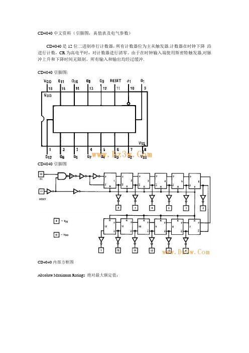
CD4040中文资料(引脚图,真值表及电气参数)
CD4040是12位二进制串行计数器,所有计数器位为主从触发器.计数器在时钟下降沿进行计数,CR为高电平时,对计数器进行清零。
由于在时钟输入端使用斯密特触发器,对脉冲上升和下降时间无限制。
所有输入和输出均经过缓冲.
CD4040引脚图:
CD4040引脚图
CD4040内部方框图
Absolute Maximum Ratings 绝对最大额定值:
CD4040应用电路:
秒基准脉冲产生电路图
IC1(CD4060)的32768 Hz的振荡源经14级分频后在输出端3脚(Q14)得到1/2S脉冲并冲入由IC2(CD4040)构成的二分频器,分频后在输出端IC2的9脚上得到秒基准脉冲.。
- 1、下载文档前请自行甄别文档内容的完整性,平台不提供额外的编辑、内容补充、找答案等附加服务。
- 2、"仅部分预览"的文档,不可在线预览部分如存在完整性等问题,可反馈申请退款(可完整预览的文档不适用该条件!)。
- 3、如文档侵犯您的权益,请联系客服反馈,我们会尽快为您处理(人工客服工作时间:9:00-18:30)。
Data sheet acquired from Harris Semiconductor SCHS030D − Revised December 2003The CD4020B and CD4040B types are supplied in 16-lead hermetic dual-in-line ceramic packages (F3A suffix), 16-lead dual-in-line plastic packages (E suffix), 16-lead small-outline packages (NSR suffix), and 16-lead thin shrink small-outline packages (PW and PWR suffixes). The CD4040B type also is supplied in 16-lead small-outline packages (M and M96 suffixes).The CD4024B types are supplied in 14-lead hermetic dual-in-line ceramic packages (F3A suffix), 14-lead dual-in-line plastic packages (E suffix), 14-lead small-outline packages (M, MT, M96, and NSR suffixes), and 14-lead thin shrink small-outline packages (PW and PWR suffixes).IMPORTANT NOTICETexas Instruments Incorporated and its subsidiaries(TI)reserve the right to make corrections,modifications,enhancements, improvements,and other changes to its products and services at any time and to discontinue any product or service without notice. Customers should obtain the latest relevant information before placing orders and should verify that such information is current and complete.All products are sold subject to TI’s terms and conditions of sale supplied at the time of order acknowledgment.TI warrants performance of its hardware products to the specifications applicable at the time of sale in accordance with TI’s standard warranty.Testing and other quality control techniques are used to the extent TI deems necessary to support this warranty.Except where mandated by government requirements,testing of all parameters of each product is not necessarily performed.TI assumes no liability for applications assistance or customer product design.Customers are responsible for their products and applications using TI components.To minimize the risks associated with customer products and applications,customers should provide adequate design and operating safeguards.TI does not warrant or represent that any license,either express or implied,is granted under any TI patent right,copyright,mask work right,or other TI intellectual property right relating to any combination,machine,or process in which TI products or services are rmation published by TI regarding third-party products or services does not constitute a license from TI to use such products or services or a warranty or endorsement e of such information may require a license from a third party under the patents or other intellectual property of the third party,or a license from TI under the patents or other intellectual property of TI. Reproduction of information in TI data books or data sheets is permissible only if reproduction is without alteration and is accompanied by all associated warranties,conditions,limitations,and notices.Reproduction of this information with alteration is an unfair and deceptive business practice.TI is not responsible or liable for such altered documentation.Resale of TI products or services with statements different from or beyond the parameters stated by TI for that product or service voids all express and any implied warranties for the associated TI product or service and is an unfair and deceptive business practice.TI is not responsible or liable for any such statements.TI products are not authorized for use in safety-critical applications(such as life support)where a failure of the TI product would reasonably be expected to cause severe personal injury or death,unless officers of the parties have executed an agreement specifically governing such use.Buyers represent that they have all necessary expertise in the safety and regulatory ramifications of their applications,and acknowledge and agree that they are solely responsible for all legal,regulatory and safety-related requirements concerning their products and any use of TI products in such safety-critical applications,notwithstanding any applications-related information or support that may be provided by TI.Further,Buyers must fully indemnify TI and its representatives against any damages arising out of the use of TI products in such safety-critical applications.TI products are neither designed nor intended for use in military/aerospace applications or environments unless the TI products are specifically designated by TI as military-grade or"enhanced plastic."Only products designated by TI as military-grade meet military specifications.Buyers acknowledge and agree that any such use of TI products which TI has not designated as military-grade is solely at the Buyer's risk,and that they are solely responsible for compliance with all legal and regulatory requirements in connection with such use.TI products are neither designed nor intended for use in automotive applications or environments unless the specific TI products are designated by TI as compliant with ISO/TS16949requirements.Buyers acknowledge and agree that,if they use anynon-designated products in automotive applications,TI will not be responsible for any failure to meet such requirements. Following are URLs where you can obtain information on other Texas Instruments products and application solutions:Products ApplicationsAmplifiers AudioData Converters AutomotiveDSP BroadbandInterface Digital ControlLogic MilitaryPower Mgmt Optical NetworkingMicrocontrollers SecurityLow Power TelephonyWirelessVideo&ImagingWirelessMailing Address:Texas Instruments,Post Office Box655303,Dallas,Texas75265Copyright©2007,Texas Instruments IncorporatedPACKAGING INFORMATIONOrderable Device Status(1)PackageType PackageDrawingPins PackageQtyEco Plan(2)Lead/Ball Finish MSL Peak Temp(3)89271AKB3T OBSOLETE CFP WR16TBD Call TI Call TI89274AKB3T OBSOLETE CFP WR16TBD Call TI Call TICD4020BE ACTIVE PDIP N1625Pb-Free(RoHS)CU NIPDAU N/A for Pkg TypeCD4020BEE4ACTIVE PDIP N1625Pb-Free(RoHS)CU NIPDAU N/A for Pkg Type CD4020BF ACTIVE CDIP J161TBD A42SNPB N/A for Pkg Type CD4020BF3A ACTIVE CDIP J161TBD A42SNPB N/A for Pkg Type CD4020BNSR ACTIVE SO NS162000Green(RoHS&no Sb/Br)CU NIPDAU Level-1-260C-UNLIMCD4020BNSRE4ACTIVE SO NS162000Green(RoHS&no Sb/Br)CU NIPDAU Level-1-260C-UNLIMCD4020BNSRG4ACTIVE SO NS162000Green(RoHS&no Sb/Br)CU NIPDAU Level-1-260C-UNLIMCD4020BPW ACTIVE TSSOP PW1690Green(RoHS&no Sb/Br)CU NIPDAU Level-1-260C-UNLIMCD4020BPWE4ACTIVE TSSOP PW1690Green(RoHS&no Sb/Br)CU NIPDAU Level-1-260C-UNLIMCD4020BPWG4ACTIVE TSSOP PW1690Green(RoHS&no Sb/Br)CU NIPDAU Level-1-260C-UNLIMCD4020BPWR ACTIVE TSSOP PW162000Green(RoHS&no Sb/Br)CU NIPDAU Level-1-260C-UNLIMCD4020BPWRE4ACTIVE TSSOP PW162000Green(RoHS&no Sb/Br)CU NIPDAU Level-1-260C-UNLIMCD4020BPWRG4ACTIVE TSSOP PW162000Green(RoHS&no Sb/Br)CU NIPDAU Level-1-260C-UNLIMCD4024BE ACTIVE PDIP N1425Pb-Free(RoHS)CU NIPDAU N/A for Pkg TypeCD4024BEE4ACTIVE PDIP N1425Pb-Free(RoHS)CU NIPDAU N/A for Pkg Type CD4024BF ACTIVE CDIP J141TBD A42SNPB N/A for Pkg Type CD4024BF3A ACTIVE CDIP J141TBD A42SNPB N/A for Pkg Type CD4024BF3AS2534OBSOLETE CDIP J14TBD Call TI Call TI CD4024BM ACTIVE SOIC D1450Green(RoHS&no Sb/Br)CU NIPDAU Level-1-260C-UNLIMCD4024BM96ACTIVE SOIC D142500Green(RoHS&no Sb/Br)CU NIPDAU Level-1-260C-UNLIMCD4024BM96E4ACTIVE SOIC D142500Green(RoHS&no Sb/Br)CU NIPDAU Level-1-260C-UNLIMCD4024BM96G4ACTIVE SOIC D142500Green(RoHS&no Sb/Br)CU NIPDAU Level-1-260C-UNLIMCD4024BME4ACTIVE SOIC D1450Green(RoHS&no Sb/Br)CU NIPDAU Level-1-260C-UNLIMCD4024BMG4ACTIVE SOIC D1450Green(RoHS&no Sb/Br)CU NIPDAU Level-1-260C-UNLIMCD4024BMT ACTIVE SOIC D14250Green(RoHS&no Sb/Br)CU NIPDAU Level-1-260C-UNLIM CD4024BMTE4ACTIVE SOIC D14250Green(RoHS&CU NIPDAU Level-1-260C-UNLIMOrderable Device Status(1)PackageType PackageDrawingPins PackageQtyEco Plan(2)Lead/Ball Finish MSL Peak Temp(3)no Sb/Br)CD4024BMTG4ACTIVE SOIC D14250Green(RoHS&no Sb/Br)CU NIPDAU Level-1-260C-UNLIMCD4024BNSR ACTIVE SO NS142000Green(RoHS&no Sb/Br)CU NIPDAU Level-1-260C-UNLIMCD4024BNSRE4ACTIVE SO NS142000Green(RoHS&no Sb/Br)CU NIPDAU Level-1-260C-UNLIMCD4024BNSRG4ACTIVE SO NS142000Green(RoHS&no Sb/Br)CU NIPDAU Level-1-260C-UNLIMCD4024BPW ACTIVE TSSOP PW1490Green(RoHS&no Sb/Br)CU NIPDAU Level-1-260C-UNLIMCD4024BPWE4ACTIVE TSSOP PW1490Green(RoHS&no Sb/Br)CU NIPDAU Level-1-260C-UNLIMCD4024BPWG4ACTIVE TSSOP PW1490Green(RoHS&no Sb/Br)CU NIPDAU Level-1-260C-UNLIMCD4024BPWR ACTIVE TSSOP PW142000Green(RoHS&no Sb/Br)CU NIPDAU Level-1-260C-UNLIMCD4024BPWRE4ACTIVE TSSOP PW142000Green(RoHS&no Sb/Br)CU NIPDAU Level-1-260C-UNLIMCD4024BPWRG4ACTIVE TSSOP PW142000Green(RoHS&no Sb/Br)CU NIPDAU Level-1-260C-UNLIMCD4040BE ACTIVE PDIP N1625Pb-Free(RoHS)CU NIPDAU N/A for Pkg TypeCD4040BEE4ACTIVE PDIP N1625Pb-Free(RoHS)CU NIPDAU N/A for Pkg Type CD4040BF ACTIVE CDIP J161TBD A42SNPB N/A for Pkg Type CD4040BF3A ACTIVE CDIP J161TBD A42SNPB N/A for Pkg Type CD4040BM ACTIVE SOIC D1640Green(RoHS&no Sb/Br)CU NIPDAU Level-1-260C-UNLIMCD4040BM96ACTIVE SOIC D162500Green(RoHS&no Sb/Br)CU NIPDAU Level-1-260C-UNLIMCD4040BM96E4ACTIVE SOIC D162500Green(RoHS&no Sb/Br)CU NIPDAU Level-1-260C-UNLIMCD4040BM96G4ACTIVE SOIC D162500Green(RoHS&no Sb/Br)CU NIPDAU Level-1-260C-UNLIMCD4040BME4ACTIVE SOIC D1640Green(RoHS&no Sb/Br)CU NIPDAU Level-1-260C-UNLIMCD4040BMG4ACTIVE SOIC D1640Green(RoHS&no Sb/Br)CU NIPDAU Level-1-260C-UNLIMCD4040BNSR ACTIVE SO NS162000Green(RoHS&no Sb/Br)CU NIPDAU Level-1-260C-UNLIMCD4040BNSRE4ACTIVE SO NS162000Green(RoHS&no Sb/Br)CU NIPDAU Level-1-260C-UNLIMCD4040BNSRG4ACTIVE SO NS162000Green(RoHS&no Sb/Br)CU NIPDAU Level-1-260C-UNLIMCD4040BPW ACTIVE TSSOP PW1690Green(RoHS&no Sb/Br)CU NIPDAU Level-1-260C-UNLIMCD4040BPWE4ACTIVE TSSOP PW1690Green(RoHS&no Sb/Br)CU NIPDAU Level-1-260C-UNLIMCD4040BPWG4ACTIVE TSSOP PW1690Green(RoHS&no Sb/Br)CU NIPDAU Level-1-260C-UNLIMOrderable Device Status(1)PackageType PackageDrawingPins PackageQtyEco Plan(2)Lead/Ball Finish MSL Peak Temp(3)CD4040BPWR ACTIVE TSSOP PW162000Green(RoHS&no Sb/Br)CU NIPDAU Level-1-260C-UNLIMCD4040BPWRE4ACTIVE TSSOP PW162000Green(RoHS&no Sb/Br)CU NIPDAU Level-1-260C-UNLIMCD4040BPWRG4ACTIVE TSSOP PW162000Green(RoHS&no Sb/Br)CU NIPDAU Level-1-260C-UNLIM JM38510/05653BEA ACTIVE CDIP J161TBD A42SNPB N/A for Pkg Type JM38510/05655BCA ACTIVE CDIP J141TBD A42SNPB N/A for Pkg Type (1)The marketing status values are defined as follows:ACTIVE:Product device recommended for new designs.LIFEBUY:TI has announced that the device will be discontinued,and a lifetime-buy period is in effect.NRND:Not recommended for new designs.Device is in production to support existing customers,but TI does not recommend using this part in a new design.PREVIEW:Device has been announced but is not in production.Samples may or may not be available.OBSOLETE:TI has discontinued the production of the device.(2)Eco Plan-The planned eco-friendly classification:Pb-Free(RoHS),Pb-Free(RoHS Exempt),or Green(RoHS&no Sb/Br)-please check /productcontent for the latest availability information and additional product content details.TBD:The Pb-Free/Green conversion plan has not been defined.Pb-Free(RoHS):TI's terms"Lead-Free"or"Pb-Free"mean semiconductor products that are compatible with the current RoHS requirements for all6substances,including the requirement that lead not exceed0.1%by weight in homogeneous materials.Where designed to be soldered at high temperatures,TI Pb-Free products are suitable for use in specified lead-free processes.Pb-Free(RoHS Exempt):This component has a RoHS exemption for either1)lead-based flip-chip solder bumps used between the die and package,or2)lead-based die adhesive used between the die and leadframe.The component is otherwise considered Pb-Free(RoHS compatible)as defined above.Green(RoHS&no Sb/Br):TI defines"Green"to mean Pb-Free(RoHS compatible),and free of Bromine(Br)and Antimony(Sb)based flame retardants(Br or Sb do not exceed0.1%by weight in homogeneous material)(3)MSL,Peak Temp.--The Moisture Sensitivity Level rating according to the JEDEC industry standard classifications,and peak solder temperature.Important Information and Disclaimer:The information provided on this page represents TI's knowledge and belief as of the date that it is provided.TI bases its knowledge and belief on information provided by third parties,and makes no representation or warranty as to the accuracy of such information.Efforts are underway to better integrate information from third parties.TI has taken and continues to take reasonable steps to provide representative and accurate information but may not have conducted destructive testing or chemical analysis on incoming materials and chemicals.TI and TI suppliers consider certain information to be proprietary,and thus CAS numbers and other limited information may not be available for release.In no event shall TI's liability arising out of such information exceed the total purchase price of the TI part(s)at issue in this document sold by TI to Customer on an annual basis.TAPE AND REEL INFORMATION*All dimensions are nominalDevicePackage Type Package Drawing Pins SPQReel Diameter (mm)Reel Width W1(mm)A0(mm)B0(mm)K0(mm)P1(mm)W (mm)Pin1Quadrant CD4020BNSR SO NS 162000330.016.48.210.5 2.512.016.0Q1CD4020BPWR TSSOP PW 162000330.012.47.0 5.6 1.68.012.0Q1CD4024BM96SOIC D 142500330.016.4 6.59.0 2.18.016.0Q1CD4024BNSR SO NS 142000330.016.48.210.5 2.512.016.0Q1CD4024BPWR TSSOP PW 142000330.012.47.0 5.6 1.68.012.0Q1CD4040BM96SOIC D 162500330.016.4 6.510.3 2.18.016.0Q1CD4040BNSR SO NS 162000330.016.48.210.5 2.512.016.0Q1CD4040BPWRTSSOPPW162000330.012.47.05.61.68.012.0Q1*All dimensions are nominalDevice Package Type Package Drawing Pins SPQ Length(mm)Width(mm)Height(mm) CD4020BNSR SO NS162000346.0346.033.0 CD4020BPWR TSSOP PW162000346.0346.029.0 CD4024BM96SOIC D142500346.0346.033.0 CD4024BNSR SO NS142000346.0346.033.0 CD4024BPWR TSSOP PW142000346.0346.029.0 CD4040BM96SOIC D162500333.2345.928.6 CD4040BNSR SO NS162000346.0346.033.0 CD4040BPWR TSSOP PW162000346.0346.029.0。