UC2863中文资料
UC3853中文资料

PACKAGING INFORMATIONOrderable Device Status (1)Package Type Package Drawing Pins Package Qty Eco Plan (2)Lead/Ball Finish MSL Peak Temp (3)UCC28521DW ACTIVE SOIC DW 2025TBD CU NIPDAU Level-1-220C-UNLIM UCC28521DWR ACTIVE SOIC DW 202000TBD CU NIPDAU Level-1-220C-UNLIM UCC28528DW ACTIVE SOIC DW 2025TBD CU NIPDAU Level-1-220C-UNLIM UCC28528DWRACTIVESOICDW202000TBDCU NIPDAULevel-1-220C-UNLIM(1)The marketing status values are defined as follows:ACTIVE:Product device recommended for new designs.LIFEBUY:TI has announced that the device will be discontinued,and a lifetime-buy period is in effect.NRND:Not recommended for new designs.Device is in production to support existing customers,but TI does not recommend using this part in a new design.PREVIEW:Device has been announced but is not in production.Samples may or may not be available.OBSOLETE:TI has discontinued the production of the device.(2)Eco Plan -The planned eco-friendly classification:Pb-Free (RoHS)or Green (RoHS &no Sb/Br)-please check /productcontent for the latest availability information and additional product content details.TBD:The Pb-Free/Green conversion plan has not been defined.Pb-Free (RoHS):TI's terms "Lead-Free"or "Pb-Free"mean semiconductor products that are compatible with the current RoHS requirements for all 6substances,including the requirement that lead not exceed 0.1%by weight in homogeneous materials.Where designed to be soldered at high temperatures,TI Pb-Free products are suitable for use in specified lead-free processes.Green (RoHS &no Sb/Br):TI defines "Green"to mean Pb-Free (RoHS compatible),and free of Bromine (Br)and Antimony (Sb)based flame retardants (Br or Sb do not exceed 0.1%by weight in homogeneous material)(3)MSL,Peak Temp.--The Moisture Sensitivity Level rating according to the JEDEC industry standard classifications,and peak solder temperature.Important Information and Disclaimer:The information provided on this page represents TI's knowledge and belief as of the date that it is provided.TI bases its knowledge and belief on information provided by third parties,and makes no representation or warranty as to theaccuracy of such information.Efforts are underway to better integrate information from third parties.TI has taken and continues to take reasonable steps to provide representative and accurate information but may not have conducted destructive testing or chemical analysis on incoming materials and chemicals.TI and TI suppliers consider certain information to be proprietary,and thus CAS numbers and other limited information may not be available for release.In no event shall TI's liability arising out of such information exceed the total purchase price of the TI part(s)at issue in this document sold by TI to Customer on an annual basis.PACKAGE OPTION ADDENDUM27-Jun-2005Addendum-Page 1元器件交易网IMPORTANT NOTICETexas Instruments Incorporated and its subsidiaries (TI) reserve the right to make corrections, modifications, enhancements, improvements, and other changes to its products and services at any time and to discontinue any product or service without notice. Customers should obtain the latest relevant information before placing orders and should verify that such information is current and complete. All products are sold subject to TI’s terms and conditions of sale supplied at the time of order acknowledgment.TI warrants performance of its hardware products to the specifications applicable at the time of sale in accordance with TI’s standard warranty. T esting and other quality control techniques are used to the extent TI deems necessary to support this warranty. Except where mandated by government requirements, testing of all parameters of each product is not necessarily performed.TI assumes no liability for applications assistance or customer product design. Customers are responsible for their products and applications using TI components. T o minimize the risks associated with customer products and applications, customers should provide adequate design and operating safeguards.TI does not warrant or represent that any license, either express or implied, is granted under any TI patent right, copyright, mask work right, or other TI intellectual property right relating to any combination, machine, or process in which TI products or services are used. Information published by TI regarding third-party products or services does not constitute a license from TI to use such products or services or a warranty or endorsement thereof. Use of such information may require a license from a third party under the patents or other intellectual property of the third party, or a license from TI under the patents or other intellectual property of TI.Reproduction of information in TI data books or data sheets is permissible only if reproduction is without alteration and is accompanied by all associated warranties, conditions, limitations, and notices. Reproduction of this information with alteration is an unfair and deceptive business practice. TI is not responsible or liable for such altered documentation.Resale of TI products or services with statements different from or beyond the parameters stated by TI for that product or service voids all express and any implied warranties for the associated TI product or service and is an unfair and deceptive business practice. TI is not responsible or liable for any such statements. Following are URLs where you can obtain information on other Texas Instruments products and application solutions:Products ApplicationsAmplifiers Audio /audioData Converters Automotive /automotiveDSP Broadband /broadbandInterface Digital Control /digitalcontrolLogic Military /militaryPower Mgmt Optical Networking /opticalnetwork Microcontrollers Security /securityTelephony /telephonyVideo & Imaging /videoWireless /wirelessMailing Address:Texas InstrumentsPost Office Box 655303 Dallas, Texas 75265Copyright 2005, Texas Instruments Incorporated。
ET80960JA3V252中文资料

80960JA/JF/JD/JS/JC/JT 3.3 V Embedded 32-Bit MicroprocessorDatasheetProduct Featuress Code Compatible with all 80960Jx ProcessorssHigh-Performance Embedded Architecture —One Instruction/Clock Execution —Core Clock Rate is:1x the Bus Clock for 80960JA/JF/JS 2x the Bus Clock for 80960JD/JC 3x the Bus Clock for 80960JT —Load/Store Programming Model —Sixteen 32-Bit Global Registers—Sixteen 32-Bit Local Registers (8 sets)—Nine Addressing Modes—User/Supervisor Protection Model sTwo-Way Set Associative Instruction Cache—80960JA - 2Kbyte —80960JF/JD - 4Kbyte —80960JS/JC/JT - 16Kbyte —Programmable Cache-Locking MechanismsDirect Mapped Data Cache —80960JA - 1Kbyte —80960JF/JD - 2Kbyte —80960JS/JC/JT - 4Kbyte —Write Through Operation sOn-Chip Stack Frame Cache—Seven Register Sets May Be Saved —Automatic Allocation on Call/Return —0-7 Frames Reserved for High-Priority InterruptssOn-Chip Data RAM—1Kbyte Critical Variable Storage —Single-Cycle Access s3.3V Supply Voltage —5V Tolerant Inputs—TTL Compatible Outputs sHigh Bandwidth Burst Bus—32-Bit Multiplexed Address/Data—Programmable Memory Configuration —Selectable 8-, 16-, 32-Bit Bus Widths —Supports Unaligned Accesses—Big or Little Endian Byte Ordering sHigh-Speed Interrupt Controller —31 Programmable Priorities —Eight Maskable Pins plus NMI#—Up to 240 Vectors in Expanded Mode sTwo On-Chip Timers—Independent 32-Bit Counting —Clock Prescaling by 1, 2, 4 or 8—Internal Interrupt Sources s Halt Mode for Low Powers IEEE 1149.1 (JTAG) Boundary Scan Compatibility sPackages—132-Lead Pin Grid Array (PGA)—132-Lead Plastic Quad Flat Pack (PQFP)—196-Ball Mini Plastic Ball Grid Array (MPBGA)Order Number: 273159-006August 2004INFORMATION IN THIS DOCUMENT IS PROVIDED IN CONNECTION WITH INTEL® PRODUCTS. NO LICENSE, EXPRESS OR IMPLIED, BY ESTOPPEL OR OTHERWISE, TO ANY INTELLECTUAL PROPERTY RIGHTS IS GRANTED BY THIS DOCUMENT. EXCEPT AS PROVIDED IN INTEL’S TERMS AND CONDITIONS OF SALE FOR SUCH PRODUCTS, INTEL ASSUMES NO LIABILITY WHATSOEVER, AND INTEL DISCLAIMS ANY EXPRESS OR IMPLIED WARRANTY, RELATING TO SALE AND/OR USE OF INTEL PRODUCTS INCLUDING LIABILITY OR WARRANTIES RELATING TO FITNESS FOR A PARTICULAR PURPOSE, MERCHANTABILITY, OR INFRINGEMENT OF ANY PATENT, COPYRIGHT OR OTHER INTELLECTUAL PROPERTY RIGHT. Intel products are not intended for use in medical, life saving, life sustaining applications.Intel may make changes to specifications and product descriptions at any time, without notice.Designers must not rely on the absence or characteristics of any features or instructions marked "reserved" or "undefined." Intel reserves these for future definition and shall have no responsibility whatsoever for conflicts or incompatibilities arising from future changes to them.The 80960JA/JF/JD/JS/JC/JT 3.3 V Embedded 32-Bit Microprocessor may contain design defects or errors known as errata which may cause the product to deviate from published specifications. Current characterized errata are available on request.Contact your local Intel sales office or your distributor to obtain the latest specifications and before placing your product order.Copies of documents which have an ordering number and are referenced in this document, or other Intel literature may be obtained by calling1-800-548-4725 or by visiting Intel’s website at .AlertVIEW, AnyPoint, AppChoice, BoardWatch, BunnyPeople, CablePort, Celeron, Chips, CT Connect, CT Media, Dialogic, DM3, EtherExpress, ETOX, FlashFile, i386, i486, i960, iCOMP, InstantIP, Intel, Intel logo, Intel386, Intel486, Intel740, IntelDX2, IntelDX4, IntelSX2, Intel Create & Share, Intel GigaBlade, Intel InBusiness, Intel Inside, Intel Inside logo, Intel NetBurst, Intel NetMerge, Intel NetStructure, Intel Play, Intel Play logo, Intel SingleDriver, Intel SpeedStep, Intel StrataFlash, Intel TeamStation, Intel Xeon, Intel XScale, IPLink, Itanium, LANDesk, LanRover, MCS, MMX, MMX logo, Optimizer logo, OverDrive, Paragon, PC Dads, PC Parents, PDCharm, Pentium, Pentium II Xeon, Pentium III Xeon, Performance at Your Command, RemoteExpress, Shiva, SmartDie, Solutions960, Sound Mark, StorageExpress, The Computer Inside., The Journey Inside, TokenExpress, Trillium, VoiceBrick, Vtune, and Xircom are trademarks or registered trademarks of Intel Corporation or its subsidiaries in the United States and other countries.*Other names and brands may be claimed as the property of others.Copyright © Intel Corporation, 2002, 2004Contents Contents1.0Introduction (7)2.080960Jx Overview (9)2.180960 Processor Core (10)2.2Burst Bus (11)2.3Timer Unit (11)2.4Priority Interrupt Controller (11)2.5Instruction Set Summary (12)2.6Faults and Debugging (12)2.7Low Power Operation (12)2.8Test Features (12)2.9Memory-Mapped Control Registers (13)2.10Data Types and Memory Addressing Modes (13)3.0Packaging Information (15)3.1Available Processors and Packages (15)3.2Pin Descriptions (16)3.2.1Functional Pin Definitions (16)3.2.280960Jx 132-Lead PGA Pinout (23)3.2.380960Jx 132-Lead PQFP Pinout (27)3.2.480960Jx 196-Ball MPBGA Pinout (30)4.0Electrical Specifications (35)4.1Absolute Maximum Ratings (35)4.2Operating Conditions (35)4.3Connection Recommendations (36)4.4VCC5 Pin Requirements (VDIFF) (36)4.5VCCPLL Pin Requirements (37)4.6 D.C. Specifications (38)4.7 A.C. Specifications (42)4.7.1 A.C. Test Conditions and Derating Curves (45)4.7.1.1Output Delay or Hold vs. Load Capacitance (46)4.7.1.2T LX vs. AD Bus Load Capacitance (47)4.7.1.3ICC Active vs. Frequency (49)4.7.2 A.C. Timing Waveforms (53)5.0Device Identification (59)5.180960JS/JC/JT Device Identification Register (60)5.280960JD Device Identification Register (61)5.380960JA/JF Device Identification Register (62)6.0Thermal Specifications (63)6.1Thermal Management Accessories (68)6.1.1Heatsinks (68)7.0Bus Functional Waveforms (69)7.1Basic Bus States (79)7.2Boundary-Scan Register (80)ContentsFigures180960Jx Microprocessor Package Options (7)280960Jx Block Diagram (10)3132-Lead Pin Grid Array Top View-Pins Facing Down (23)4132-Lead Pin Grid Array Bottom View-Pins Facing Up (24)5132-Lead PQFP - Top View (27)6196-Ball Mini Plastic Ball Grid Array Top View-Balls Facing Down (30)7196-Ball Mini Plastic Ball Grid Array Bottom View-Balls Facing Up (31)8VCC5 Current-Limiting Resistor (36)9VCCPLL Lowpass Filter (37)10 A.C. Test Load (45)11Output Delay or Hold vs. Load Capacitance–80960JS/JC/JT (3.3 V Signals) (46)12Output Delay or Hold vs. Load Capacitance–80960JS/JC/JT (5V Signals) (46)13Output Delay or Hold vs. Load Capacitance–80960JA/JF/JD (47)14T LX vs. AD Bus Load Capacitance–80960JS/JC/JT (3.3V Signals) (47)15T LX vs. AD Bus Load Capacitance–80960JS/JC/JT (5V Signals) (48)16T LX vs. AD Bus Load Capacitance–80960JA/JF/JD (48)17I CC Active (Power Supply) vs. Frequency–80960JA/JF (49)1880960JA/JF I CC Active (Thermal) vs. Frequency (49)1980960JD I CC Active (Power Supply) vs. Frequency (50)2080960JD I CC Active (Thermal) vs. Frequency (50)2180960JC I CC Active (Power Supply) vs. Frequency (51)2280960JC I CC Active (Thermal) vs. Frequency (51)2380960JS I CC Active (Power Supply) vs. Frequency (52)2480960JS I CC Active (Thermal) vs. Frequency (52)25CLKIN Waveform (53)26T OV1 Output Delay Waveform (53)27T OF Output Float Waveform (54)28T IS1 and T IH1 Input Setup and Hold Waveform (54)29T IS2 and T IH2 Input Setup and Hold Waveform (54)30T IS3 and T IH3 Input Setup and Hold Waveform (55)31T IS4 and T IH4 Input Setup and Hold Waveform (55)32T LX, T LXL and T LXA Relative Timings Waveform (56)33DT/R# and DEN# Timings Waveform (56)34TCK Waveform (57)35T BSIS1 and T BSIH1 Input Setup and Hold Waveforms (57)36T BSOV1 and T BSOF1 Output Delay and Output Float Waveform (57)37T BSOV2 and T BSOF2 Output Delay and Output Float Waveform (58)38T BSIS2 and T BSIH2 Input Setup and Hold Waveform (58)3980960JS/JC/JT Device Identification Register Fields (60)4080960JD Device Identification Register Fields (61)4180960JA/JF Device Identification Register Fields (62)42Non-Burst Read and Write Transactions Without Wait States, 32-Bit Bus (69)43Burst Read and Write Transactions Without Wait States, 32-Bit Bus (70)44Burst Write Transactions With 2,1,1,1 Wait States, 32-Bit Bus (71)45Burst Read and Write Transactions Without Wait States, 8-Bit Bus (72)46Burst Read and Write Transactions With 1, 0 Wait Statesand Extra Tr State on Read, 16-Bit Bus (73)47Double Word Read Bus Request, Misaligned One Byte FromQuad Word Boundary, 32-Bit Bus, Little Endian (74)Contents 48HOLD/HOLDA Waveform For Bus Arbitration (75)49Cold Reset Waveform (76)50Warm Reset Waveform (77)51Entering the ONCE State (78)52Bus States with Arbitration (80)53Summary of Aligned and Unaligned Accesses (32-Bit Bus) (84)54Summary of Aligned and Unaligned Accesses (32-Bit Bus) (Continued) (85)Tables180960Jx 3.3-V Microprocessor Family (7)280960Jx Instruction Set (14)380960Jx Processors Available in 132-Pin PGA Package (15)480960Jx Processors Available in 132-Pin PQFP Package (15)580960Jx Processors Available in Extended Temperature (16)680960Jx Processors Available in 196-Ball MPBGA Package (16)7Pin Description Nomenclature (17)8Pin Description—External Bus Signals (18)9Pin Description—Processor Control Signals, Test Signals, and Power (21)10Pin Description—Interrupt Unit Signals (22)11132-Lead PGA Pinout—In Signal Order (25)12132-Lead PGA Pinout—In Pin Order (26)13132-Lead PQFP Pinout—In Signal Order (28)14132-Lead PQFP Pinout—In Pin Order (29)15196-Ball MPBGA Pinout—In Signal Order (32)16196-Ball MPBGA Pinout—In Pin Order (33)17Absolute Maximum Ratings (35)1880960Jx Operating Conditions (35)19VDIFF Parameters (37)2080960Jx D.C. Characteristics (38)2180960Jx I CC Characteristics (39)2280960Jx A.C. Characteristics (42)23Note Definitions for Table 22, 80960Jx AC Characteristics (45)2480960Jx Device Type and Stepping Reference (59)2580960JS/JC/JT Device ID Register Field Definitions (60)2680960JS/JC/JT Device ID Model Types (60)2780960JD Device ID Field Definitions (61)2880960JD Device ID Model Types (61)2980960JA/JF Device ID Field Definitions (62)3080960JA/JF Device ID Model Types (62)31Thermal Resistance for q CA and q JC Reference Table (63)32Maximum Ambient Temperature Reference Table (63)33132-Lead PGA Package Thermal Characteristics (64)3480960JA/JF/JD 196-Ball MPBGA Package Thermal Characteristics (64)3580960JS/JC/JT 196-Ball MPBGA Package Thermal Characteristics (65)36132-Lead PQFP Package Thermal Characteristics (65)37Maximum T A at Various Airflows in °C (80960JT) (66)38Maximum T A at Various Airflows in °C (80960JC) (66)39Maximum T A at Various Airflows in °C (80960JD) (67)40Maximum T A at Various Airflows in °C (80960JS) (67)41Maximum T A at Various Airflows in °C (80960JA/JF) (68)Contents42Boundary-Scan Register—Bit Order (81)43Natural Boundaries for Load and Store Accesses (81)44Summary of Byte Load and Store Accesses (82)45Summary of Short Word Load and Store Accesses (82)46Summary of n-Word Load and Store Accesses (n = 1, 2, 3, 4) (83)Revision HistoryDate Revision DescriptionSeptember 2002005Removed reference to A80960JF-16 from Table 3 on page15. Removed reference to NG80960JC-40, NG80960JC-33, NG80960JS-16,and NG80960JF-16 from Table 4 on page15.Removed reference to GD80960JC-40, GD80960JC-33, and 80960JS-16 in Table 6 on page16.Removed reference to 80960JC-40, 80960JC-33, 80960JS-16, and 80960JF-16 in Table 18 on page35.Removed reference to 80960JC-40, 80960JC-33, 80960JS-16, and 80960JF-16 from Table 21 on page39.Removed reference to 80960JC-40, 80960JC-33, 80960JS-16 and 80960JF-16 from Table 22 on page42.September 1999004Added new extended temp device offerings. See Table 5 on page16. Removed PGA package availability from JS/JC/JT processors. Changed AC timing parameter T OV1 (min) for extended temp devices only.See Table 22 on page42.June 1999003Merged the 80960JS/JC datasheet information into this datasheet (previously named 80960JA/JF/JD/JT 3.3V Embedded 32-Bit Microprocessor datasheet).Updated I CC values for the 80960JS/JC/JT processors. Increased TIH1 specification for the 80960JS/JC/JT processors. Updated MPBGA thermal specifications.December 1998002Corrected orientation of MPBGA package diagrams (Figure 6 on page30 and Figure 7 on page31).Added Figure 11 on page46,Figure 12 on page46,Figure 14 on page47, and Figure 15 on page48 to distinguish 80960JT 3.3-V and 5-V signal derating curves from the 80960JA/JF/JD derating curves.March 1998001This datasheet supersedes revisions to the following 80960Jx datasheets: #273109 (JT), #272971-002 (JD), and #276146-001 (JA/JF). In addition to combining the documents into one, the following content was changed: Figure 1 on page7: Added MPBGA package to diagram.Section 3.2.4, “80960Jx 196-Ball MPBGA Pinout” on page30: Added new Figures 6 and 7, Tables 10, 11 and 13.Figure 16 on page48: Added with the note that follows the figure.August 2004006To address the fact that many of the package prefix variables have changed, all package prefix variables in this document are now indicated with an "x".80960JA/JF/JD/JS/JC/JT 3.3 V Embedded 32-Bit Microprocessor1.0IntroductionThis document contains information for the 80960Jx microprocessors, including electrical characteristics and package pinout information. Detailed functional descriptions, other than parametric performance, are published in the i960® Jx Microprocessor Developer’s Manual(272483) and may be viewed online at /design/i960/Techinfo/80960JX/.Throughout this datasheet, references to ‘80960Jx’ indicate features that apply to the 3.3-V Jx processors only:Figure 1. 80960Jx Microprocessor Package Optionsi960®iM©19xxx80960JXXXXXXXXX SS132-Pin PQFPTable 1. 80960Jx 3.3-V Microprocessor FamilyProcessor Voltage Instruction Cache Data Cache Core Clock80960JA 3.3 V (5 V Tolerant) 2 Kbyte 1 Kbyte 1x 80960JF 3.3 V (5 V Tolerant) 4 Kbyte 2 Kbyte 1x 80960JD 3.3 V (5 V Tolerant) 4 Kbyte 2 Kbyte 2x 80960JS 3.3 V (5 V Tolerant)16 Kbyte 4 Kbyte 1x 80960JC 3.3 V (5 V Tolerant)16 Kbyte 4 Kbyte 2x 80960JT3.3 V (5 V Tolerant)16 Kbyte4 Kbyte3xNOTE: To address the fact that many of the package prefix variables have changed, all package prefix variables in this document are now indicated with an "x".This page intentionally left blank.80960JA/JF/JD/JS/JC/JT 3.3 V Embedded 32-Bit Microprocessor 2.080960Jx OverviewThe 80960Jx processor offers high performance to cost-sensitive 32-bit embedded applications.The 80960Jx is object code compatible with the 80960 core architecture and is capable of sustainedexecution at the rate of one instruction per clock. This processor’s features include generousinstruction cache, data cache, and data RAM. It also boasts a fast interrupt mechanism anddual-programmable timer units.The 80960Jx processor’s clock multiplication operates the processor core at two or three times thebus clock rate to improve execution performance without increasing the complexity of boarddesigns.Memory subsystems for cost-sensitive embedded applications often impose substantial wait statepenalties. The 80960Jx integrates considerable storage resources on-chip to decouple CPUexecution from the external bus.The 80960Jx rapidly allocates and de-allocates local register sets during context switches. Theprocessor must flush a register set to the stack only when it saves more than seven sets to its localregister cache.A 32-bit multiplexed burst bus provides a high-speed interface to system memory and I/O. A fullcomplement of control signals simplifies the connection of the 80960Jx to external components.The user programs physical and logical memory attributes through memory-mapped controlregisters (MMRs), an extension not found on the i960® Kx, Sx or Cx processors. Physical andlogical configuration registers enable the processor to operate with all combinations of bus widthand data object alignment. The processor supports a homogeneous byte ordering model.This processor integrates two important peripherals: a timer unit and an interrupt controller. Theseand other hardware resources are programmed through memory-mapped control registers, anextension to the familiar i960 processor architecture.The timer unit (TU) offers two independent 32-bit timers for use as real-time system clocks andgeneral-purpose system timing. These operate in either single-shot or auto-reload mode and maygenerate interrupts.The interrupt controller unit (ICU) provides a flexible, low-latency means for requesting interrupts.The ICU provides full programmability of up to 240 interrupt sources into 31 priority levels. TheICU takes advantage of a cached priority table and optional routine caching to minimize interruptlatency. Clock doubling on the 80960JD/JC processors reduces interrupt latency by 40% comparedto the 80960JA/JF, and clock tripling on the 80960JT reduces interrupt latency by 20% comparedto the 80960JD/JC. Local registers may be dedicated to high-priority interrupts to further reducelatency. Acting independently from the core, the ICU compares the priorities of posted interruptswith the current process priority, off-loading this task from the core. The ICU also supports theintegrated timer interrupts.The 80960Jx features a Halt mode designed to support applications where low power consumptionis critical. The halt instruction shuts down instruction execution, resulting in a power savings of upto 90 percent.The 80960Jx’s testability features, including ONCE (On-Circuit Emulation) mode and BoundaryScan (JTAG), provide a powerful environment for design debug and fault diagnosis.80960JA/JF/JD/JS/JC/JT 3.3 V Embedded 32-Bit MicroprocessorThe Solutions960® program features a wide variety of development tools which support the i960 processor family. Many of these tools are developed by partner companies; some are developed by Intel, such as profile-driven optimizing compilers. For more information on these products, contact your local Intel representative.2.180960 Processor CoreThe 80960Jx family is a scalar implementation of the 80960 core architecture. Intel designed this processor core as a very high performance device that is also cost-effective. Factors that contribute to the core ’s performance include:•Core operates at the bus speed with the 80960JA/JF/JS•Core operates at two or three times the bus speed with the 80960JD/JC and 80960JT,respectively•Single-clock execution of most instructions •Independent Multiply/Divide Unit•Efficient instruction pipeline minimizes pipeline break latency•Register and resource scoreboarding allow overlapped instruction execution •128-bit register bus speeds local register caching •Two-way set associative, integrated instruction cache •Direct-mapped, integrated data cache•1-Kbyte integrated data RAM delivers zero wait state program dataFigure 2. 80960Jx Block DiagramProgrammable Interrupt Controller Control Address/Instruction SequencerPhysical Region Configuration Interrupt Port1K Data RAMMemory Interface Execution Multiply UnitDivide UnitMemory-Mapped Register InterfaceData BusGlobal / Local Register FileSRC2DESTSRC1addressControleffective ConstantsGenerationUnitAddress 32-bit Address 32-bit DataBus Request Queuesand Two 32-BitTimers8-SetLocal Register CacheS R C 1S R C 2D E S TPLL, Clocks,Power MgmtBoundary Scan ControllerTAP 5CLKINS R C 1S R C 2D E S TS R C 1D E S T93232-bit buses address / data21Instruction Cache 80960JA - 2K 80960JF/JD - 4K80960JS/JC/JT - 16KDirect Mapped Data Cache 80960JA - 1K 80960JF/JD - 2K 80960JS/JC/JT -1283 Independent 32-Bit SRC1, SRC2, and DEST BusesBus Control Unit80960JA/JF/JD/JS/JC/JT 3.3 V Embedded 32-Bit Microprocessor2.2Burst BusA 32-bit high-performance Bus Controller Unit (BCU) interfaces the 80960Jx to external memoryand peripherals. The BCU fetches instructions and transfers data at the rate of up to four 32-bitwords per six clock cycles. The external address/data bus is multiplexed.Users may configure the 80960Jx’s bus controller to match an application’s fundamental memoryorganization. Physical bus width is register-programmed for up to eight regions. Byte ordering anddata caching are programmed through a group of logical memory templates and a defaults register.The BCU’s features include:•Multiplexed external bus to minimize pin count•32-, 16-, and 8-bit bus widths to simplify I/O interfaces•External ready control for address-to-data, data-to-data and data-to-next-address wait state types•Support for big or little endian byte ordering to facilitate the porting of existing program code•Unaligned bus accesses performed transparently•Three-deep load/store queue to decouple the bus from the coreUpon reset, the 80960Jx conducts an internal self-test. Then, before executing its first instruction, itperforms an external bus confidence test by performing a checksum on the first words of theinitialization boot record (IBR).2.3Timer UnitThe timer unit (TU) contains two independent 32-bit timers that are capable of counting at severalclock rates and generating interrupts. Each is programmed by use of the TU registers. Thesememory-mapped registers are addressable on 32-bit boundaries. The timers have a single-shotmode and auto-reload capabilities for continuous operation. Each timer has an independentinterrupt request to the 80960Jx’s interrupt controller. The TU may generate a fault whenunauthorized writes from user mode are detected. Clock prescaling is supported.2.4Priority Interrupt ControllerA programmable interrupt controller manages up to 240 external sources through an 8-bit externalinterrupt port. Alternatively, the interrupt inputs may be configured for individual edge- or level-triggered inputs. The interrupt unit (IU) also accepts interrupts from the two on-chip timer channelsand a single Non-Maskable Interrupt (NMI#) pin. Interrupts are serviced according to their prioritylevels relative to the current process priority.Low interrupt latency is critical to many embedded applications. As part of its highly flexibleinterrupt mechanism, the 80960Jx exploits several techniques to minimize latency:•Interrupt vectors and interrupt handler routines may be reserved on-chip.•Register frames for high-priority interrupt handlers may be cached on-chip.•The interrupt stack may be placed in cacheable memory space.•Interrupt microcode executes at two or three times the bus frequency for the 80960JD/JC and 80960JT, respectively.80960JA/JF/JD/JS/JC/JT 3.3 V Embedded 32-Bit Microprocessor2.5Instruction Set SummaryThe 80960Jx adds several new instructions to the i960 processor core architecture. The newinstructions are:•Conditional Move•Conditional Add•Conditional Subtract•Byte Swap•Halt•Cache Control•Interrupt ControlTable 2 identifies the instructions that the 80960Jx supports. Refer to the i960® Jx MicroprocessorDeveloper’s Manual (272483) for a detailed description of each instruction.2.6Faults and DebuggingThe 80960Jx employs a comprehensive fault model. The processor responds to faults by makingimplicit calls to a fault handling routine. Specific information collected for each fault allows thefault handler to diagnose exceptions and recover appropriately.The processor also has built-in debug capabilities. In software, the 80960Jx may be configured todetect as many as seven different trace event types. Alternatively, mark and fmark instructionsmay generate trace events explicitly in the instruction stream. Hardware breakpoint registers arealso available to trap on execution and data addresses.2.7Low Power OperationIntel fabricates the 80960Jx using an advanced sub-micron manufacturing process. The processor’ssub-micron topology provides the circuit density for optimal cache size and high operating speedswhile dissipating modest power. The processor also uses dynamic power management to turn offclocks to unused circuits.Users may program the 80960Jx to enter Halt mode for maximum power savings. In Halt mode,the processor core stops completely while the integrated peripherals continue to function, reducingoverall power requirements up to 90 percent. Processor execution resumes from internally orexternally generated interrupts.2.8Test FeaturesThe 80960Jx incorporates numerous features that enhance the user’s ability to test both theprocessor and the system to which it is attached. These features include ONCE (On-CircuitEmulation) mode and Boundary Scan (JTAG).80960JA/JF/JD/JS/JC/JT 3.3 V Embedded 32-Bit Microprocessor The 80960Jx provides testability features compatible with IEEE Standard Test Access Port andBoundary Scan Architecture (IEEE Std. 1149.1).One of the boundary scan instructions, HIGHZ, forces the processor to float all its output pins(ONCE mode). ONCE mode may also be initiated at reset without using the boundary scanmechanism.ONCE mode is useful for board-level testing. This feature allows a mounted 80960Jx toelectrically “remove” itself from a circuit board. This allows for system-level testing in which aremote tester, such as an in-circuit emulator, may exercise the processor system.The provided test logic does not interfere with component or circuit board behavior and ensuresthat components function correctly, connections between various components are correct, andvarious components interact correctly on the printed circuit board.The JTAG Boundary Scan feature is an attractive alternative to conventional “bed-of-nails” testing.It may examine connections that might otherwise be inaccessible to a test system.2.9Memory-Mapped Control RegistersThe 80960Jx, although compliant with the i960 processor core, has the added advantage ofmemory-mapped, internal control registers not found on the i960 Kx, Sx or Cx processors. Theseregisters give software the interface to easily read and modify internal control registers.Each of these registers is accessed as a memory-mapped, 32-bit register. Access is accomplishedthrough regular memory-format instructions. The processor ensures that these accesses do notgenerate external bus cycles.2.10Data Types and Memory Addressing ModesAs with all i960 processors, the 80960Jx instruction set supports several data types and formats:•Bit•Bit fields•Integer (8-, 16-, 32-, 64-bit)•Ordinal (8-, 16-, 32-, 64-bit unsigned integers)•Triple word (96 bits)•Quad word (128 bits)The 80960Jx provides a full set of addressing modes for C and assembly programming:•Two Absolute modes•Five Register Indirect modes•Index with displacement•IP with displacement。
HSMS-2863中文资料

-40 -30 -20 -10
0
POWER IN (dBm)
Figure 4. +25°C Output Voltage vs. Input Power, HSMS-2850 at Zero Bias, HSMS-2860 at 3 µA Bias.
VOLTAGE OUT (mV)
.1
∆VF (right scale)
元器件交易网
5
Ordering Information
Specify part number followed by option. For example:
H SMS - 285X #X XX
Bulk or Tape and Reel Option Profile: Low = L Part Number Surface Mount Schottky Hewlett-Packard
Data subject to change. Copyright © 1998 Hewlett-Packard Co.
Figure 1. Typical Forward Current vs. Forward Voltage, HSMS-2850 Series.
10000 RL = 100 KΩ
1000
2.45 GHz
100
915 MHz
10
1 0.1
-50
5.8 GHz
DIODES TESTED IN FIXED-TUNED FR4 MICROSTRIP CIRCUITS.
10E-5 5.0 x 10E-8
1.08 5.0 0.65 2 0.5
元器件交易网
4
VOLTAGE OUT (mV)
FORWARD VOLTAGE DIFFERENCE (mV)
UC2838A资料
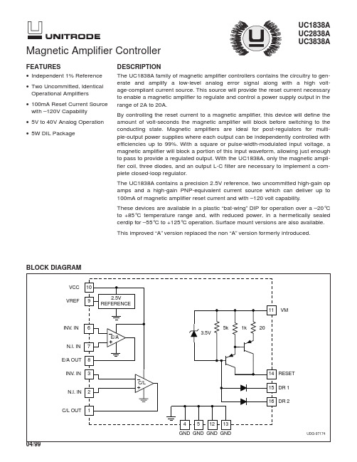
UC2838AUC3838AMagnetic Amplifier ControllerFEATURES•Independent 1% Reference •Two Uncommitted, Identical Operational Amplifiers •100mA Reset Current Source with –120V Capability •5V to 40V Analog Operation •5W DIL Package10VCC VREF92.5V REFERENCEINV .IN 8E/A OUT 3INV .IN67N.I.IN 21N.I.IN C/L OUT C/LE/A3.5V15DR 116DR 2RESET 14VM11512134GND GND GND GND201k 5k BLOCK DIAGRAMUDG-97174DESCRIPTIONThe UC1838A family of magnetic amplifier controllers contains the circuitry to gen-erate and amplify a low-level analog error signal along with a high volt-age-compliant current source.This source will provide the reset current necessary to enable a magnetic amplifier to regulate and control a power supply output in the range of 2A to 20A.By controlling the reset current to a magnetic amplifier,this device will define the amount of volt-seconds the magnetic amplifier will block before switching to the conducting state.Magnetic amplifiers are ideal for post-regulators for multi-ple-output power supplies where each output can be independently controlled with efficiencies up to 99%.With a square or pulse-width-modulated input voltage,a magnetic amplifier will block a portion of this input waveform,allowing just enough to pass to provide a regulated output.With the UC1838A,only the magnetic ampli-fier coil,three diodes,and an output L-C filter are necessary to implement a com-plete closed-loop regulator.The UC1838A contains a precision 2.5V reference,two uncommitted high-gain op amps and a high-gain PNP-equivalent current source which can deliver up to 100mA of magnetic amplifier reset current and with –120 volt capability.These devices are available in a plastic “bat-wing”DIP for operation over a –20°C to +85°C temperature range and,with reduced power,in a hermetically sealed cerdip for –55°C to +125°C operation.Surface mount versions are also available.This improved “A”version replaced the non “A”version formerly introduced.ABSOLUTE MAXIMUM RATINGSSupply Voltage,V CC . . . . . . . . . . . . . . . . . . . . . . . . . . . . . . . . . . . . . . .40V Magnetic Amp. Source Voltage,V M . . . . . . . . . . . . . . . . . . . . . . . .40V Reset Output Voltage,V R . . . . . . . . . . . . . . . . . . . . . . . . . . . . . . .–120V Total Current Source Voltage,V M -V R . . . . . . . . . . . . . . . . . .–140V Amplifier Input Range . . . . . . . . . . . . . . . . . . . . . .–0.3V to V CC Reset Input Current,I DR . . . . . . . . . . . . . . . . . . . . . . . . . . . . . . . .–10mA Power Dissipation at T A = 25°CQ, N, DP Package . . . . . . . . . . . . . . . . . . . . . . . . . . . . . .2W J, L Package. . . . . . . . . . . . . . . . . . . . . . . . . . . . . . . . . . .1W Power Dissipation at T (leads/case) = 25°CQ, N, DP Package . . . . . . . . . . . . . . . . . . . . . . . . . . . . . .5W J, L Package. . . . . . . . . . . . . . . . . . . . . . . . . . . . . . . . . . .2W Operating Temperature Range. . . . . . . . . . . .–55°C to +125°C Storage Temperature Range . . . . . . . . . . . . .–65°C to +150°C Lead Temperature (Soldering, 10 sec). . . . . . . . . . . . . .300°CNote:All voltages are with respect to ground pins.All currents are positive into the specified terminal.Consult Packaging section of Databook for thermal limitations and considerations of package.CONNECTION DIAGRAMSTEMPERATURE RANGEPACKAGE UC1838AJ –55°C to +125°CCeramic Dip UC1838AL CLCCUC2838ADP –20°C to +85°CPower SOIC UC2838AN Plastic Dip UC2838AQ PLCCUC3838ADP 0°C to +70°CPower SOIC UC3838AN Plastic Dip UC3838AQPLCCORDERING INFORMATIONELECTRICAL CHARACTERISTICS:Unless otherwise stated, these specifications apply for T A= –55°C to +125°C for the UC1838A, –20°C to +85°C for the UC2838A, and 0°C to +70°C for the UC3838A,V CC= 20V,V M= 5V, T A=T J.PARAMETER TEST CONDITIONS UC1838A / UC2838A UC3838A UNITS MIN TYP MAX MIN TYP MAXReference SectionSupply Current V CC=V M= 40V4848mA Reference Output T A= 25°C 2.47 2.5 2.53 2.45 2.5 2.55V Line Regulation V CC= 5 to 30V15110mV Load Regulation I O= 0 to –2mA520520mV Short Circuit Current V REF= 0V–30–60–30–60mA Temperature Stability*Over Operating Temp. Range15251025mV Amplifier Section(Each Amplifier)Offset Voltage V CM= 2.5V510mV Input Bias Current V IN= 0V–1–1µA Input Offset Current100100nA Minimum Output Swing0.4180.418V Output Sink Current V O=5V1103011030mA Output Source Current V O= 0V–1–10–20–1–10–20mAA VOL V O= 1 to 11V100120100120dBC MRR V IN= 1 to 11V70807080dBP SRR V CC= 10 to 20V7010070100dB Gain Bandwidth*0.60.80.60.8MHz Reset Drive SectionInput Leakage V DR= 40V1010µA Output Leakage V R= –120V–100–100µA Input Current I R= –50mA–1–2–1–2mA Maximum Reset Current I DR= –3mA–100–120–200–100–120–200mA Transconductance I R= –10 to –50mA.03.042.055.03.042.055A/V * These parameters are guaranteed by design but not 100% tested in production.TYPICAL APPLICATIONAPPLICATION INFORMATIONUNITRODE CORPORA TION7 CONTINENT AL BLVD.•MERRIMACK, NH 03054TEL.(603) 424-2410 • FAX (603) 424-3460IMPORTANT NOTICETexas Instruments and its subsidiaries (TI) reserve the right to make changes to their products or to discontinue any product or service without notice, and advise customers to obtain the latest version of relevant information to verify, before placing orders, that information being relied on is current and complete. All products are sold subject to the terms and conditions of sale supplied at the time of order acknowledgement, including those pertaining to warranty, patent infringement, and limitation of liability.TI warrants performance of its semiconductor products to the specifications applicable at the time of sale in accordance with TI’s standard warranty. Testing and other quality control techniques are utilized to the extent TI deems necessary to support this warranty. Specific testing of all parameters of each device is not necessarily performed, except those mandated by government requirements.CERTAIN APPLICATIONS USING SEMICONDUCTOR PRODUCTS MAY INVOLVE POTENTIAL RISKS OF DEATH, PERSONAL INJURY, OR SEVERE PROPERTY OR ENVIRONMENTAL DAMAGE (“CRITICAL APPLICATIONS”). TI SEMICONDUCTOR PRODUCTS ARE NOT DESIGNED, AUTHORIZED, OR WARRANTED TO BE SUITABLE FOR USE IN LIFE-SUPPORT DEVICES OR SYSTEMS OR OTHER CRITICAL APPLICATIONS. INCLUSION OF TI PRODUCTS IN SUCH APPLICATIONS IS UNDERSTOOD TO BE FULLY AT THE CUSTOMER’S RISK.In order to minimize risks associated with the customer’s applications, adequate design and operating safeguards must be provided by the customer to minimize inherent or procedural hazards.TI assumes no liability for applications assistance or customer product design. TI does not warrant or represent that any license, either express or implied, is granted under any patent right, copyright, mask work right, or other intellectual property right of TI covering or relating to any combination, machine, or process in which such semiconductor products or services might be or are used. TI’s publication of information regarding any third party’s products or services does not constitute TI’s approval, warranty or endorsement thereof.Copyright © 1999, Texas Instruments Incorporated。
UC3823中文资料

UC1823UC2823UC3823High Speed PWM ControllerFEATURES•Compatible with Voltage or Current-Mode Topologies•Practical Operation @ Switching Frequencies to 1.0MHz•50ns Propagation Delay to Output•High Current Totem Pole Output (1.5A peak)•Wide Bandwidth Error Amplifier •Fully Latched Logic with Double Pulse Suppression•Pulse-by-Pulse Current Limiting •Soft Start/Max. Duty Cycle Control •Under-Voltage Lockout with Hysteresis •Low Start Up Current (1.1mA)•Trimmed Bandgap Reference (5.1V ±1%)DESCRIPTIONThe UC1823 family of PWM control ICs is optimized for high fre-quency switched mode power supply applications. Particular care was given to minimizing propagation delays through the compara-tors and logic circuitry while maximizing bandwidth and slew rate of the error amplifier. This controller is designed for use in either current-mode or voltage-mode systems with the capability for input voltage feed-forward.Protection circuitry includes a current limit comparator, a TTL com-patible shutdown port, and a soft start pin which will double as a maximum duty cycle clamp. The logic is fully latched to provide jit-ter free operation and prohibit multiple pulses at the output. An un-der-voltage lockout section with 800mV of hysteresis assures low start up current. During under-voltage lockout, the output is high im-pedance. The current limit reference (pin 11) is a DC input voltage to the current limit comparator. Consult specifications for details.These devices feature a totem pole output designed to source and sink high peak currents from capacitive loads, such as the gate of a power MOSFET . The on state is defined as a high level.BLOCK DIAGRAMABSOLUTE MAXIMUM RATINGSSupply Voltage (Pins 15, 13). . . . . . . . . . . . . . . . . . . . . . . . 30V Output Current, Source or Sink (Pin14)DC. . . . . . . . . . . . . . . . . . . . . . . . . . . . . . . . . . . . . . . . . . 0.5A Pulse (0.5µs). . . . . . . . . . . . . . . . . . . . . . . . . . . . . . . . . . 2.0A Analog Inputs (Pins 1, 2, 7, 8, 9, 11). . . . . . . . . . . -0.3V to +6V Clock Output Current (Pin 4). . . . . . . . . . . . . . . . . . . . . . . -5mA Error Amplifier Output Current (Pin 3). . . . . . . . . . . . . . . . 5mA Soft Start Sink Current (Pin 8). . . . . . . . . . . . . . . . . . . . . 20mAOscillator Charging Current (Pin 5). . . . . . . . . . . . . . . . . . -5mA Power Dissipation at T A = 60 °C . . . . . . . . . . . . . . . . . . . . . 1W Storage Temperature Range . . . . . . . . . . . . . . -65°C to +150°C Lead Temperature (Soldering, 10 seconds). . . . . . . . . . 300°C Note:All voltages are with respect to ground, Pin 10.Currents are positive into the specified terminal.Consult Packaging Section of Databook for thermallimitations and considerations of packages.3/97UC3823CONNECTION DIAGRAMSELECTRICAL CHARACTERISTICS:PARAMETERTEST CONDITIONSUC1823UC2823UC3823UNITSMINTYP MAX MIN TYP MAX Reference Section Output Voltage T J = 25°C, l O = 1mA 5.055.10 5.15 5.005.10 5.20V Line Regulation 10 < V CC < 30V 220220mV Load Regulation 1 < I O < 10mA 520520mV Temperature Stability*T MIN < T A < T MAX 0.20.40.20.4mV/°C Total Output Variation*Line, Load, Temp. 5.005.204.955.25Output Noise Voltage*10Hz < f < 10kHz 5050µV Long Term Stability*T J = 125°C, 1000 hrs.525525mV Short Circuit Current V REF =0V -15-50-100-15-50-100mA Oscillator Section Initial Accuracy*T J =25°C 360400440360400440kHz Voltage Stability*10 < V CC < 30V 0.220.22%Temperature Stability*T MIN <T A < T MAX 55%Total Variation*Line, Temp.340460340460kHz Clock Out High 3.9 4.5 3.94.5V Clock Out Low 2.3 2.9 2.3 2.9V Ramp Peak* 2.6 2.8 3.0 2.6 2.8 3.0V Ramp Valley*0.7 1.0 1.250.7 1.0 1.25V Ramp Valley to Peak*1.61.82.01.61.82.0V * These parameters are guaranteed by design but not 100% tested in production.DIL-16, SOIC-16 (TOP VIEW)J or N, DW PackagePLCC-20, LCC-20 (TOP VIEW)Q, L PackagePACKAGE PIN FUNCTION FUNCTION PINN/C 1Inv.2N.I.3E/A Out 4Clock 5N/C 6R T 7C T 8Ramp 9Soft start 10N/C11I LIM /S.D.12Ground 13I LIM REF 14PWR Gnd 15N/C 16V C 17OUT 18V CC19V REF 5.1V 20Unless otherwise noted, these specifications apply for R T = 3.65k, C T =1nF, V CC = 15V, 0°C < T A < +70°C for the UC3823, -25°C < T A < +85°C for the UC2823, and -55°C < T A < +125°C for the UC1823, T A = T J.PARAMETERTEST CONDITIONSUC1823UC2823UC3823UNITSMINTYPMAX MINTYPMAX Error Amplifier Section Input Offset Voltage 1015mV Input Bias Current 0.630.63µA Input Offset Current 0.110.11µA Open Loop Gain 1 < V O < 4V 60956095dB CMRR 1.5 < V CM < 5.5V 75957595dB PSRR10 < V CC < 30V 8511085110dB Output Sink Current V PIN 3 =1V 1 2.51 2.5mA Output Source Current V PIN 3 = 4V -0.5-1.3-0.5-1.3mA Output High Voltage I PIN 3 = −0.5mA 4.0 4.7 5.0 4.0 4.7 5.0V Output Low Voltage I PIN 3 = 1mA00.5 1.000.5 1.0V Unity Gain Bandwidth*3 5.53 5.5MHz Slew Rate*612612V/µS PWM Comparator Section Pin 7 Bias Current V PIN 7 = 0V-1-5-1-5µA Duty Cycle Range 080085%Pin 3 Zero D.C. Threshold V PIN 7 = 0V1.11.25 1.11.25V Delay to Output*50805080ns Soft-Start Section Charge Current V PIN 8 = 0.5V 39203920µA Discharge CurrentV PIN 8 = 1V 11mA Current Limit/Shutdown Section Pin 9 Bias Current 0 < V PIN 9 < 4V ±10±10µA Current Limit OffsetV PIN 11 = 1.1V1515mV Current Limit Common Mode Range (V PIN 11) 1.0 1.25 1.0 1.25V Shutdown Threshold 1.251.40 1.55 1.251.40 1.55V Delay to Output*50805080ns Output Section Output Low Level I OUT = 20mA 0.250.400.250.40V I OUT = 200mA 1.2 2.21.22.2V Output High Level I OUT = −20mA 13.013.513.013.5V I OUT = −200mA 12.013.012.013.0V Collector Leakage V C = 30V 100500100500µA Rise/Fall Time*C L =1nF30603060ns Under-Voltage Lockout Section Start Threshold 8.89.29.68.89.29.6V UVLO Hysteresis 0.40.8 1.20.40.8 1.2V Supply Current Start Up Current V CC = 8V1.12.5 1.1 2.5mA I CCV PIN 1, V PIN 7, V PIN 9 =0V, V PIN 2 = 1V22332233mA * These parameters are guaranteed by design but not 100% tested in production.ELECTRICAL CHARACTERISTICS: Unless otherwise noted, these specifications apply for R T = 3.65k, C T = 1nF, V CC= 15V, 0°C < T A < +70°C for the UC3823, -25°C < T A < +85°C for the UC2823, and -55°C < T A < +125°C for the UC1823, T A = T J.UC1823 PRINTED CIRCUIT BOARD LAYOUT CONSIDERATIONSHigh speed circuits demand careful attention to layout and component placement. To assure proper perform-ance of the UC1823, follow these rules. 1) Use a ground plane. 2) Damp or clamp parasitic inductive kick energy from the gate of driven MOSFET. Don’t allow the output pins to ring below ground. A series gate resistor or a shunt 1 Amp Schottky diode at the output pin will serve this purpose. 3) Bypass V CC, V C, and V REF. Use 0.1µF monolithic ceramic capacitors with low equivalent series inductance. Allow less than 1 cm of total lead length for each capacitor between the bypassed pin and the ground plane. 4) Treat the timing capacitor, C T, like a bypass ca-pacitor.ERROR AMPLIFIER CIRCUITPWM APPLICATIONS Simplified SchematicUnity Gain Slew RateOpen Loop Frequency ResponseConventional (Voltage Mode)Current-Mode* A small filter may be required to suppress switchOSCILLATOR CIRCUITSYNCHRONIZED OPERATIONTwo Units in Close ProximityGeneralized SynchronizationCONSTANT VOLT-SECOND CLAMP CIRCUITThe circuit shown here will achieve a constantvolt-second product clamp over varying inputvoltages. The ramp generator components, R T and C Rare chosen so that the ramp at Pin 9 crosses the 1Vthreshold at the same time the desired maximumvolt-second product is reached. The delay through theinverter must be such that the ramp capacitor can becompletely discharged during the minimum deadtime.OUTPUT SECTIONFEED FORWARD TECHNIQUE FOR OFF-LINE VOLTAGE MODE APPLICATIONUNITRODE CORPORATION7 CONTINENTAL BLVD. • MERRIMACK, NH 03054TEL. (603) 424-2410 • FAX (603) 424-3460IMPORTANT NOTICETexas Instruments and its subsidiaries (TI) reserve the right to make changes to their products or to discontinue any product or service without notice, and advise customers to obtain the latest version of relevant information to verify, before placing orders, that information being relied on is current and complete. All products are sold subject to the terms and conditions of sale supplied at the time of order acknowledgement, including those pertaining to warranty, patent infringement, and limitation of liability.TI warrants performance of its semiconductor products to the specifications applicable at the time of sale in accordance with TI’s standard warranty. Testing and other quality control techniques are utilized to the extent TI deems necessary to support this warranty. Specific testing of all parameters of each device is not necessarily performed, except those mandated by government requirements.CERTAIN APPLICATIONS USING SEMICONDUCTOR PRODUCTS MAY INVOLVE POTENTIAL RISKS OF DEATH, PERSONAL INJURY, OR SEVERE PROPERTY OR ENVIRONMENTAL DAMAGE (“CRITICAL APPLICATIONS”). TI SEMICONDUCTOR PRODUCTS ARE NOT DESIGNED, AUTHORIZED, OR WARRANTED TO BE SUITABLE FOR USE IN LIFE-SUPPORT DEVICES OR SYSTEMS OR OTHER CRITICAL APPLICATIONS. INCLUSION OF TI PRODUCTS IN SUCH APPLICATIONS IS UNDERSTOOD TO BE FULLY AT THE CUSTOMER’S RISK.In order to minimize risks associated with the customer’s applications, adequate design and operating safeguards must be provided by the customer to minimize inherent or procedural hazards.TI assumes no liability for applications assistance or customer product design. TI does not warrant or represent that any license, either express or implied, is granted under any patent right, copyright, mask work right, or other intellectual property right of TI covering or relating to any combination, machine, or process in which such semiconductor products or services might be or are used. TI’s publication of information regarding any third party’s products or services does not constitute TI’s approval, warranty or endorsement thereof.Copyright © 1999, Texas Instruments Incorporated。
M393T2863AZA中文资料

DDR2 Registered SDRAM MODULE 240pin Registered Module based on 1Gb A-die72-bit ECCINFORMATION IN THIS DOCUMENT IS PROVIDED IN RELATION TO SAMSUNG PRODUCTS,AND IS SUBJECT TO CHANGE WITHOUT NOTICE.NOTHING IN THIS DOCUMENT SHALL BE CONSTRUED AS GRANTING ANY LICENSE,EXPRESS OR IMPLIED, BY ESTOPPEL OR OTHERWISE,TO ANY INTELLECTUAL PROPERTY RIGHTS IN SAMSUNG PRODUCTS OR TECHNOLOGY. ALL INFORMATION IN THIS DOCUMENT IS PROVIDEDON AS "AS IS" BASIS WITHOUT GUARANTEE OR WARRANTY OF ANY KIND.1. For updates or additional information about Samsung products, contact your nearest Samsung office.2. Samsung products are not intended for use in life support, critical care, medical, safety equipment, or similarapplications where Product failure couldresult in loss of life or personal or physical harm, or any military ordefense application, or any governmental procurement to which special terms or provisions may apply.* Samsung Electronics reserves the right to change products or specification without notice.Table of Contents1.0 DDR2 Registered DIMM Ordering Information (4)2.0 Features (4)3.0 Address Configuration (4)4.0 Pin Configurations (Front side/Back side) (5)5.0 Pin Description (6)6.0 Input/Output Function Description (7)7.0 Functional Block Diagram (8)7.1 1GB, 128Mx72 Module (M393T2863AZ3/M393T2863AZA) (8)7.2 2GB, 256Mx72 Module (M393T5663AZ3/M393T5663AZA) (9)7.3 2GB, 256Mx72 Module (M393T5660AZ3/M393T5660AZA) (10)7.4 4GB, 512Mx72 Module (M393T5168AZ0/M393T5166AZA) (11)8.0 Absolute Maximum DC Ratings (12)9.0 AC & DC Operating Conditions (12)9.1 Operating Temperature Condition (13)9.2 Input DC Logic Level (13)9.3 Input AC Logic Level (13)9.4 AC Input Test Conditions (13)10.0 IDD Specification Parameters Definition (14)11.0 Operating Current Table(1-1) (15)11.1 M393T2863AZ3/M393T2863AZA : 1GB(128Mx8 *9) Module (15)11.2 M393T5663AZ3/M393T5663AZA : 2GB(128Mx8 *18) Module (15)11.3 M393T5660AZ3/M393T5660AZA : 2GB(256Mx4 *18) Module (16)11.4 M393T5168AZ0/M393T5166AZA : 4GB(st.512Mx4 *18) Module (16)12.0 Input/Output Capacitance (17)13.0 Electrical Characteristics & AC Timing for DDR2-667/533/400 (18)13.1 Refresh Parameters by Device Density (18)13.2 Speed Bins and CL, tRCD, tRP, tRC and tRAS for Corresponding Bin (18)13.3 Timing Parameters by Speed Grade (18)14.0 Physical Dimensions (20)14.1 128Mbx8 based 128Mx72 Module(1 Rank) (M393T2863AZ3/M393T2863AZA) (20)14.2 128Mbx8/256Mbx4 based 256Mx72 Module(2/1 Ranks)(M393T5663AZ3/M393T5663AZA/ M393T5660AZ3/M393T5660AZA) (21)14.3 st.512Mbx4 based 512Mx72 Module(2 Ranks) (M393T5168AZ0/M393T5166AZA) (22)15.0 240 Pin DDR2 Registered DIMM Clock Topology (23)Revision HistoryRevision Month Year History1.0July2005 - Initial Release1.1Aug.2005 - Revised IDD Current Values1.2Sep.2005 - Revised the Ordering InformationDDR2 Registered DIMM Ordering InformationPart Number Density Organization Component Composition Number of Rank Parity Register Height M393T2863AZ3-CD5/CC1GB128Mx72128Mx8(K4T1G084QA)*9EA1X30mm M393T2863AZA-CE6/D5/CC1GB128Mx72128Mx8(K4T1G084QA)*9EA1O30mm M393T5663AZ3-CD5/CC2GB256Mx72128Mx8(K4T1G084QA)*18EA2X30mm M393T5663AZA-CE6/D5/CC2GB256Mx72128Mx8(K4T1G084QA)*18EA2O30mm M393T5660AZ3-CD5/CC2GB256Mx72256Mx4(K4T1G044QA)*18EA1X30mm M393T5660AZA-CE6/D5/CC2GB256Mx72256Mx4(K4T1G044QA)*18EA1O30mm M393T5168AZ0-CD5/CC4GB512Mx72st.512Mx4(K4T2G064QA)*18EA2X30mm M393T5166AZA-CE6/D5/CC4GB512Mx72st.512Mx4(K4T2G264QA)*18EA2O30mm Note: “Z” of Part number(11th digit) stand for Lead-free products.Note: “3” of Part number(12th digit) stand for Dummy Pad PCB products.Note: "A" of Part number(12th digit) stand for Parity Register products.Features•Performance rangeE6(DDR2-667)D5(DDR2-533)CC(DDR2-400)UnitSpeed@CL3400400400MbpsSpeed@CL4533533400MbpsSpeed@CL5667533-MbpsCL-tRCD-tRP5-5-54-4-43-3-3CK•JEDEC standard 1.8V ± 0.1V Power Supply•V DDQ = 1.8V ± 0.1V•200 MHz f CK for 400Mb/sec/pin, 267MHz f CK for 533Mb/sec/pin, 333MHz f CK for 667Mb/sec/pin•8Banks•Posted CAS•Programmable CAS Latency: 3, 4, 5•Programmable Additive Latency: 0, 1 , 2 , 3 and 4•Write Latency(WL) = Read Latency(RL) -1•Burst Length: 4 , 8(Interleave/nibble sequential)•Programmable Sequential / Interleave Burst Mode•Bi-directional Differential Data-Strobe (Single-ended data-strobe is an optional feature)•Off-Chip Driver(OCD) Impedance Adjustment•On Die Termination with selectable values(50/75/150 ohms or disable)•PASR(Partial Array Self Refresh)•Average Refresh Period 7.8us at lower than a T CASE 85°C, 3.9us at 85°C < T CASE < 95 °C- support High Temperature Self-Refresh rate enable feature•Serial presence detect with EEPROM•DDR2 SDRAM Package: 68ball FBGA - 256Mx4/128Mx8, 56ball BGA - st.512Mbx4•All of Lead-free products are compliant for RoHSNote: For detailed DDR2 SDRAM operation, please refer to Samsung’s Device operation & Timing diagram..Address ConfigurationOrganization Row Address Column Address Bank Address Auto Precharge 256Mx4(1Gb) based Module A0-A13A0-A9, A11BA0-BA2A10128Mx8(1Gb) based Module A0-A13A0-A9BA0-BA2A10NC = No Connect, RFU = Reserved for Future Use1. RESET (Pin 18) is connected to both OE of PLL and Reset of register.2. The Test pin (Pin 102) is reserved for bus analysis probes and is not connected on normal memory modules (DIMMs)3. NC/Err_Out ( Pin 55) and NC/Par_In (Pin 68) are for optional function to check address and command parity.4. CKE1,S1 Pin is used for double side Registered DIMM.Pin Front Pin Back Pin Front Pin Back Pin Front Pin Back Pin Front Pin Back 1V REF 121V SS 31DQ19151V SS 61A4181V DDQ 91V SS 211DM5/DQS142V SS 122DQ432V SS 152DQ2862V DDQ 182A392DQS5212NC/DQS143DQ0123DQ533DQ24153DQ2963A2183A193DQS5213V SS 4DQ1124V SS 34DQ25154V SS 64V DD184V DD94V SS 214DQ465V SS 125DM0/DQS935V SS 155DM3/DQS12KEY95DQ42215DQ476DQS0126NC/DQS936DQS3156NC/DQS1265V SS 185CK096DQ43216V SS 7DQS0127V SS 37DQS3157V SS 66V SS 186CK097V SS 217DQ528V SS 128DQ638V SS 158DQ3067V DD 187V DD 98DQ48218DQ539DQ2129DQ739DQ26159DQ3168NC/Par_In 188A099DQ49219V SS 10DQ3130V SS 40DQ27160V SS 69V DD 189V DD 100V SS 220RFU 11V SS 131DQ1241V SS 161CB470A10/AP 190BA1101SA2221RFU 12DQ8132DQ1342CB0162CB571BA0191V DDQ 102NC(TEST)222V SS 13DQ9133V SS 43CB1163V SS 72V DDQ 192RAS 103V SS 223DM6/DQS1514V SS 134DM1/DQS1044V SS 164DM8/DQS1773WE 193S0104DQS6224NC/DQS1515DQS1135NC/DQS1045DQS8165NC/DQS1774CAS 194V DDQ 105DQS6225V SS 16DQS1136V SS 46DQS8166V SS 75V DDQ 195ODT0106V SS 226DQ5417V SS 137RFU 47V SS 167CB676S14196A13107DQ50227DQ5518RESET 138RFU 48CB2168CB777ODT1197V DD 108DQ51228V SS 19NC 139V SS 49CB3169V SS 78V DDQ 198V SS 109V SS 229DQ6020V SS 140DQ1450V SS 170V DDQ 79V SS 199DQ36110DQ56230DQ6121DQ10141DQ1551V DDQ 171CKE1480DQ32200DQ37111DQ57231V SS 22DQ11142V SS 52CKE0172V DD 81DQ33201V SS 112V SS 232DM7/DQS1623V SS 143DQ2053V DD 173NC 82V SS 202DM4/DQS13113DQS7233NC/DQS1624DQ16144DQ2154BA2174NC 83DQS4203NC/DQS13114DQS7234V SS 25DQ17145V SS 55NC/Err_Out 175V DDQ 84DQS4204V SS 115V SS 235DQ6226V SS 146DM2/DQS1156V DDQ 176A1285V SS 205DQ38116DQ58236DQ6327DQS2147NC/DQS1157A11177A986DQ34206DQ39117DQ59237V SS 28DQS2148V SS 58A7178V DD 87DQ35207V SS 118V SS 238VDDSPD 29V SS 149DQ2259V DD 179A888V SS 208DQ44119SDA 239SA030DQ18150DQ2360A5180A689DQ40209DQ45120SCL240SA190DQ41210V SS Pin Configurations (Front side/Back side)* The VDD and VDDQ pins are tied to the single power-plane on PCB.Pin Name DescriptionPin Name Description CK0Clock Inputs, positive line ODT0~ODT1On die termination CK0Clock inputs, negative line DQ0~DQ63Data Input/OutputCKE0, CKE1Clock Enables CB0~CB7Data check bits Input/Output RAS Row Address Strobe DQS0~DQS8Data strobesCAS Column Address Strobe DQS0~DQS8Data strobes, negative line WE Write Enable DM(0~8), DQS(9~17)Data Masks / Data strobes (Read)S0, S1Chip Selects DQS9~DQS17Data strobes (Read), negative line A0~A9, A11~A13Address InputsRFU Reserved for Future Use A10/AP Address Input/Autoprecharge NC No ConnectBA0~BA2DDR2 SDRAM Bank AddressTEST Memory bus test tool(Not Connect and Not Useable on DIMMs)SCL Serial Presence Detect (SPD) Clock Input V DD Core Power SDA SPD Data Input/Output V DDQ I/O Power SA0~SA2SPD addressV SS GroundPar_In Parity bit for the Address and Control bus V REF Input/Output Reference Err_Out Parity error found in the Address and Control bus V DDSPDSPD PowerRESETRegister and PLL control pinPin DescriptionSymbol Type DescriptionCK0Input Positive line of the differential pair of system clock inputs that drives input to the on-DIMM PLL.CK0Input Negative line of the differential pair of system clock inputs that drives the input to the on-DIMM PLL.CKE0~CKE1Input Activates the SDRAM CK signal when high and deactivates the CK signal when low. By deactivating the clocks, CKE low initiates the Power Down mode, or the Self Refresh mode.S0~S1Input Enables the associated SDRAM command decoder when low and disables decoder when high. When decoder is dis-abled, new commands are ignored but previous operations continue.These input signals also disable all outputs (except CKE and ODT) of the register(s) on the DIMM when both inputs are high.ODT0~ODT1Input I/O bus impedance control signals.RAS, CAS, WE Input When sampled at the positive rising edge of the clock, CAS, RAS, and WE define the operation to be executed by the SDRAM.V REF Supply Reference voltage for SSTL_18 inputsV DDQ Supply Isolated power supply for the DDR SDRAM output buffers to provide improved noise immunity BA0~BA2Input Selects which SDRAM bank of eight is activated.A0~A9,A10/APA11~A13Input During a Bank Activate command cycle, Address defines the row address.During a Read or Write command cycle, Address defines the column address. In addition to the column address, AP is used to invoke autoprecharge operation at the end of the burst read or write cycle. If AP is high, autoprecharge is selected and BA0, BA1, BA2 defines the bank to be precharged. If AP is low, autoprecharge is disabled. During a Precharge com-mand cycle, AP is used in conjunction with BA0, BA1, BA2 to control which bank(s) to precharge. If AP is high, all banks will be precharged regardless of the state of BA0 or BA1 or BA2. If AP is low, BA0 and BA1 and BA2 are used to define which bank to precharge.DQ0~63,CB0~CB7In/Out Data and Check Bit Input/Output pinsDM0~DM8Input Masks write data when high, issued concurrently with input data. Both DM and DQ have a write latency of one clock once the write command is registered into the SDRAM.V DD, V SS Supply Power and ground for the DDR SDRAM input buffers and core logicDQS0~DQS17In/Out Positive line of the differential data strobe for input and output data.DQS0~DQS17In/Out Negative line of the differential data strobe for input and output data.SA0~SA2Input These signals are tied at the system planar to either V SS or V DDSPD to configure the serial SPD EEPROM address range.SDA In/Out This bidirectional pin is used to transfer data into or out of the SPD EEPROM. A resistor must be connected from the SDA bus line to V DDSPD to act as a pullup.SCL Input This signal is used to clock data into and out of the SPD EEPROM. A resistor may be connected from the SCL bus time to V DDSPD to act as a pullup.V DDSPD Supply Serial EEPROM positive power supply (wired to a separate power pin at the connector which supports from 1.7 Volt to 3.6 Volt operation).RESET Input The RESET pin is connected to the RST pin on the register and to the OE pin on the PLL. When low, all register outputs will be driven low and the PLL clocks to the DRAMs and register(s) will be set to low level (The PLL will remain synchro-nized with the input clock )Par_In Input Parity bit for the Address and Control bus. ( “1 “ : Odd, “0 “ : Even) Err_Out Input Parity error found in the Address and Control busTEST In/Out Used by memory bus analysis tools (unused on memory DIMMs) Input/Output Function Description(populated as 1 rank of x8 DDR2 SDRAMs)1GB, 128Mx72 Module (M393T2863AZ3/M393T2863AZA)RS0DQS0DQS0DM0/DQS9NC/DQS9DM/ RDQS NU/RDQSCS DQS DQSDQ0 DQ1 DQ2 DQ3 DQ4 DQ5 DQ6 DQ7I/O 0I/O 1I/O 2I/O 3I/O 4I/O 5I/O 6I/O 7D0DQS1DQS1DM1/DQS10 NC/DQS10DM/ RDQS NU/RDQSCS DQS DQSDQ8 DQ9 DQ10 DQ11 DQ12 DQ13 DQ14 DQ15I/O 0I/O 1I/O 2I/O 3I/O 4I/O 5I/O 6I/O 7D1DQS2DQS2DM2/DQS11 NC/DQS11DM/ RDQS NU/RDQSCS DQS DQSDQ16 DQ17 DQ18 DQ19 DQ20 DQ21 DQ22 DQ23I/O 0I/O 1I/O 2I/O 3I/O 4I/O 5I/O 6I/O 7D2DQS3DQS3DM3/DQS12 NC/DQS12DM/ RDQS NU/RDQSCS DQS DQSDQ24 DQ25 DQ26 DQ27 DQ28 DQ29 DQ30 DQ31I/O 0I/O 1I/O 2I/O 3I/O 4I/O 5I/O 6I/O 7D3DQS8DQS8DM8/DQS17 NC/DQS17DM/ RDQS NU/RDQSCS DQS DQSCB0 CB1 CB2 CB3 CB4 CB5 CB6 CB7I/O 0I/O 1I/O 2I/O 3I/O 4I/O 5I/O 6I/O 7D8DQS4DQS4DM4/DQS13NC/DQS13DM/RDQSNU/RDQSCS DQS DQSDQ32DQ33DQ34DQ35DQ36DQ37DQ38DQ39I/O 0I/O 1I/O 2I/O 3I/O 4I/O 5I/O 6I/O 7D4DQS5DQS5DM5/DQS14NC/DQS14DM/RDQSNU/RDQSCS DQS DQSDQ40DQ41DQ42DQ43DQ44DQ45DQ46DQ47I/O 0I/O 1I/O 2I/O 3I/O 4I/O 5I/O 6I/O 7D5DQS6DQS6DM6/DQS15NC/DQS15DM/RDQSNU/RDQSCS DQS DQSDQ48DQ49DQ50DQ51DQ52DQ53DQ54DQ55I/O 0I/O 1I/O 2I/O 3I/O 4I/O 5I/O 6I/O 7D6DQS7DQS7DM7/DQS16NC/DQS16DM/RDQSNU/RDQSCS DQS DQSDQ56DQ57DQ58DQ59DQ60DQ61DQ62DQ63I/O 0I/O 1I/O 2I/O 3I/O 4I/O 5I/O 6I/O 7D7A0Serial PDA1A2SA0SA1SA2SCL SDAV SS D0 - D8V DD/V DDQ D0 - D8D0 - D8VREFV DDSPD Serial PDWPNotes :1. DQ-to-I/O wiring may be changed within a byte.2. DQ/DQS/DM/CKE/S relationships must be maintained as shown.3. Unless otherwise noted, resister values are 22 Ohms1:1REGISTERRSTS0*BA0-BA2A0-A13RASCASWECKE0ODT0RESETPCK7PCK7RSO-> CS : DDR2 SDRAMs D0-D8RBA0-RBA2 -> BA0-BA2 : DDR2 SDRAMs D0-D8RA0-RA13 -> A0-A13 : DDR2 SDRAMs D0-D8RRAS -> RAS : DDR2 SDRAMs D0-D8RCAS -> CAS : DDR2 SDRAMs D0-D8RWE -> WE : DDR2 SDRAMs D0-D8RCKE0 -> CKE : DDR2 SDRAMs D0-D8RODT0 -> ODT0 : DDR2 SDRAMs D0-D8PLLOECK0CK0RESETPCK0-PCK6, PCK8, PCK9 -> CK : DDR2 SDRAMs D0-D8PCK0-PCK6, PCK8, PCK9 -> CK : DDR2 SDRAMs D0-D8PCK7 -> CK : RegisterPCK7 -> CK : Register* S0 connects to DCS and VDD connects to CSR on the register.Functional Block DiagramSignals for Address and Command Parity Function (M393T2863AZA)V SSV SS PAR_IN C0C1PPOQERR Err_Out RegisterPAR_IN100K ohmsThe resistors on Par_In, A13, A14, A15, BA2 and the signal line of Err_Out refer to the section: "Register Options for Unused Address inputs"RS0DQS0DQS0DM0/DQS9NC/DQS9DM/RDQS NU/RDQSCS DQS DQSDQ0DQ1DQ2DQ3DQ4DQ5DQ6DQ7I/O 0I/O 1I/O 2I/O 3I/O 4I/O 5I/O 6I/O 7D0DQS1DQS1DM1/DQS10NC/DQS10DM/RDQS NU/RDQSCS DQS DQSDQ8DQ9DQ10DQ11DQ12DQ13DQ14DQ15I/O 0I/O 1I/O 2I/O 3I/O 4I/O 5I/O 6I/O 7D1DQS2DQS2DM2/DQS11NC/DQS11DM/RDQS NU/RDQSCS DQS DQSDQ16DQ17DQ18DQ19DQ20DQ21DQ22DQ23I/O 0I/O 1I/O 2I/O 3I/O 4I/O 5I/O 6I/O 7D2DQS3DQS3DM3/DQS12NC/DQS12DM/RDQS NU/RDQSCS DQS DQSDQ24DQ25DQ26DQ27DQ28DQ29DQ30DQ31I/O 0I/O 1I/O 2I/O 3I/O 4I/O 5I/O 6I/O 7D3DQS8DQS8DM8/DQS17NC/DQS17DM/RDQS NU/RDQSCS DQS DQSCB0CB1CB2CB3CB4CB5CB6CB7I/O 0I/O 1I/O 2I/O 3I/O 4I/O 5I/O 6I/O 7D8DQS4DQS4DM4/DQS13NC/DQS13DM/RDQS NU/RDQSCS DQS DQSDQ32DQ33DQ34DQ35DQ36DQ37DQ38DQ39I/O 0I/O 1I/O 2I/O 3I/O 4I/O 5I/O 6I/O 7D4DQS5DQS5DM5/DQS14NC/DQS14DM/RDQS NU/RDQSCS DQS DQSDQ40DQ41DQ42DQ43DQ44DQ45DQ46DQ47I/O 0I/O 1I/O 2I/O 3I/O 4I/O 5I/O 6I/O 7D5DQS6DQS6DM6/DQS15NC/DQS15DM/RDQS NU/RDQSCS DQS DQSDQ48DQ49DQ50DQ51DQ52DQ53DQ54DQ55I/O 0I/O 1I/O 2I/O 3I/O 4I/O 5I/O 6I/O 7D6DQS7DQS7DM7/DQS16NC/DQS16DM/RDQS NU/RDQSCS DQS DQSDQ56DQ57DQ58DQ59DQ60DQ61DQ62DQ63I/O 0I/O 1I/O 2I/O 3I/O 4I/O 5I/O 6I/O 7D7DM/RDQS NU/RDQSCS DQS DQSI/O 0I/O 1I/O 2I/O 3I/O 4I/O 5I/O 6I/O 7D9DM/RDQS NU/RDQSCS DQS DQSI/O 0I/O 1I/O 2I/O 3I/O 4I/O 5I/O 6I/O 7D10DM/RDQS NU/RDQSCS DQS DQSI/O 0I/O 1I/O 2I/O 3I/O 4I/O 5I/O 6I/O 7D11DM/RDQS NU/RDQSCS DQS DQSI/O 0I/O 1I/O 2I/O 3I/O 4I/O 5I/O 6I/O 7D12DM/RDQS NU/RDQSCS DQS DQSI/O 0I/O 1I/O 2I/O 3I/O 4I/O 5I/O 6I/O 7D17DM/RDQS NU/RDQSCS DQS DQSI/O 0I/O 1I/O 2I/O 3I/O 4I/O 5I/O 6I/O 7D13DM/RDQS NU/RDQSCS DQS DQSI/O 0I/O 1I/O 2I/O 3I/O 4I/O 5I/O 6I/O 7D14DM/RDQS NU/RDQSCS DQS DQSI/O 0I/O 1I/O 2I/O 3I/O 4I/O 5I/O 6I/O 7D15DM/RDQS NU/RDQSCS DQS DQSI/O 0I/O 1I/O 2I/O 3I/O 4I/O 5I/O 6I/O 7D16RS1A0Serial PDA1A2SA0SA1SA2SCLSDAV SSD0 - D17V DD /V DDQ D0 - D17D0 - D17VREF V DDSPDSerial PD WP Notes :1. DQ-to-I/O wiring may be changed per nibble.2. Unless otherwise noted, resister values are 22 Ohms3. RS0 and RS1 alternate between the back and front sides of the DIMM1:2R E G I S T E RRSTS1*BA0-BA2A0-A13RAS CAS WE CKE0CKE1RESET**PCK7**PCK7**RS1-> CS : DDR2 SDRAMs D9-D17RBA0-RBA2 -> BA0-BA2: DDR2 SDRAMs D0-D17RA0-RA13 -> A0-A13 : DDR2 SDRAMs D0-D17RRAS -> RAS : DDR2 SDRAMs D0-D17RCAS -> CAS : DDR2 SDRAMs D0-D17RWE -> WE : DDR2 SDRAMs D0-D17RCKE0 -> CKE : DDR2 SDRAMs D0-D8RCKE1 -> CKE : DDR2 SDRAMs D9-D17P L LOECK0CK0RESETPCK0-PCK6, PCK8, PCK9 -> CK : DDR2 SDRAMs D0-D17PCK0-PCK6, PCK8, PCK9 -> CK : DDR2 SDRAMs D0-D17PCK7 -> CK : Register PCK7 -> CK : RegisterODT0ODT1RODT0 -> ODT0 : DDR2 SDRAMs D0-D8RODT1 -> ODT1 : DDR2 SDRAMs D9-D17S0*RSO-> CS : DDR2 SDRAMs D0-D8(populated as 2 rank of x8 DDR2 SDRAMs)2GB, 256Mx72 Module (M393T5663AZ3/M393T5663AZA)* S0 connects to DCS and S0 connects to CSR on a Register,S1 connects to DCS and S0 connects to CSR on another Register.** RESET, PCK7 and PCK7 connects to both Registers. Other signals connect to one of two Registers.Signals for Address and Command Parity Function (M393T5663AZA)V SS V DDPAR_IN C0C1PPO QERRRegister APAR_IN 100K ohmsThe resistors on Par_In, A13, A14, A15, BA2 and the signal line of Err_Out refer to the section: "Register Options for Unused Address inputs"V DD V DDC0C1PPO QERRErr_OutRegister BPAR_INVSSRS0DQS0DQS0DM CS DQS DQSDQ0 DQ1 DQ2 DQ3I/O 0I/O 1I/O 2I/O 3D0DM0/DQS9NC/DQS9DM CS DQS DQSDQ4DQ5DQ6DQ7I/O 0I/O 1I/O 2I/O 3D9DQS1DQS1DM CS DQS DQSDQ8 DQ9 DQ10 DQ11I/O 0I/O 1I/O 2I/O 3D1DM1/DQS10NC/DQS10DM CS DQS DQSDQ12DQ13DQ14DQ15I/O 0I/O 1I/O 2I/O 3D10DQS2DQS2DM CS DQS DQSDQ16 DQ17 DQ18 DQ19I/O 0I/O 1I/O 2I/O 3D2DM2/DQS11NC/DQS11DM CS DQS DQSDQ20DQ21DQ22DQ23I/O 0I/O 1I/O 2I/O 3D11DQS3DQS3DM CS DQS DQSDQ24 DQ25 DQ26 DQ27I/O 0I/O 1I/O 2I/O 3D3DM3/DQS12NC/DQS12DM CS DQS DQSDQ28DQ29DQ30DQ31I/O 0I/O 1I/O 2I/O 3D12DQS5DQS5DM CS DQS DQSDQ40 DQ41 DQ42 DQ43I/O 0I/O 1I/O 2I/O 3D5DM5/DQS14NC/DQS14DM CS DQS DQSDQ44DQ45DQ46DQ47I/O 0I/O 1I/O 2I/O 3D14DQS4DQS4DM CS DQS DQSDQ32 DQ33 DQ34 DQ35I/O 0I/O 1I/O 2I/O 3D4DM4/DQS13NC/DQS13DM CS DQS DQSDQ36DQ37DQ38DQ39I/O 0I/O 1I/O 2I/O 3D13DQS6DQS6DM CS DQS DQSDQ48 DQ49 DQ50 DQ51I/O 0I/O 1I/O 2I/O 3D6DM6/DQS15NC/DQS15DM CS DQS DQSDQ52DQ53DQ54DQ55I/O 0I/O 1I/O 2I/O 3D15DQS8DQS8DM CS DQS DQSCB0 CB1 CB2 CB3I/O 0I/O 1I/O 2I/O 3D8DM8/DQS17NC/DQS17DM CS DQS DQSCB4CB5CB6CB7I/O 0I/O 1I/O 2I/O 3D17DQS7DQS7DM CS DQS DQSDQ56 DQ57 DQ58 DQ59I/O 0I/O 1I/O 2I/O 3D7DM7DQS16NC/DQS16DM CS DQS DQSDQ60DQ61DQ62DQ63I/O 0I/O 1I/O 2I/O 3D16A0Serial PDA1A2SA0SA1SA2SCL SDAV SS D0 - D17V DD/V DDQ D0 - D17D0 - D17VREFV DDSPD Serial PDWPNotes :1. DQ-to-I/O wiring may be changed per nibble.2. Unless otherwise noted, resister values are 22 Ohms 1:2REGISTERRSTS0*BA0-BA2A0-A13RASCASWECKE0ODT0RESET**PCK7** PCK7**RSO-> CS : DDR2 SDRAMs D0-D17RBA0-RBA2 -> BA0-BA2 : DDR2 SDRAMs D0-D17RA0-RA13 -> A0-A13 : DDR2 SDRAMs D0-D17RRAS -> RAS : DDR2 SDRAMs D0-D17RCAS -> CAS : DDR2 SDRAMs D0-D17RWE -> WE : DDR2 SDRAMs D0-D17RCKE0 -> CKE : DDR2 SDRAMs D0-D17RODT0 -> ODT0 : DDR2 SDRAMs D0-D17PLLOECK0CK0RESETPCK0-PCK6, PCK8, PCK9 -> CK : DDR2 SDRAMs D0-D8PCK0-PCK6, PCK8, PCK9 -> CK : DDR2 SDRAMs D0-D8PCK7 -> CK : RegisterPCK7 -> CK : Register(populated as 1 rank of x4 DDR2 SDRAMs)2GB, 256Mx72 Module (M393T5660AZ3/M393T5660AZA)* S0 connects to DCS of Register1, CSR of Register2. CSR of reg-ister 1 and DCS of register 2 connects to VDD.** RESET, PCK7 and PCK7 connects to both Registers. Other sig-nals connect to one of two Registers.Signals for Address and Command Parity Function (M393T5660AZA)V SSV DDPAR_INC0C1PPOQERRRegister APAR_IN100K ohmsThe resistors on Par_In, A13, A14, A15, BA2 and thesignal line of Err_Out refer to the section: "RegisterOptions for Unused Address inputs"V DDV DDC0C1PPOQERR Err_OutRegister BPAR_IN(populated as 2 rank of x4 DDR2 SDRAMs)A0Serial PDA1A2SA0SA1SA2SCLSDAV SSD0 - D35V DD /V DDQ D0 - D35D0 - D35VREF V DDSPDSerial PD WP P L LOECK0CK0RESET PCK0-PCK6, PCK8, PCK9 -> CK : DDR2 SDRAMs D0-D35PCK0-PCK6, PCK8, PCK9 -> CK : DDR2 SDRAMs D0-D35PCK7 -> CK : Register PCK7 -> CK : Register1:2R E G I S T E RRSTS1*BA0-BA2A0-A13RAS CAS WE CKE0CKE1RESET**PCK7**PCK7**RS1-> CS : DDR2 SDRAMs D18-D35RBA0-RBA2 -> BA0-BA2 : DDR2 SDRAMs D0-D35RA0-RA13 -> A0-A13 : DDR2 SDRAMs D0-D35RRAS -> RAS : DDR2 SDRAMs D0-D35RCAS -> CAS : DDR2 SDRAMs D0-D35RWE -> WE : DDR2 SDRAMs D0-D35RCKE0 -> CKE : DDR2 SDRAMs D0-D17RCKE1 -> CKE : DDR2 SDRAMs D18-D35ODT0ODT1RODT0 -> ODT0 : DDR2 SDRAMs D0-D17RODT1 -> ODT1 : DDR2 SDRAMs D18-D35S0*RSO-> CS : DDR2 SDRAMs D0-D174GB, 512Mx72 Module (M393T5168AZ0/M393T5166AZA)* S0 connects to DCS and S0 connects to CSR on a Register,S1 connects to DCS and S0 connects to CSR on another Register.** RESET, PCK7 and PCK7 connects to both Registers. Other signals connect to one of two Registers.VSS RS0DQS0DQS0DMCSDQS DQSDQ0DQ1DQ2DQ3I/O 0I/O 1I/O 2I/O 3D0DM0/DQS9NC/DQS9DMCSDQS DQSDQ4DQ5DQ6DQ7I/O 0I/O 1I/O 2I/O 3D9DQS1DQS1DM CS DQS DQS DQ8DQ9DQ10DQ11I/O 0I/O 1I/O 2I/O 3D1DM1/DQS10NC/DQS10DM CS DQS DQS DQ12DQ13DQ14DQ15I/O 0I/O 1I/O 2I/O 3D10DQS2DQS2DM CS DQS DQS DQ16DQ17DQ18DQ19I/O 0I/O 1I/O 2I/O 3D2DM2/DQS11NC/DQS11DM CS DQS DQS DQ20DQ21DQ22DQ23I/O 0I/O 1I/O 2I/O 3D11DQS3DQS3DM CS DQS DQS DQ24DQ25DQ26DQ27I/O 0I/O 1I/O 2I/O 3D3DM3/DQS12NC/DQS12DM CS DQS DQS DQ28DQ29DQ30DQ31I/O 0I/O 1I/O 2I/O 3D12DQS5DQS5DM CS DQS DQS DQ40DQ41DQ42DQ43I/O 0I/O 1I/O 2I/O 3D5DM5/DQS14NC/DQS14DM CS DQS DQS DQ44DQ45DQ46DQ47I/O 0I/O 1I/O 2I/O 3D14DQS4DQS4DM CS DQS DQS DQ32DQ33DQ34DQ35I/O 0I/O 1I/O 2I/O 3D4DM4/DQS13NC/DQS13DM CS DQS DQS DQ36DQ37DQ38DQ39I/O 0I/O 1I/O 2I/O 3D13DQS6DQS6DM CS DQS DQS DQ48DQ49DQ50DQ51I/O 0I/O 1I/O 2I/O 3D6DM6/DQS15NC/DQS15DM CS DQS DQS DQ52DQ53DQ54DQ55I/O 0I/O 1I/O 2I/O 3D15DQS8DQS8DM CS DQS DQS CB0CB1CB2CB3I/O 0I/O 1I/O 2I/O 3D8DM8/DQS17NC/DQS17DM CS DQS DQS CB4CB5CB6CB7I/O 0I/O 1I/O 2I/O 3D17DQS7DQS7DM CS DQS DQS DQ56DQ57DQ58DQ59I/O 0I/O 1I/O 2I/O 3D7DM7DQS16NC/DQS16DM CS DQS DQS DQ60DQ61DQ62DQ63I/O 0I/O 1I/O 2I/O 3D16DM/CSDQS DQSI/O 0I/O 1I/O 2I/O 3D18DM/CS DQS DQS I/O 0I/O 1I/O 2I/O 3D19DM/CS DQS DQS I/O 0I/O 1I/O 2I/O 3D20DM CS DQS DQS I/O 0I/O 1I/O 2I/O 3D21DM CS DQS DQS I/O 0I/O 1I/O 2I/O 3D23DM CS DQS DQS I/O 0I/O 1I/O 2I/O 3D22DM CS DQS DQS I/O 0I/O 1I/O 2I/O 3D24DM CS DQS DQS I/O 0I/O 1I/O 2I/O 3D26DM CS DQS DQS I/O 0I/O 1I/O 2I/O 3D25DMCSDQS DQSI/O 0I/O 1I/O 2I/O 3D27DM CS DQS DQSI/O 0I/O 1I/O 2I/O 3D28DM CS DQS DQSI/O 0I/O 1I/O 2I/O 3D29DM CS DQS DQSI/O 0I/O 1I/O 2I/O 3D30DM CS DQS DQSI/O 0I/O 1I/O 2I/O 3D32DM CS DQS DQSI/O 0I/O 1I/O 2I/O 3D31DM CS DQS DQSI/O 0I/O 1I/O 2I/O 3D33DM CS DQS DQSI/O 0I/O 1I/O 2I/O 3D35DM CS DQS DQSI/O 0I/O 1I/O 2I/O 3D34RS1Signals for Address and Command The resistors on Par_In, A13, A14, A15, BA2and the signal line of Err_Out refer to the sec-tion: "Register Options for Unused Address inputs"PAR_INErr_Out100K ohmsV SS V DDC0C1PPO QERRRegister A1PAR_INV DD V DDC0C1PPO QERRRegister B1PAR_INV SS V DDC0C1PPO QERRRegister A2PAR_INV DD V DDC0C1PPO QERRRegister B2PAR_INParity Function (M393T5166AZA)Register A1 and A2 share the a part of Add/Cmd input signal set.Register B1 and B2 share the rest part of Add/Cmd input signal set.Recommended DC Operating Conditions (SSTL - 1.8)Note : There is no specific device V DD supply voltage requirement for SSTL-1.8 compliance. However under all conditions V DDQ must be less than or equalto V DD .1. The value of V REF may be selected by the user to provide optimum noise margin in the system. Typically the value of V REF is expected to be about 0.5 x V DDQ of the transmitting device and V REF is expected to track variations in V DDQ .2. Peak to peak AC noise on V REF may not exceed +/-2% V REF (DC).3. V TT of transmitting device must track V REF of receiving device.4. AC parameters are measured with V DD , V DDQ and V DDL tied together.Symbol ParameterRatingUnits NotesMin.Typ. Max.V DD Supply Voltage 1.7 1.8 1.9V V DDL Supply Voltage for DLL 1.7 1.8 1.9V 4V DDQ Supply Voltage for Output 1.7 1.8 1.9V 4V REF Input Reference Voltage 0.49*V DDQ 0.50*V DDQ0.51*V DDQ mV 1,2V TTTermination VoltageV REF -0.04V REFV REF +0.04V3 Note :1. Stresses greater than those listed under “Absolute Maximum Ratings” may cause permanent damage to the device. This is a stress rating only and functional operation of the device at these or any other conditions above those indicated in the operational sections of this specification is not implied. Exposure to absolute maximum rating conditions for extended periods may affect reliability.2. Storage Temperature is the case surface temperature on the center/top side of the DRAM. For the measurement conditions, please refer to JESD51-2standard.Symbol ParameterRating Units Notes V DD Voltage on V DD pin relative to V SS - 1.0 V ~ 2.3 V V 1V DDQ Voltage on V DDQ pin relative to V SS - 0.5 V ~ 2.3 V V 1V DDL Voltage on V DDL pin relative to V SS - 0.5 V ~ 2.3 V V 1V IN, V OUT Voltage on any pin relative to V SS - 0.5 V ~ 2.3 V V1T STGStorage Temperature-55 to +100°C 1, 2AC & DC Operating ConditionsAbsolute Maximum DC Ratings。
ASM3P2863AF-06OR;中文规格书,Datasheet资料

ASM3P2863APeak EMIReducing Solution ©2010 SCILLC. All rights reserved.Publication Order Number: Features• Generates an EMI optimized clock signal at theoutput.• Integrated loop filter components.• Operates with a 3.3V / 2.5V supply.• Operating current less than 4mA.• CMOS design.• Input frequency: 12MHz• Generates a 1X low EMI spread spectrum clock ofthe input frequency.• Frequency deviation: ±0.4%(Typ) @ 12MHz InputFrequency• Available in 6L-TSOP (6L-TSOT-23) package.Product DescriptionThe ASM3P2863A is a versatile spread spectrumfrequency modulator designed specifically for a widerange of clock frequencies. The ASM3P2863A reduceselectromagnetic interference (EMI) at the clock source,allowing system wide reduction of EMI of all clockdependent signals. The ASM3P2863A allows significantsystem cost savings by reducing the number of circuitboard layers, ferrite beads and shielding that aretraditionally required to pass EMI regulations.The ASM3P2863A uses the most efficient and optimizedmodulation profile approved by the FCC and isimplemented by using a proprietary all digital method.The ASM3P2863A modulates the output of a single PLLin order to “spread” the bandwidth of a synthesized clock,and more importantly, decreases the peak amplitudes ofits harmonics. This result in significantly lower systemEMI compared to the typical narrow band signal producedby oscillators and most frequency generators. LoweringEMI by increasing a signal’s bandwidth is called ‘spreadspectrum clock generation.’ApplicationsThe ASM3P2863A is targeted towards all portabledevices with very low power requirements like MP3players, Notebooks and Digital still cameras.Key SpecificationsDescription SpecificationSupply voltages V DD = 2.5V / 3.3VCycle-to-Cycle Jitter ±200pS ( typ)Output Duty Cycle 45/55% (worst case)Modulation Rate Equation F IN/256Frequency Deviation±0.4 % (Typ) @ 12MHzVDDREFOUT ModOUT VSSPin Configuration (6L-TSOP Package)Pin Description Pin#Pin NameTypeDescription1 REFOUT O Buffered output of the input frequency.2 XOUT O Crystal connection. If using an external reference, this pin must be left unconnected.3 XIN / CLKINI Crystal connection or external reference frequency input. This pin has dual functions. It can be connected either to an external crystal or an external reference clock. 4 VDD P Power supply for the entire chip. 5 ModOUT O Spread spectrum clock output. 6VSSPGround connection.Absolute Maximum RatingsSymbol Parameter Rating Unit VDD, V IN Voltage on any input pin with respect to Ground -0.5 to +4.6 V T STG Storage temperature -65 to +125 °C T s Max. Soldering Temperature (10 sec) 260 °C T J Junction Temperature 150 °C2 KVT DV Static Discharge Voltage(As per JEDEC STD22- A114-B)Note: These are stress ratings only and are not implied for functional use. Exposure to absolute maximum ratings for prolonged periods of time may affect device reliability.Operating ConditionsParameter Description Min Max Unit VDD Supply Voltage 2.375 3.6 V T A Operating Temperature (Ambient Temperature) 0 +70 °CC L Load Capacitance 15 pFC IN Input Capacitance 7 pFDC Electrical Characteristics for 2.5V SupplySymbol Parameter Min Typ Max Unit V IL Input low voltage VSS-0.3 0.8 V V IH Input high voltage 2.0 VDD+0.3 VI IL Input low current -35 µAI IH Input high current 35 µAI XOL XOUT output low current (@ 0.5V, VDD = 2.5V) 3 mAI XOH XOUT output high current (@ 1.8V, VDD = 2.5V) 3 mAV OL Output low voltage (VDD = 2.5V, I OL = 8mA) 0.6 V V OH Output high voltage (VDD = 2.5V, I OH = 8mA) 1.8 VI DD Static supply current1 0.8 mAI CC Dynamic supply current (2.5V, 12MHz and no load) 3 mAVDD Operating voltage 2.375 2.5 2.625 V t ON Power-up time (first locked cycle after power-up) 5 mS Z OUT Output impedance 50 ΩNote: 1. XIN / CLKIN pin is pulled low.AC Electrical Characteristics for 2.5V SupplySymbol Parameter Min Typ Max Unit CLKIN Input frequency 12 MHz ModOUT Output frequency 12 MHz f d Frequency Deviation ±0.4 % t LH1Output rise time (measured from 0.7V to 1.7V) 0.5 1.5 1.7 nS t HL1Output fall time (measured from 1.7V to 0.7V) 0.5 1.0 1.2 nS t JC Jitter (Cycle-to-Cycle) ±200 ±300 pS t D Output duty cycle 45 50 55 % Note: 1. t LH and t HL are measured into a capacitive load of 15pF.DC Electrical Characteristics for 3.3V SupplySymbol Parameter Min Typ Max Unit V IL Input low voltage VSS-0.3 0.8 V V IH Input high voltage 2.0 VDD+0.3 VI IL Input low current -35 µAI IH Input high current 35 µAI XOL XOUT output low current (@ 0.4V, V DD = 3.3V) 3 mAI XOH XOUT output high current (@ 2.5V, V DD = 3.3V) 3 mAV OL Output low voltage (VDD = 3.3V, I OL = 8mA) 0.4 V V OH Output high voltage (VDD = 3.3V, I OH = 8mA) 2.5 VI DD Static supply current1 1 mAI CC Dynamic supply current (3.3V, 12MHz and no load) 3.5 mAVDD Operating Voltage 3.0 3.3 3.6 V t ON Power-up time (first locked cycle after power-up) 5 mS Z OUT Output impedance 45 ΩNote: 1. XIN / CLKIN pin is pulled low.AC Electrical Characteristics for 3.3V SupplySymbol Parameter Min Typ Max Unit CLKIN Input frequency 12 MHz ModOUT Output frequency 12 MHzf d Frequency Deviation ±0.4 %t LH1Output rise time (measured from 0.8 to 2.0V) 0.5 1.4 1.6 nSt HL1Output fall time (measured at 2.0V to 0.8V) 0.4 1.0 1.2 nSt JC Jitter (Cycle-to-Cycle) ±200 ±300 pSt D Output duty cycle 45 50 55 % Note: 1. t LH and t HL are measured into a capacitive load of 15pF.Crystal SpecificationsFundamental AT cut parallel resonant crystalNominal frequency 12MHzFrequency tolerance ±50ppm or better at 25°C Operating temperature range -25°C to +85°C Storage temperature -40°C to +85°C Load capacitance (C P ) 18pFShunt capacitance 7pF maximum ESR25ΩNote: C L is Load Capacitance and Rx is used to prevent oscillations at overtone frequency of the Fundamental frequency.Typical Crystal Interface CircuitTypical Application SchematicModOUT ClockC L = 2*(C P – C S ), Where CP = Load capacitance of crystal from crystal vendor datasheet.C S = Stray capacitance due to C IN, PCB, Trace, etc.Package Information6L-TSOP PackageSymbolDimensionsInches Millimeters Min Max Min MaxA …… 0.04 ….. 1.00 A1 0.00 0.004 0.00 0.10 A2 0.033 0.036 0.84 0.90 b 0.012 0.02 0.30 0.50 H 0.005 BSC 0.127 BSCD 0.114 BSC 2.90 BSCB 0.06 BSC 1.60 BSCe 0.0374 BSC 0.950 BSCC 0.11 BSC 2.80 BSCL 0.0118 0.02 0.30 0.50 θ0°4°0°4°ON Semiconductor and are registered trademarks of Semiconductor Components Industries, LLC (SCILLC). SCILLC reserves the right to make changes without further notice to any products herein. SCILLC makes no warranty, representation or guarantee regarding the suitability of its products for any particular purpose, nor does SCILLC assume any liability arising out of the application or use of any product or circuit, and specifically disclaims any and all liability, including without limitation special, consequential or incidental damages. “Typical” parameters which may be provided in SCILLC data sheets and/or specifications can and do vary in different applications and actual performance may vary over time. All operating parameters, including “Typicals” must be validated for each customer application by customer's technical experts. SCILLC does not convey any license under its patent rights nor the rights of others. SCILLC products are not designed, intended, or authorized for use as components in systems intended for surgical implant into the body, or other applications intended to support or sustain life, or for any other application in which the failure of the SCILLC product could create a situation where personal injury or death may occur. Should Buyer purchase or use SCILLC products for any such unintended or unauthorized application, Buyer shall indemnify and hold SCILLC and its officers, employees, subsidiaries, affiliates, and distributors harmless against all claims, costs, damages, and expenses, and reasonable attorney fees arising out of, directly or indirectly, any claim of personal injury or death associated with such unintended or unauthorized use, even if such claim alleges that SCILLC was negligent regarding the design or manufacture of the part. SCILLC is an Equal Opportunity/Affirmative Action Employer. U.S Patent Pending; Timing-Safe and Active Bead are trademarks of PulseCore Semiconductor, a wholly owned subsidiary of ON Semiconductor. This literature is subject to all applicable copyright laws and is not for resale in any manner.PUBLICATION ORDERING INFORMATIONLITERATURE FULFILLMENT:Literature Distribution Center for ON Semiconductor P.O. Box 5163, Denver, Colorado 80217 USA Phone: 303-675-2175 or 800-344-3860 Toll Free USA/CanadaFax: 303-675-2176 or 800-344-3867 Toll Free USA/CanadaEmail: orderlit@ N. American Technical Support: 800-282-9855Toll Free USA/CanadaEurope, Middle East and Africa TechnicalSupport:Phone: 421 33 790 2910Japan Customer Focus CenterPhone: 81-3-5773-3850ON Semiconductor Website:Order Literature: /orderlitFor additional information, please contact yourlocal Sales RepresentativeOrdering InformationPart Number Marking Package Type Temperature ASM3P2863AF-06OR V4L 6L-TSOP (6L-TSOT-23), TAPE & REEL,Pb Free 0°C to +70°C A “microdot” placed at the end of last row of marking or just below the last row toward the center of package indicates Pb-free.分销商库存信息: ONSEMIASM3P2863AF-06OR。
UC283-3资料

FEATURES•Fast Transient Response•10mA to 3A Load Current•Short Circuit Protection •Maximum Dropout of 450mV at 3A Load Current•Separate Bias and VIN Pins •Available in Adjustable or Fixed Output Voltages•5 Pin Package allows Kelvin Sensing of Load Voltage•Reverse Current Protection DESCRIPTIONThe UC382is a low dropout linear regulator providing a quick response to fast load bined with its precision on-board reference,the UC382excels at driving GTL and BTL buses.Due to its fast response to load transients,the total capacitance required to decouple the regulator’s output can be significantly decreased when compared to standard LDO lin-ear regulators.Dropout voltage(VIN to VOUT)is only450mV maximum at100°C and 350mV typical at 3A load.The on-board bandgap reference is stable with temperature and scaled for a1.200V input to the internal power amplifier.The UC382is available in fixed output voltages of1.5V,2.1V,or2.5V.The output voltage of the adjust-able version can be set with two external resistors.If the external resistors are omitted, the output voltage defaults to 1.2V.Fast LDO Linear RegulatorBLOCK DIAGRAMUDG-96037-1ABSOLUTE MAXIMUM RATINGSVB . . . . . . . . . . . . . . . . . . . . . . . . . . . . . . . . . . . . . . . . . . . .13V VIN . . . . . . . . . . . . . . . . . . . . . . . . . . . . . . . . . . . . . . . . . .+7.5V Output Voltage. . . . . . . . . . . . . . . . . . . . . . . . . . .+1.2V to 6.0V Storage Temperature . . . . . . . . . . . . . . . . . . .–65°C to +150°C Junction Temperature. . . . . . . . . . . . . . . . . . .–55°C to +150°C Lead Temperature (Soldering, 10 sec.). . . . . . . . . . . . .+300°CCurrents are positive into,negative out of the specified termi-nal.Consult Packaging Section of Databook for thermal limita-tions and considerations of packages.CONNECTION DIAGRAMSORDERING INFORMATIONTemperature Range Package Output Voltage 1: –55°C to +125°C T: TO-2201: 1.5V 2: –25°C to +100°C TD: TO-2632: 2.1V 3: 0°C to +100°C 3: 2.5VADJ: 1.2V or AdjustableELECTRICAL CHARACTERISTICS:Unless otherwise stated, these parameters apply for T A = –55°C to 125°C for theUC182-X series, –25°C to +100°C for the UC282-X series and 0°C to +100°C for the UC382-X, VB = 5V; VIN = 3.3V, VOUT =2.5V for the UC382-ADJ, T A = T J .PARAMETERSTEST CONDITIONSMINTYPMAX UNITSUC382-3 Fixed 2.5V, 3A Family Output Voltage (I VOUT = 100mA)UC382-32.475 2.500 2.525V UC282-3 and UC182-3 2.4502.500 2.525V Load Regulation I VOUT = 10mA to 3A0.54mV VIN PSSR 80100dB VB PSSR5060dB VIN Dropout Voltage = VIN–VOUTI VOUT = 3A, T J = 25°C 350425mV I VOUT = 3A, UC382-3350450mV I VOUT = 3A, UC282-3 and UC182-3350500mV VB Dropout = VB–VOUTI VOUT = 3A, UC382-3 1.8 2.10V I VOUT = 3A, UC282-3 1.8 2.20V I VOUT = 3A, UC182-31.82.35V Short Circuit Current Limit3.34.5A VB Current I VOUT = 10mA 69mA I VOUT = 3A 1860mA VIN CurrentI VOUT = 3A2.94 2.97AUC382-2 Fixed 2.1V, 3A Family Output Voltage (I VOUT = 100mA)UC382-22.079 2.100 2.121V UC282-2 and UC182-2 2.0582.100 2.121V Load Regulation I VOUT = 10mA to 3A0.54mV VIN PSSR80100dBELECTRICAL CHARACTERISTICS:Unless otherwise stated, these parameters apply for T A= –55°C to 125°C for the UC182-X series, –25°C to +100°C for the UC282-X series and 0°C to +100°C for the UC382-X, VB = 5V; VIN = 3.3V, VOUT = 2.5V for the UC382-ADJ, T A= T J.PARAMETERS TEST CONDITIONS MIN TYP MAX UNITS UC382-2 Fixed 2.1V, 3A Family (cont.)VB PSSR5262dB VIN Dropout Voltage = VIN–VOUT I VOUT= 3A, T J= 25°C350425mVI VOUT= 3A, UC382-2350450mVI VOUT= 3A, UC282-2 and UC182-2350500mVVB Dropout = VB–VOUT I VOUT= 3A, UC382-2 1.8 2.10VI VOUT= 3A, UC282-2 1.8 2.20VI VOUT= 3A, UC182-2 1.8 2.35VShort Circuit Current Limit 3.3 4.5A VB Current I VOUT= 10mA69mAI VOUT= 3A1860mAVIN Current I VOUT= 3A 2.94 2.97A UC382-1 Fixed 1.5V, 3A FamilyOutput Voltage (I VOUT= 100mA)UC382-1 1.485 1.500 1.515VUC282-1 and UC182-1 1.470 1.500 1.515V Load Regulation I VOUT= 10mA to 3A0.54mV VIN PSSR80100dB VB PSSR5565dB VIN Dropout Voltage = VIN–VOUT I VOUT= 3A, TJ = 25°C350425mVI VOUT= 3A, UC282-1350450mVI VOUT= 3A, UC282-2 and UC182-1350500mVVB Dropout = VB–VOUT I VOUT= 3A, UC382-1 1.8 2.10VI VOUT= 3A, UC282-1 1.8 2.20VI VOUT= 3A, UC182-1 1.8 2.35VShort Circuit Current Limit 3.3 4.5A VB Current I VOUT= 10mA69mAI VOUT= 3A1860mAVIN Current I VOUT= 3A 2.94 2.97A UC382-ADJ Adjustable, 3A FamilyADJ Voltage (I VOUT= 100 mA)UC382-ADJ 1.188 1.200 1.212VUC282-ADJ and UC182-ADJ 1.176 1.200 1.212V Load Regulation I VOUT= 10mA to 3A0.54mV VIN PSSR VOUT Programmed for 2.5V80100dB VB PSSR VOUT Programmed for 2.5V5060dB VIN Dropout Voltage = VIN–VOUT I VOUT= 3A, T J= 25°C350425mVI VOUT= 3A, UC382-ADJ350450mVI VOUT= 3A, UC282-ADJ and UC182-ADJ350500mVVB Dropout = VB–VOUT I VOUT= 3A, UC382-ADJ 1.8 2.10VI VOUT= 3A, UC282-ADJ 1.8 2.20VShort Circuit Current Limit 3.3 4.5A VB Current I VOUT= 10mA69mAI VOUT= 3A1860mAVIN Current I VOUT= 3A 2.94 2.97A1.61.71.81.9123I L (A)V D R O P O U T (V )Figure 1.Typical Dropout (V B - V OUT ),T J = 27°C 100200300400I LV D R O P O U T (m V )100mA1A2A 3AFigure 2.Typical Dropout (V IN - V OUT ),T J = 27°CPIN DESCRIPTIONSADJ:In the adjustable version,the user programs the output voltage with two external resistors.The resistors should be 0.1%for high accuracy.The output amplifier is configured as a non-inverting operational amplifier.The resistors should meet the criteria of R3||R4<100Ω.Connect ADJ to VOUT for an output voltage of 1.2V .Note that the point at which the feedback network is connected to the output is the Kelvin sense point.GND:For accurate results,the GND pin should be referenced to the load ground.VB:Supplies power to all circuits of the regulator except the collector of the output power transistor.The 2V headroom from VB to VOUT allows the use of a Darlington output stage for inherently low outputimpedance and fast response.(Dropout is derated for junction temperatures below 0°C.)VIN:Supplies the current to the collector of the output power transistor only.The dropout (VIN-VOUT)is under 100mV for light loads;maximum dropout is 450mV at 3A for T J =0°C to +110°C.(Dropout is derated for junction temperatures over 110°C.)At full load,the majority of the VB current is going to the load.VOUT:This pin should be connected to the load via a low impedance path.Avoid connectors which add significant inductance and resistance.Note that even though a Kelvin sense is available through a 5pin package,care must be taken since voltage drops along wire traces add to the dropout voltage.The UC382is easy to use.The adjustable version re-quires two 0.1%resistors to set the output voltage.The fixed versions of the UC382require no external resistors.All versions of the UC382require decoupling capacitors on the input and output.In a typical application,VB and VIN are driven from switching power supplies which may have large filter capacitors at their outputs.If the UC382is further than 12inches from the power supply,it is rec-ommended to add local decoupling as close as possible to the linear regulator.Decouple the output of the UC382with at least 100µF of high quality tantalum or Sanyo OSCON capacitors close to the VOUT pin for maximum stability.Many applications involving ultra fast GTL or BTL applications require addi-tional capacitance close to the load.The exact amountwill vary according to speed and magnitude of the load transients and the tolerance allowed for transients on VOUT.When specifying the decoupling capacitors,the series resistance of the capacitor bank is an important factor in its ability to filter load transients.The UC382allows for Kelvin sensing the voltage at the load.This improves regulation performance and elimi-nates the voltage drops due to wire trace resistance.This voltage drop must be added to the headroom (VIN to VOUT and VB to VOUT).The dropout of 450mV is mea-sured at the pins and does not include additional drops due to trace resistance.The minimum load current is 10mA.Two or more UC382’s may be used in parallel.While sta-ble,this arrangement does degrade the transient re-sponse.APPLICATION INFORMATION01020304050601001k 10k 100k 1M 10MFREQUENCY (Hz )d BFigure 5.PSRR (V B) 2.5V Out.Figure 4.Open Loop Phase (100µF Output Capacitance,1A Load).Figure 3.Open Loop Gain (100µF Output Capacitance,1A Load).APPLICATION INFORMATION (cont.)Figure 6.Transient test circuit.UNITRODE CORPORA TION7 CONTINENTAL BLVD.• MERRIMACK, NH 03054TEL.(603) 424-2410FAX (603) 424-3460Figure 8.Typical UC382-ADJ application Figure 9.Typical UC382-1,-2,or -3 application∆V 10mV/DIVOI 1A/DIVL2s/DIVµFigure 7.10mA to 3A/µs load transient response.APPLICATION INFORMATION (cont.)IMPORTANT NOTICETexas Instruments and its subsidiaries (TI) reserve the right to make changes to their products or to discontinue any product or service without notice, and advise customers to obtain the latest version of relevant information to verify, before placing orders, that information being relied on is current and complete. All products are sold subject to the terms and conditions of sale supplied at the time of order acknowledgment, including those pertaining to warranty, patent infringement, and limitation of liability.TI warrants performance of its semiconductor products to the specifications applicable at the time of sale in accordance with TI’s standard warranty. Testing and other quality control techniques are utilized to the extent TI deems necessary to support this warranty. Specific testing of all parameters of each device is not necessarily performed, except those mandated by government requirements.Customers are responsible for their applications using TI components.In order to minimize risks associated with the customer’s applications, adequate design and operating safeguards must be provided by the customer to minimize inherent or procedural hazards.TI assumes no liability for applications assistance or customer product design. TI does not warrant or represent that any license, either express or implied, is granted under any patent right, copyright, mask work right, or other intellectual property right of TI covering or relating to any combination, machine, or process in which such semiconductor products or services might be or are used. TI’s publication of information regarding any third party’s products or services does not constitute TI’s approval, warranty or endorsement thereof.Copyright © 2000, Texas Instruments Incorporated。
- 1、下载文档前请自行甄别文档内容的完整性,平台不提供额外的编辑、内容补充、找答案等附加服务。
- 2、"仅部分预览"的文档,不可在线预览部分如存在完整性等问题,可反馈申请退款(可完整预览的文档不适用该条件!)。
- 3、如文档侵犯您的权益,请联系客服反馈,我们会尽快为您处理(人工客服工作时间:9:00-18:30)。
UC2861-2868UC3861-3868FEATURES•Controls Zero Current Switched (ZCS)or Zero Voltage Switched (ZVS)Quasi-Resonant Converters •Zero-Crossing Terminated One-ShotTimer•Precision 1%, Soft-Started 5V Reference•Programmable Restart Delay Following Fault •Voltage-Controlled Oscillator (VCO)with Programmable Minimum andMaximum Frequencies from 10kHz to 1MHz•Low Start-Up Current (150µA typical)•Dual 1 Amp Peak FET Drivers •UVLO Option for Off-Line or DC/DCApplicationsDESCRIPTIONThe UC1861-1868family of ICs is optimized for the control of Zero Cur-rent Switched and Zero Voltage Switched quasi-resonant converters.Dif-ferences between members of this device family result from the variouscombinations of UVLO thresholds and output options.Additionally,the one-shot pulse steering logic is configured to program either on-time for ZCS systems (UC1865-1868),or off-time for ZVS applications (UC1861-1864).The primary control blocks implemented include an error amplifier to com-pensate the overall system loop and to drive a voltage controlled oscillator (VCO),featuring programmable minimum and maximum frequencies.Trig-gered by the VCO,the one-shot generates pulses of a programmed maxi-mum width,which can be modulated by the Zero Detection comparator.This circuit facilitates “true”zero current or voltage switching over variousline,load,and temperature changes,and is also able to accommodate the resonant components' initial tolerances.Under-Voltage Lockout is incorporated to facilitate safe starts uponpower-up.The supply current during the under-voltage lockout period istypically less than 150µA,and the outputs are actively forced to the low state.(continued)BLOCK DIAGRAMResonant-Mode Power Supply ControllersDevice18611862186318641865186618671868UVLO 16.5/10.516.5/10.5360143601416.5/10.516.5/10.53601436014Outputs Alternating Parallel Alternating Parallel Alternating Parallel Alternating Parallel “Fixed”Off TimeOff TimeOff TimeOff TimeOn TimeOn TimeOn TimeOn TimeABSOLUTE MAXIMUM RATINGSV CC . . . . . . . . . . . . . . . . . . . . . . . . . . . . . . . . . . . . . . . . . . .22V Output CurrentSource or Sink (Pins 11 & 14). . . . . . . . . . . . . . . . . . . . .0.5A DC Pulse (0.5µs). . . . . . . . . . . . . . . . . . . . . . . . . . . . . . .1.5A Power Ground Voltage. . . . . . . . . . . . . . . . . . . . . . . . . . .±0.2V Inputs (Pins 2, 3, 10, & 15). . . . . . . . . . . . . . . . . . . .–0.4 to 7V Error Amp Output Current . . . . . . . . . . . . . . . . . . . . . . . .±2mA Power Dissipation . . . . . . . . . . . . . . . . . . . . . . . . . . . . . . . .1W Junction Temperature (Operating). . . . . . . . . . . . . . . . . .150°C Lead Temperature (Soldering, 10 seconds). . . . . . . . . .300°CAll voltages are with respect to signal ground and all currents are positive into the specified terminal. Pin numbers refer to the J and N packages. Consult Unitrode Integrated Circuits da-tabook for information regarding thermal specifications andlimitations of packages.CONNNECTION DIAGRAMSDESCRIPTION (cont.)UVLO thresholds for the UC1861/62/65/66are 16.5V (ON)and 10.5V (OFF),whereas the UC1863/64/67/68thresholds are 8V (ON)and 7V (OFF).After V CC ex-ceeds the UVLO threshold,a 5V generator is enabled which provides bias for the internal circuits and up to 10mA for external usage.A Fault comparator serves to detect fault conditions and set a latch while forcing the output drivers low.The Soft-Ref pin serves three functions:providing soft start,re-start delay, and the internal system reference.Each device features dual 1Amp peak totem pole output drivers for direct interface to power MOSFETS.The out-puts are programmed to alternate in the UC1861/63/65/67devices.The UC1862/64/66/68out-puts operate in unison alllowing a 2 Amp peak current.ELECTRICAL CHARACTERISTICS Unless otherwise stated, all specifications apply for –55°C≤T A≤125°C for theUC186x, –25°C≤T A≤85°C for the UC286x, and 0°C≤T A≤70°C for the UC386x, V CC=12V, C VCO=1nF, Range=7.15k, R MIN=86.6k, C=200pF, R=4.02k, and Csr=0.1µF. T A=T J .PARAMETER TEST CONDITIONS MIN TYP MAX UNITS 5V GeneratorOutput Voltage12V≤Vcc≤20V, –10mA≤I O≤0mA 4.8 5.0 5.2V Short Circuit Current V O= 0V–150–15mA Soft-ReferenceRestart Delay Current V = 2V102035µA Soft Start Current V = 2V–650–500–350µA Reference Voltage T J= 25°C, I O= 0A 4.95 5.00 5.05V12V≤V CC≤20V, –200µA≤I O≤200µA 4.85 5.15V Line Regulation12V≤V CC≤20V220mV Load Regulation–200µA≤I O≤200µA1030mV Error Amplifier (Note 3)Input Offset Voltage V CM= 5V, Vo = 2V, I O= 0A–1010mV Input Bias Current V CM= 0V–2.0–0.3µA Voltage Gain Vcm = 5V, 0.5V≤V O≤3.7V, I O= 0A70100dB Power Supply Rejection Ratio Vcm = 5V, V O= 2V, 12V≤V CC≤20V70100dB Error Amplifier (Note 3) (cont.)Common Mode Rejection Ratio0V≤Vcm≤6V, V O= 2V65100dB V OUT Low V ID= –100mV, I O= 200µA0.170.25V V OUT High V ID= 100mV, I O= –200µA 3.9 4.2V Unity Gain Bandwidth(Note 4)0.50.8MHz Voltage Controlled OscillatorMaximum Frequency V ID(Error Amp) = 100mV, T J= 25°C450500550kHzV ID(Error Amp) = 100mV425575kHz Minimum Frequency V ID(Error Amp) = –100mV, T J= 25°C455055kHzV ID(Error Amp) = –100mV4258kHz One ShotZero Comparator Vth0.450.500.55V Propagation Delay(Note 4)120200ns Maximum Pulse Width V ZERO= 1V85010001150ns Maximum to Minimum Pulse V ZERO= 0V UCx861 – UCx864 2.54 5.5 Width Ratio V ZERO= 0V UCx865 – UCx868. –55°C to +85°C4 5.57V ZERO= 0V UCx865 – UCx868, +125°C 3.8 5.57Output StageRise and Fall Time C LOAD= 1nF (Note 4)2545ns Output Low Saturation I O= 20mA0.20.5VI O= 200mA0.5 2.2VOutput High Saturation I O= –200mA, down from Vcc 1.7 2.5V UVLO Low Saturation I O= 20mA0.8 1.5V Fault ComparatorFault Comparator Vth 2.85 3.00 3.15V Delay to Output(Note 4) (Note 5)100200nsELECTRICAL CHARACTERISTICS Unless otherwise stated, all specifications apply for –55°C≤T A≤125°C for theUC186x, –25°C≤T A≤85°C for the UC286x, and 0°C≤T A≤70°C for the UC386x, V CC=12V, C VCO=1nF, Range=7.15k, R MIN=86.6k, C=200pF, R=4.02k, and Csr=0.1µF. T A=T J .PARAMETER TEST CONDITIONS MIN TYP MAX UNITS UVLOVcc Turn-on Threshold UCx861, UCx862, UCx865, UCx8661516.518VUCx863, UCx864, UCx867, UCx86878.09V Vcc Turn-off Threshold UCx861, UCx862, UCx865, UCx8669.510.511.5VUCx863, UCx864, UCx867, UCx86867.08V Icc Start V CC= V CC(on) – 0.3V150300µA Icc Run V ID= 100mV2532mANote 1: Currents are defined as positive into the pin.Note 2: Pulse measurement techniques are used to insure that T J= T A.Note 3: VID = V(NI) – V(INV).Note 4: This parameter is not 100% tested in production but guaranteed by design.Note 5: Vi = 0 to 4V tr(Vi)10ns tpd = t(Vo = 6V) – t(Vi = 3V)UVLO&5V GENERATOR(See Figure1):When power is applied to the chip and Vcc is less than the upper UVLO threshold,Icc will be less than300µA,the5V gen-erator will be off, and the outputs will be actively held low.When Vcc exceeds the upper UVLO threshold,the5V generator turns on.Until the5V pin exceeds4.9V,the outputs will still remain low.The5V pin should be bypassed to signal ground with a 0.1µF capacitor.The capacitor should have low equiva-lent series resistance and inductance.FAULT AND SOFT-REFERENCE(See Figure1):The Soft-Ref pin serves three functions:system reference,re-start delay,and soft-start.Designed to source or sink 200µA,this pin should be used as the input reference for the error amplifier circuit.This pin requires a bypass ca-pacitor of at least0.1µF.This yields a minimum soft-start time of 1ms.Under-Voltage Lockout sets both the fault and restart de-lay latches.This holds the outputs low and discharges the Soft-Ref pin.After UVLO,the fault latch is reset by the low voltage on the Soft-Ref pin.The reset fault latch resets the delay latch and Soft-Ref charges via the0.5mA current source.The fault pin is input to a high speed comparator with a threshold of3V.In the event of a detected fault,the fault latch is set and the outputs are driven low.If Soft-Ref is above4V,the delay latch is set.Restart delay is timed as Soft-Ref is discharged by20µA.When Soft-Ref is fully discharged,the fault latch is reset if the fault input signal is low.The Fault pin can be used as a system shutdown pin.If a fault is detected during soft-start,the fault latch is set and the outputs are driven low.The delay latch will re-main reset until Soft-Ref charges to4V.This sets the de-lay latch,and restart delay is timed.Note that restart delay for a single fault event is longer than for recurring faults since Soft-Ref must be discharged from5V instead of 4V.The restart delay to soft-start time ratio is24:1for a fault occurring during normal operation and19:1for faults oc-curring during soft-start.Shorter ratios can be pro-grammed down to a limit of approximately3:1by the addition of a20kΩor larger resistor from Soft-Ref to ground.A100kΩresistor from Soft-Ref to5V will have the effect of permanent shut down after a fault since the internal 20µA current source can't pull Soft-Ref low.This feature can be used to require recycling Vcc after a fault.Care must be taken to insure Soft-Ref is indeed low at start up, or the fault latch will never be reset.APPLICATION INFORMATIONAPPLICATION INFORMATIONMinimum oscillator frequency is set by Rmin and Cvco.The minimum frequency is approximately given by the equation:F R C MIN MIN VCO≅43.•Maximum oscillator frequency is set by Rmin,Range &Cvco.The maximum frequency is approximately given by the equation:F R Range C MAX MINVCO≅33.(//)•The Error Amplifier directly controls the oscillator fre-quency.E/A output low corresponds to minimum fre-quency and output high corresponds to maximum frequency.At the end of each oscillator cycle,the RC pin is discharged to one diode drop above ground.At the be-ginning of the oscillator cycle,V(RC)is less than Vth1and so the output of the zero detect comparator is ig-nored.After V(RC)exceeds Vth1,the one shot pulse will be terminated as soon as the zero pin falls below 0.5V or V(RC)exceeds Vth2.The minimum one shot pulse width is approximately given by the equation:Tpw(min)0.3R C.The maximum pulse width is approximately given by:Tpw(max)1.2RC.APPLICATION INFORMATIONdual non-overlapping square waves at outputs A &B.This is suited to drive dual switch ZVS systems.STEERING LOGICinverted pulse trains occurring identically at both output pins.This is suited to drive single switch ZVS systems.Both outputs are available to drive the same MOSFET gate.It is advisable to join the pins with 0.5 ohm resistors.alternating pulse trains at outputs A & B. This is suited to drive dual switch ZCS systems.non-inverted pulse trains occurring identically at both output pins.This is suited to drive single switch ZCS systems.Both outputs are available to drive the same MOSFET gate.It is ad-visable to join the pins with 0.5 ohm resistors.APPLICATION INFORMATION (cont.)UNITRODE CORPORATION7 CONTINENTAL BLVD. • MERRIMACK, NH 03054TEL. (603) 424-2410 • FAX (603) 424-3460IMPORTANT NOTICETexas Instruments and its subsidiaries (TI) reserve the right to make changes to their products or to discontinue any product or service without notice, and advise customers to obtain the latest version of relevant information to verify, before placing orders, that information being relied on is current and complete. All products are sold subject to the terms and conditions of sale supplied at the time of order acknowledgement, including those pertaining to warranty, patent infringement, and limitation of liability.TI warrants performance of its semiconductor products to the specifications applicable at the time of sale in accordance with TI’s standard warranty. Testing and other quality control techniques are utilized to the extent TI deems necessary to support this warranty. Specific testing of all parameters of each device is not necessarily performed, except those mandated by government requirements.CERTAIN APPLICATIONS USING SEMICONDUCTOR PRODUCTS MAY INVOLVE POTENTIAL RISKS OF DEATH, PERSONAL INJURY, OR SEVERE PROPERTY OR ENVIRONMENTAL DAMAGE (“CRITICAL APPLICATIONS”). TI SEMICONDUCTOR PRODUCTS ARE NOT DESIGNED, AUTHORIZED, OR WARRANTED TO BE SUITABLE FOR USE IN LIFE-SUPPORT DEVICES OR SYSTEMS OR OTHER CRITICAL APPLICATIONS. INCLUSION OF TI PRODUCTS IN SUCH APPLICATIONS IS UNDERSTOOD TO BE FULLY AT THE CUSTOMER’S RISK.In order to minimize risks associated with the customer’s applications, adequate design and operating safeguards must be provided by the customer to minimize inherent or procedural hazards.TI assumes no liability for applications assistance or customer product design. TI does not warrant or represent that any license, either express or implied, is granted under any patent right, copyright, mask work right, or other intellectual property right of TI covering or relating to any combination, machine, or process in which such semiconductor products or services might be or are used. TI’s publication of information regarding any third party’s products or services does not constitute TI’s approval, warranty or endorsement thereof.Copyright © 1999, Texas Instruments Incorporated。