SN74LVC240ADBRE4中文资料
74LS240中文资料

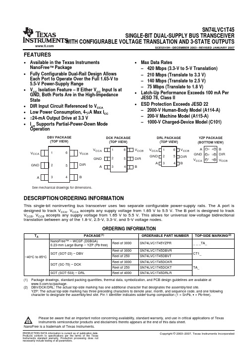
LOW POWER SCHOTTKYDevice Package Shipping SN74LS240N 16 Pin DIP 1440 Units/Box SN74LS240DW 16 Pin SOIC DW SUFFIX CASE 751D2500/T ape & Reel PLASTIC N SUFFIX CASE 738201201SN74LS244N 16 Pin DIP 1440 Units/Box SN74LS244DW16 Pin2500/T ape & ReelON Semiconductor and are trademarks of Semiconductor Components Industries, LLC (SCILLC). SCILLC reserves the right to make changes without further notice to any products herein. SCILLC makes no warranty, representation or guarantee regarding the suitability of its products for any particular purpose, nor does SCILLC assume any liability arising out of the application or use of any product or circuit, and specifically disclaims any and all liability, including without limitation special, consequential or incidental damages. “Typical” parameters which may be provided in SCILLC data sheets and/or specifications can and do vary in different applications and actual performance may vary over time. All operating parameters, including “Typicals” must be validated for each customer application by customer’s technical experts. SCILLC does not convey any license under its patent rights nor the rights of others.SCILLC products are not designed, intended, or authorized for use as components in systems intended for surgical implant into the body, or other applications intended to support or sustain life, or for any other application in which the failure of the SCILLC product could create a situation where personal injury or death may occur. Should Buyer purchase or use SCILLC products for any such unintended or unauthorized application, Buyer shall indemnify and hold SCILLC and its officers, employees, subsidiaries, affiliates, and distributors harmless against all claims, costs, damages, and expenses, and reasonable attorney fees arising out of, directly or indirectly, any claim of personal injury or death associated with such unintended or unauthorized use, even if such claim alleges that SCILLC was negligent regarding the design or manufacture of the part. SCILLC is an Equal Opportunity/Affirmative Action Employer. PUBLICATION ORDERING INFORMATIONASIA/PACIFIC: LDC for ON Semiconductor – Asia SupportPhone:303–675–2121 (Tue–Fri 9:00am to 1:00pm, Hong Kong Time)Toll Free from Hong Kong 800–4422–3781Email: ONlit–asia@JAPAN: ON Semiconductor, Japan Customer Focus Center4–32–1 Nishi–Gotanda, Shinagawa–ku, Tokyo, Japan 141–8549Phone: 81–3–5487–8345Email: r14153@Fax Response Line:303–675–2167。
HD74ALVC2G240US资料

Item Propagation delay time Enable time Disable time
•
VCC = 1.5±0.1 V
Symbol tPLH tPHL tZH tZL tHZ tLZ Min 2.0 2.0 2.0 Typ Max 7.0 7.0 7.0 Unit ns ns ns Test conditions CL = 15 pF CL = 15 pF CL = 15 pF FROM (Input) A OE OE TO (Output) Y Y Y
Rev.1, Jan. 2002, page 5 of 13
HD74ALVC2G240
Switching Characteristics
(Ta = −40 to 85°C) • VCC = 1.2 V
Symbol tPLH tPHL tZH tZL tHZ tLZ Min Typ 5.5 6.5 4.5 Max Unit ns ns ns Test conditions CL = 15 pF CL = 15 pF CL = 15 pF FROM (Input) A OE OE TO (Output) Y Y Y
mA mA mA mA mW °C
VI < 0 VO < 0 or VO > VCC VO = 0 to VCC
The absolute maximum ratings are values which must not individually be exceeded, and furthermore, no two of which may be realized at the same time. 1. The input and output voltage ratings may be exceeded if the input and output clamp-current ratings are observed. 2. This value is limited to 4.6 V maximum. 3. The maximum package power dissipation was calculated using a junction temperature of 150°C.
常见数字逻辑器件中文注解.pdf
常见数字逻辑器件中文注解型号器件名称厂牌SN7400四2输入端与非门SN7401四2输入端与非门(OC)SN7402四2输入端或非门TISN7403四2输入端与非门(OC)TISN7404六反相器TISN7405六反相器(OC)TISN7406六高压输出反相器(OC,30V)TISN7407六高压输出缓冲,驱动器(OC,30V)TISN7408四2输入端与门TISN7409四2输入端与门(OC)TISN7410三3输入端与非门TISN7412三3输入端与非门(OC)TISN7413双4输入端与非门TISN7414六反相器TISN7416六高压输出反相缓冲/驱动器TISN7417六高压输出缓冲/驱动器(OC,15V)TISN7420双4输入端与非门TISN7422双4输入端与非门(OC)TISN7423可扩展双4输入端或非门TISN7425双4输入端或非门TISN7426四2输入端高压输出与非缓冲器TISN7427三3输入端或非门TISN7428四2输入端或非缓冲器TISN74308输入端与非门TISN7432四2输入端或门74系列::74LS00TTL2输入端四与非门74LS01TTL集电极开路2输入端四与非门74LS02TTL2输入端四或非门74LS03TTL集电极开路2输入端四与非门74LS04TTL六反相器74LS05TTL集电极开路六反相器74LS06TTL集电极开路六反相高压驱动器74LS07TTL集电极开路六正相高压驱动器74LS08TTL2输入端四与门74LS09TTL集电极开路2输入端四与门74LS10TTL3输入端3与非门74LS107TTL带清除主从双J-K触发器74LS109TTL带预置清除正触发双J-K触发器74LS11TTL3输入端3与门74LS112TTL带预置清除负触发双J-K触发器74LS12TTL开路输出3输入端三与非门74LS121TTL单稳态多谐振荡器74LS122TTL可再触发单稳态多谐振荡器74LS123TTL双可再触发单稳态多谐振荡器74LS125TTL三态输出高有效四总线缓冲门74LS126TTL三态输出低有效四总线缓冲门74LS13TTL4输入端双与非施密特触发器74LS132TTL2输入端四与非施密特触发器74LS133TTL13输入端与非门74LS136TTL四异或门74LS138TTL3-8线译码器/复工器74LS139TTL双2-4线译码器/复工器74LS14TTL六反相施密特触发器74LS145TTL BCD—十进制译码/驱动器74LS15TTL开路输出3输入端三与门74LS150TTL16选1数据选择/多路开关74LS151TTL8选1数据选择器74LS153TTL双4选1数据选择器74LS154TTL4线—16线译码器74LS155TTL图腾柱输出译码器/分配器74LS156TTL开路输出译码器/分配器74LS157TTL同相输出四2选1数据选择器74LS158TTL反相输出四2选1数据选择器74LS16TTL开路输出六反相缓冲/驱动器74LS160TTL可预置BCD异步清除计数器74LS161TTL可予制四位二进制异步清除计数器74LS162TTL可预置BCD同步清除计数器74LS163TTL可予制四位二进制同步清除计数器74LS164TTL八位串行入/并行输出移位寄存器74LS165TTL八位并行入/串行输出移位寄存器74LS166TTL八位并入/串出移位寄存器74LS169TTL二进制四位加/减同步计数器74LS17TTL开路输出六同相缓冲/驱动器74LS170TTL开路输出4×4寄存器堆74LS173TTL三态输出四位D型寄存器74LS174TTL带公共时钟和复位六D触发器74LS175TTL带公共时钟和复位四D触发器74LS180TTL9位奇数/偶数发生器/校验器74LS181TTL算术逻辑单元/函数发生器74LS185TTL二进制—BCD代码转换器74LS190TTL BCD同步加/减计数器74LS191TTL二进制同步可逆计数器74LS192TTL可预置BCD双时钟可逆计数器74LS193TTL可预置四位二进制双时钟可逆计数器74LS194TTL四位双向通用移位寄存器74LS195TTL四位并行通道移位寄存器74LS196TTL十进制/二-十进制可预置计数锁存器74LS197TTL二进制可预置锁存器/计数器74LS20TTL4输入端双与非门74LS21TTL4输入端双与门74LS22TTL开路输出4输入端双与非门74LS221TTL双/单稳态多谐振荡器74LS240TTL八反相三态缓冲器/线驱动器74LS241TTL八同相三态缓冲器/线驱动器74LS243TTL四同相三态总线收发器74LS244TTL八同相三态缓冲器/线驱动器74LS245TTL八同相三态总线收发器74LS247TTL BCD—7段15V输出译码/驱动器74LS248TTL BCD—7段译码/升压输出驱动器74LS249TTL BCD—7段译码/开路输出驱动器74LS251TTL三态输出8选1数据选择器/复工器74LS253TTL三态输出双4选1数据选择器/复工器74LS256TTL双四位可寻址锁存器74LS257TTL三态原码四2选1数据选择器/复工器74LS258TTL三态反码四2选1数据选择器/复工器74LS259TTL八位可寻址锁存器/3-8线译码器74LS26TTL2输入端高压接口四与非门74LS260TTL5输入端双或非门74LS266TTL2输入端四异或非门74LS27TTL3输入端三或非门74LS273TTL带公共时钟复位八D触发器74LS279TTL四图腾柱输出S-R锁存器74LS28TTL2输入端四或非门缓冲器74LS283TTL4位二进制全加器74LS290TTL二/五分频十进制计数器74LS293TTL二/八分频四位二进制计数器74LS295TTL四位双向通用移位寄存器74LS298TTL四2输入多路带存贮开关74LS299TTL三态输出八位通用移位寄存器74LS30TTL8输入端与非门74LS32TTL2输入端四或门74LS322TTL带符号扩展端八位移位寄存器74LS323TTL三态输出八位双向移位/存贮寄存器74LS33TTL开路输出2输入端四或非缓冲器74LS347TTL BCD—7段译码器/驱动器74LS352TTL双4选1数据选择器/复工器74LS353TTL三态输出双4选1数据选择器/复工器74LS365TTL门使能输入三态输出六同相线驱动器74LS365TTL门使能输入三态输出六同相线驱动器74LS366TTL门使能输入三态输出六反相线驱动器74LS367TTL4/2线使能输入三态六同相线驱动器74LS368TTL4/2线使能输入三态六反相线驱动器74LS37TTL开路输出2输入端四与非缓冲器74LS373TTL三态同相八D锁存器74LS374TTL三态反相八D锁存器74LS375TTL4位双稳态锁存器74LS377TTL单边输出公共使能八D锁存器74LS378TTL单边输出公共使能六D锁存器74LS379TTL双边输出公共使能四D锁存器74LS38TTL开路输出2输入端四与非缓冲器74LS380TTL多功能八进制寄存器74LS39TTL开路输出2输入端四与非缓冲器74LS390TTL双十进制计数器74LS393TTL双四位二进制计数器74LS40TTL4输入端双与非缓冲器74LS42TTL BCD—十进制代码转换器74LS352TTL双4选1数据选择器/复工器74LS353TTL三态输出双4选1数据选择器/复工器74LS365TTL门使能输入三态输出六同相线驱动器74LS366TTL门使能输入三态输出六反相线驱动器74LS367TTL4/2线使能输入三态六同相线驱动器74LS368TTL4/2线使能输入三态六反相线驱动器74LS37TTL开路输出2输入端四与非缓冲器74LS373TTL三态同相八D锁存器74LS374TTL三态反相八D锁存器74LS375TTL4位双稳态锁存器74LS377TTL单边输出公共使能八D锁存器74LS378TTL单边输出公共使能六D锁存器74LS379TTL双边输出公共使能四D锁存器74LS38TTL开路输出2输入端四与非缓冲器74LS380TTL多功能八进制寄存器74LS39TTL开路输出2输入端四与非缓冲器74LS390TTL双十进制计数器74LS393TTL双四位二进制计数器74LS40TTL4输入端双与非缓冲器74LS42TTL BCD—十进制代码转换器74LS447TTL BCD—7段译码器/驱动器74LS45TTL BCD—十进制代码转换/驱动器74LS450TTL16:1多路转接复用器多工器74LS451TTL双8:1多路转接复用器多工器74LS453TTL四4:1多路转接复用器多工器74LS46TTL BCD—7段低有效译码/驱动器74LS460TTL十位比较器74LS461TTL八进制计数器74LS465TTL三态同相2与使能端八总线缓冲器74LS466TTL三态反相2与使能八总线缓冲器74LS467TTL三态同相2使能端八总线缓冲器74LS468TTL三态反相2使能端八总线缓冲器74LS469TTL八位双向计数器74LS47TTL BCD—7段高有效译码/驱动器74LS48TTL BCD—7段译码器/内部上拉输出驱动74LS490TTL双十进制计数器74LS491TTL十位计数器74LS498TTL八进制移位寄存器74LS50TTL2-3/2-2输入端双与或非门74LS502TTL八位逐次逼近寄存器74LS503TTL八位逐次逼近寄存器74LS51TTL2-3/2-2输入端双与或非门74LS533TTL三态反相八D锁存器74LS534TTL三态反相八D锁存器74LS54TTL四路输入与或非门74LS540TTL八位三态反相输出总线缓冲器74LS55TTL4输入端二路输入与或非门74LS563TTL八位三态反相输出触发器74LS564TTL八位三态反相输出D触发器74LS573TTL八位三态输出触发器74LS574TTL八位三态输出D触发器74LS645TTL三态输出八同相总线传送接收器74LS670TTL三态输出4×4寄存器堆74LS73TTL带清除负触发双J-K触发器74LS74TTL带置位复位正触发双D触发器74LS76TTL带预置清除双J-K触发器74LS83TTL四位二进制快速进位全加器74LS85TTL四位数字比较器74LS86TTL2输入端四异或门74LS90TTL可二/五分频十进制计数器74LS93TTL可二/八分频二进制计数器74LS95TTL四位并行输入\\输出移位寄存器74LS97TTL6位同步二进制乘法器CD系列::CD4000双3输入端或非门+单非门TICD4001四2输入端或非门HIT/NSC/TI/GOLCD4002双4输入端或非门NSCCD400618位串入/串出移位寄存器NSCCD4007双互补对加反相器NSCCD40084位超前进位全加器NSCCD4009六反相缓冲/变换器NSCCD4010六同相缓冲/变换器NSCCD4011四2输入端与非门HIT/TICD4012双4输入端与非门NSCCD4013双主-从D型触发器FSC/NSC/TOSCD40148位串入/并入-串出移位寄存器NSCCD4015双4位串入/并出移位寄存器TICD4016四传输门FSC/TICD4017十进制计数/分配器FSC/TI/MOTCD4018可预制1/N计数器NSC/MOTCD4019四与或选择器PHICD402014级串行二进制计数/分频器FSCCD402108位串入/并入-串出移位寄存器PHI/NSCCD4022八进制计数/分配器NSC/MOTCD4023三3输入端与非门NSC/MOT/TICD40247级二进制串行计数/分频器NSC/MOT/TICD4025三3输入端或非门NSC/MOT/TICD4026十进制计数/7段译码器NSC/MOT/TICD4027双J-K触发器NSC/MOT/TICD4028BCD码十进制译码器NSC/MOT/TICD4029可预置可逆计数器NSC/MOT/TICD4030四异或门NSC/MOT/TI/GOLCD403164位串入/串出移位存储器NSC/MOT/TICD4032三串行加法器NSC/TICD4033十进制计数/7段译码器NSC/TICD40348位通用总线寄存器NSC/MOT/TICD40354位并入/串入-并出/串出移位寄存NSC/MOT/TI CD4038三串行加法器NSC/TICD404012级二进制串行计数/分频器NSC/MOT/TICD4041四同相/反相缓冲器NSC/MOT/TICD4042四锁存D型触发器NSC/MOT/TICD40434三态R-S锁存触发器("1"触发)NSC/MOT/TI CD4044四三态R-S锁存触发器("0"触发)NSC/MOT/TI CD4046锁相环NSC/MOT/TI/PHICD4047无稳态/单稳态多谐振荡器NSC/MOT/TICD40484输入端可扩展多功能门NSC/HIT/TICD4049六反相缓冲/变换器NSC/HIT/TICD4050六同相缓冲/变换器NSC/MOT/TICD4051八选一模拟开关NSC/MOT/TICD4052双4选1模拟开关NSC/MOT/TICD4053三组二路模拟开关NSC/MOT/TICD4054液晶显示驱动器NSC/HIT/TICD4055BCD-7段译码/液晶驱动器NSC/HIT/TI CD4056液晶显示驱动器NSC/HIT/TICD4059“N”分频计数器NSC/TICD406014级二进制串行计数/分频器NSC/TI/MOT CD4063四位数字比较器NSC/HIT/TICD4066四传输门NSC/TI/MOTCD406716选1模拟开关NSC/TICD4068八输入端与非门/与门NSC/HIT/TICD4069六反相器NSC/HIT/TICD4070四异或门NSC/HIT/TICD4071四2输入端或门NSC/TICD4072双4输入端或门NSC/TICD4073三3输入端与门NSC/TICD4075三3输入端或门NSC/TICD4076四D寄存器CD4077四2输入端异或非门HITCD40788输入端或非门/或门CD4081四2输入端与门NSC/HIT/TICD4082双4输入端与门NSC/HIT/TICD4085双2路2输入端与或非门CD4086四2输入端可扩展与或非门CD4089二进制比例乘法器CD4093四2输入端施密特触发器NSC/MOT/ST CD40948位移位存储总线寄存器NSC/TI/PHICD40953输入端J-K触发器CD40963输入端J-K触发器CD4097双路八选一模拟开关CD4098双单稳态触发器NSC/MOT/TICD40998位可寻址锁存器NSC/MOT/STCD4010032位左/右移位寄存器CD401019位奇偶较验器CD401028位可预置同步BCD减法计数器CD401038位可预置同步二进制减法计数器CD401044位双向移位寄存器CD40105先入先出FI-FD寄存器CD40106六施密特触发器NSC\\TICD40107双2输入端与非缓冲/驱动器HAR\\TICD401084字×4位多通道寄存器CD40109四低-高电平位移器CD40110十进制加/减,计数,锁存,译码驱动STCD4014710-4线编码器NSC\\MOTCD40160可预置BCD加计数器NSC\\MOTCD40161可预置4位二进制加计数器NSC\\MOTCD40162BCD加法计数器NSC\\MOTCD401634位二进制同步计数器NSC\\MOTCD40174六锁存D型触发器NSC\\TI\\MOTCD40175四D型触发器NSC\\TI\\MOTCD401814位算术逻辑单元/函数发生器CD40182超前位发生器CD40192可预置BCD加/减计数器(双时钟)NSC\\TI CD40193可预置4位二进制加/减计数器NSC\\TICD401944位并入/串入-并出/串出移位寄存NSC\\MOT CD401954位并入/串入-并出/串出移位寄存NSC\\MOT CD402084×4多端口寄存器CD45014输入端双与门及2输入端或非门CD4502可选通三态输出六反相/缓冲器CD4503六同相三态缓冲器CD4504六电压转换器CD4506双二组2输入可扩展或非门CD4508双4位锁存D型触发器CD4510可预置BCD码加/减计数器CD4511BCD锁存,7段译码,驱动器CD4512八路数据选择器CD4513BCD锁存,7段译码,驱动器(消隐)CD45144位锁存,4线-16线译码器CD45154位锁存,4线-16线译码器CD4516可预置4位二进制加/减计数器CD4517双64位静态移位寄存器CD4518双BCD同步加计数器CD4519四位与或选择器CD4520双4位二进制同步加计数器CD452124级分频器CD4522可预置BCD同步1/N计数器CD4526可预置4位二进制同步1/N计数器CD4527BCD比例乘法器CD4528双单稳态触发器CD4529双四路/单八路模拟开关CD4530双5输入端优势逻辑门CD453112位奇偶校验器CD45328位优先编码器CD4536可编程定时器CD4538精密双单稳CD4539双四路数据选择器CD4541可编程序振荡/计时器CD4543BCD七段锁存译码,驱动器CD4544BCD七段锁存译码,驱动器CD4547BCD七段译码/大电流驱动器CD4549函数近似寄存器CD4551四2通道模拟开关CD4553三位BCD计数器CD4555双二进制四选一译码器/分离器CD4556双二进制四选一译码器/分离器CD4558BCD八段译码器CD4560"N"BCD加法器CD4561"9"求补器CD4573四可编程运算放大器CD4574四可编程电压比较器CD4575双可编程运放/比较器CD4583双施密特触发器CD4584六施密特触发器CD45854位数值比较器CD45998位可寻址锁存器74系列芯片功能大全7400TTL2输入端四与非门7401TTL集电极开路2输入端四与非门7402TTL2输入端四或非门7403TTL集电极开路2输入端四与非门7404TTL六反相器7405TTL集电极开路六反相器7406TTL集电极开路六反相高压驱动器7407TTL集电极开路六正相高压驱动器7408TTL2输入端四与门7409TTL集电极开路2输入端四与门7410TTL3输入端3与非门74107TTL带清除主从双J-K触发器74109TTL带预置清除正触发双J-K触发器7411TTL3输入端3与门74112TTL带预置清除负触发双J-K触发器7412TTL开路输出3输入端三与非门74121TTL单稳态多谐振荡器74122TTL可再触发单稳态多谐振荡器74123TTL双可再触发单稳态多谐振荡器74125TTL三态输出高有效四总线缓冲门74126TTL三态输出低有效四总线缓冲门7413TTL4输入端双与非施密特触发器74132TTL2输入端四与非施密特触发器74133TTL13输入端与非门74136TTL四异或门74138TTL3-8线译码器/复工器74139TTL双2-4线译码器/复工器7414TTL六反相施密特触发器74145TTL BCD—十进制译码/驱动器7415TTL开路输出3输入端三与门74150TTL16选1数据选择/多路开关74151TTL8选1数据选择器74153TTL双4选1数据选择器74154TTL4线—16线译码器74155TTL图腾柱输出译码器/分配器74156TTL开路输出译码器/分配器74157TTL同相输出四2选1数据选择器74158TTL反相输出四2选1数据选择器7416TTL开路输出六反相缓冲/驱动器74160TTL可预置BCD异步清除计数器74161TTL可予制四位二进制异步清除计数器74162TTL可预置BCD同步清除计数器74163TTL可予制四位二进制同步清除计数器74164TTL八位串行入/并行输出移位寄存器74165TTL八位并行入/串行输出移位寄存器74166TTL八位并入/串出移位寄存器74169TTL二进制四位加/减同步计数器7417TTL开路输出六同相缓冲/驱动器74170TTL开路输出4×4寄存器堆74173TTL三态输出四位D型寄存器74174TTL带公共时钟和复位六D触发器74175TTL带公共时钟和复位四D触发器74180TTL9位奇数/偶数发生器/校验器74181TTL算术逻辑单元/函数发生器74185TTL二进制—BCD代码转换器74190TTL BCD同步加/减计数器74191TTL二进制同步可逆计数器74192TTL可预置BCD双时钟可逆计数器74193TTL可预置四位二进制双时钟可逆计数器74194TTL四位双向通用移位寄存器74195TTL四位并行通道移位寄存器74196TTL十进制/二-十进制可预置计数锁存器74197TTL二进制可预置锁存器/计数器7420TTL4输入端双与非门7421TTL4输入端双与门7422TTL开路输出4输入端双与非门74221TTL双/单稳态多谐振荡器74240TTL八反相三态缓冲器/线驱动器74241TTL八同相三态缓冲器/线驱动器74243TTL四同相三态总线收发器74244TTL八同相三态缓冲器/线驱动器74245TTL八同相三态总线收发器74247TTL BCD—7段15V输出译码/驱动器74248TTL BCD—7段译码/升压输出驱动器74249TTL BCD—7段译码/开路输出驱动器74251TTL三态输出8选1数据选择器/复工器74253TTL三态输出双4选1数据选择器/复工器74256TTL双四位可寻址锁存器74257TTL三态原码四2选1数据选择器/复工器74258TTL三态反码四2选1数据选择器/复工器74259TTL八位可寻址锁存器/3-8线译码器7426TTL2输入端高压接口四与非门74260TTL5输入端双或非门74266TTL2输入端四异或非门7427TTL3输入端三或非门74273TTL带公共时钟复位八D触发器74279TTL四图腾柱输出S-R锁存器7428TTL2输入端四或非门缓冲器74283TTL4位二进制全加器74290TTL二/五分频十进制计数器74293TTL二/八分频四位二进制计数器74295TTL四位双向通用移位寄存器74298TTL四2输入多路带存贮开关74299TTL三态输出八位通用移位寄存器7430TTL8输入端与非门7432TTL2输入端四或门74322TTL带符号扩展端八位移位寄存器74323TTL三态输出八位双向移位/存贮寄存器7433TTL开路输出2输入端四或非缓冲器74347TTL BCD—7段译码器/驱动器74352TTL双4选1数据选择器/复工器74353TTL三态输出双4选1数据选择器/复工器74365TTL门使能输入三态输出六同相线驱动器74365TTL门使能输入三态输出六同相线驱动器74366TTL门使能输入三态输出六反相线驱动器74367TTL4/2线使能输入三态六同相线驱动器74368TTL4/2线使能输入三态六反相线驱动器7437TTL开路输出2输入端四与非缓冲器74373TTL三态同相八D锁存器74374TTL三态反相八D锁存器74375TTL4位双稳态锁存器74377TTL单边输出公共使能八D锁存器74378TTL单边输出公共使能六D锁存器74379TTL双边输出公共使能四D锁存器7438TTL开路输出2输入端四与非缓冲器74380TTL多功能八进制寄存器7439TTL开路输出2输入端四与非缓冲器74390TTL双十进制计数器74393TTL双四位二进制计数器7440TTL4输入端双与非缓冲器7442TTL BCD—十进制代码转换器74352TTL双4选1数据选择器/复工器74353TTL三态输出双4选1数据选择器/复工器74365TTL门使能输入三态输出六同相线驱动器74366TTL门使能输入三态输出六反相线驱动器74367TTL4/2线使能输入三态六同相线驱动器74368TTL4/2线使能输入三态六反相线驱动器7437TTL开路输出2输入端四与非缓冲器74373TTL三态同相八D锁存器74374TTL三态反相八D锁存器74375TTL4位双稳态锁存器74377TTL单边输出公共使能八D锁存器74378TTL单边输出公共使能六D锁存器74379TTL双边输出公共使能四D锁存器7438TTL开路输出2输入端四与非缓冲器74380TTL多功能八进制寄存器7439TTL开路输出2输入端四与非缓冲器74390TTL双十进制计数器74393TTL双四位二进制计数器7440TTL4输入端双与非缓冲器7442TTL BCD—十进制代码转换器74447TTL BCD—7段译码器/驱动器7445TTL BCD—十进制代码转换/驱动器74450TTL16:1多路转接复用器多工器74451TTL双8:1多路转接复用器多工器74453TTL四4:1多路转接复用器多工器7446TTL BCD—7段低有效译码/驱动器74460TTL十位比较器74461TTL八进制计数器74465TTL三态同相2与使能端八总线缓冲器74466TTL三态反相2与使能八总线缓冲器74467TTL三态同相2使能端八总线缓冲器74468TTL三态反相2使能端八总线缓冲器74469TTL八位双向计数器7447TTL BCD—7段高有效译码/驱动器7448TTL BCD—7段译码器/内部上拉输出驱动74490TTL双十进制计数器74491TTL十位计数器74498TTL八进制移位寄存器7450TTL2-3/2-2输入端双与或非门74502TTL八位逐次逼近寄存器74503TTL八位逐次逼近寄存器7451TTL2-3/2-2输入端双与或非门74533TTL三态反相八D锁存器74534TTL三态反相八D锁存器7454TTL四路输入与或非门74540TTL八位三态反相输出总线缓冲器7455TTL4输入端二路输入与或非门74563TTL八位三态反相输出触发器74564TTL八位三态反相输出D触发器74573TTL八位三态输出触发器74574TTL八位三态输出D触发器74645TTL三态输出八同相总线传送接收器74670TTL三态输出4×4寄存器堆7473TTL带清除负触发双J-K触发器7474TTL带置位复位正触发双D触发器7476TTL带预置清除双J-K触发器7483TTL四位二进制快速进位全加器7485TTL四位数字比较器7486TTL2输入端四异或门7490TTL可二/五分频十进制计数器7493TTL可二/八分频二进制计数器7495TTL四位并行输入\\输出移位寄存器7497TTL6位同步二进制乘法器CD系列门电路CD4000双3输入端或非门CD4001四2输入端或非门CD4002双4输入端或非门CD4007双互补对加反向器CD4009六反向缓冲/变换器CD4011四2输入端与非门CD4012双4输入端与非门CD4023三2输入端与非门CD4025三2输入端与非门CD4030四2输入端异或门CD4041四同相/反向缓冲器CD40488输入端可扩展多功能门CD4049六反相缓冲/变换器CD4050六同相缓冲/变换器CD40688输入端与门/与非门CD4069六反相器CD4070四2输入异或门CD4071四2输入端或门CD4072双4输入端或门CD4073三3输入端与门CD4075三3输入端或门CD4077四异或非门CD40788输入端与非门/或门CD4081四2输入端与门CD4082双4输入端与非门CD4085双2路2输入端与或非门CD4086四2输入端可扩展与或非门CD40104TTL至高电平CMOS转换器CD40106六施密特触发器CD40107双2输入端与非缓冲/驱动器CD40109四低-高电平位移器CD4501三多输入门CD4052六反向缓冲器(三态输出)CD4503六同相缓冲器(三态输出)CD45046TTL或CMOS同级移相器CD4506双可扩展AIO门CD4507四异或门CD45194位与/或选择器CD4530双5输入多数逻辑门CD4572四反向器加二输入或非门加二输入与非门CD45998位可寻址锁存器触发器CD4013双D触发器CD4027双JK触发器CD4042四锁存D型触发器CD4043四三态R-S锁存触发器(“1”触发)CD4044四三态R-S锁存触发器(“0”触发)CD4047单稳态触发/无稳多谐振荡器CD4093四2输入端施密特触发器CD4098双单稳态触发器CD40998位可寻址锁存器CD4508双4位锁存触发器CD4528双单稳态触发器(与CD4098管脚相同,只是3、13脚复位开关为高电平有效)CD4538精密单稳多谐振荡器CD4583双施密特触发器CD4584六施密特触发器CD45998位可寻址锁存器计数器CD4017十进制计数/分配器CD402014位二进制串行计数器/分频器CD4022八进制计数/分配器CD40247位二进制串行计数器/分频器CD4029可预置数可逆计数器(4位二进制或BCD码)CD404012二进制串行计数器/分频器CD404512位计数/缓冲器CD4059四十进制N分频器CD406014二进制串行计数器/分频器和振荡器CD40953输入端J-K触发器(相同J-K输入端)CD40963输入端J-K触发器(相反和相同J-K输入端)CD40110十进制加/减计数/锁存/7端译码/驱动器CD40160可预置数BCD加计数器(异步复位)CD40161可预置数4位二进制加计数器(R非=0时,CP上脉冲复位)(异步复位)CD40162可预置数BCD加计数器(同步复位)CD40163可预置数4位二进制加计数器(R非=0时,CP上脉冲复位)(同步复位)CD40192可预置数BCD加/减计数器CD40193可预置数4位二进制加/减计数器CD4510可预置BCD加/减计数器CD4516可预置4位二进制加/减计数器CD4518双BCD同步加计数器CD4520双同步4位二进制加计数器CD452124级频率分频器CD4522可预置数BCD同步1/N加计数器CD4526可预置数4位二进制同步1/N加计数器CD4534实时与译码计数器CD4536可编程定时器CD4541可编程定时器CD45533数字BCD计数器CD4568相位比较器/可编程计数器CD4569双可预置BCD/二进制计数器CD45978位总线相容计数/锁存器CD45988位总线相容可建地址锁存器译码器CD4511BCD锁存/7段译码器/驱动器CD45144位锁存/4-16线译码器CD45154位锁存/4-16线译码器(负逻辑输出)CD4026十进制计数/7段译码器(适用于时钟计时电路,利用C端的功能可方便的实现60或12分CD4028BCD-十进制译码器CD4033十进制计数/7段译码器CD40544位液晶显示驱动CD4055BCD-7段码/液晶驱动CD4056BCD-7段码/驱动CD401028位可预置同步减法计时器(BCD)CD401038位可预置同步减法计时器(二进制)CD4513BCD-锁存/7端译码/驱动器(无效“0”不显)CD45144位锁存/4线—16线译码器(输出“1”)CD45154位锁存/4线—16线译码器(输出“0”)CD4543BCD-锁存/7段译码/驱动器CD4544BCD-锁存/7段译码/驱动器——波动闭锁CD4547BCD-锁存/7段译码/大电流驱动器CD4555双二进制4选1译码器/分离器(输出“1”)CD4556双二进制4选1译码器/分离器(输出“0”)CD4558BCD-7段译码CD4555双二进制4选1译码器/分离器CD4556双二进制4选1译码器/分离器(负逻辑输出)移位寄存器CD400618位串入—串出移位寄存器CD40148位串入/并入—串出移位寄存器CD4015双4位串入—并出移位寄存器CD40218位串入/并入—串出移位寄存器CD403164位移位寄存器CD40348位通用总线寄存器CD40354位串入/并入—串出/并出移位寄存器CD40764线D型寄存器CD40948位移位/存储总线寄存器CD4010032位左移/右移CD40105先进先出寄存器CD401084×4多端口寄存器阵列CD401944位并入/串入—并出/串出移位寄存器(左移/右移)CD401954位并入/串入—并出/串出移位寄存器CD451764位移位寄存器CD45490连续的近似值寄存器CD4562128位静态移位寄存器CD45804×4多端寄存器模拟开关和数据选择器CD4016四联双向开关CD4019四与或选择器【Qn=(An*Ka)+(Bn*Kb)】CD4051单八路模拟开关CD4052双4路模拟开关CD4053三2路模拟开关CD4066四双向模拟开关CD4067单十六路模拟开关CD4097双八路模拟开关CD40257四2选1数据选择器CD4512八路数据选择器CD4529双四路/单八路模拟开关CD4539双四路数据选择器CD4551四2通道模拟多路传输运算电路CD40084位超前进位全加器CD4019四与或选择器【Qn=(An*Ka)+(Bn*Kb)】CD4527BCD比例乘法器CD4032三路串联加法器CD4038三路串联加法器(负逻辑)CD4063四位量级比较器CD4070四2输入异或门CD45854位数值比较器CD40894位二进制比例乘法器CD401019位奇偶发生器/校验器CD4527BCD比例乘法器CD453112位奇偶数CD4559逐次近似值码器CD4560“N”BCD加法器CD4561“9”求补器CD45814位算术逻辑单元CD4582超前进位发生器CD45854位数值比较器存储器CD40494字×8位随机存取存储器CD450564×1位RAMCD4537256×1静态随机存取存储器CD4552256位RAM特殊电路CD4046锁相环集成电路CD45328位优先编码器CD4500工业控制单元CD4566工业时基发生器CD4573可预置运算放大器CD4574比较器、线性、双对双运放CD4575双/双预置运放/比较器CD45978位总线相容计数/锁存器CD45988位总线相容可建地址锁存器。
SN74LVC1T45DCKRE4中文资料
FEATURESV CCA V CCBBGNDADBV PACKAGE(TOP VIEW)DCK PACKAGE(TOP VIEW)V CCA V CCBBAV CCBDRL PACKAGE(TOP VIEW)See mechanical drawings for dimensions.DIRDIRYZP PACKAGE(BOTTOM VIEW)V CCAAV CCBBGND DIR DESCRIPTION/ORDERING INFORMATIONWITH CONFIGURABLE VOLTAGE TRANSLATION AND3-STATE OUTPUTSSCES515H–DECEMBER2003–REVISED JANUARY2007•Available in the Texas Instruments•Max Data RatesNanoFree™Package–420Mbps(3.3-V to5-V Translation)•Fully Configurable Dual-Rail Design Allows–210Mbps(Translate to3.3V) Each Port to Operate Over the Full1.65-V to–140Mbps(Translate to2.5V)5.5-V Power-Supply Range–75Mbps(Translate to1.8V)•V CC Isolation Feature–If Either V CC Input Is at•Latch-Up Performance Exceeds100mA Per GND,Both Ports Are in the High-ImpedanceJESD78,Class IIState•ESD Protection Exceeds JESD22•DIR Input Circuit Referenced to V CCA–2000-V Human-Body Model(A114-A)•Low Power Consumption,4-µA Max I CC–200-V Machine Model(A115-A)•±24-mA Output Drive at3.3V–1000-V Charged-Device Model(C101)•I off Supports Partial-Power-Down ModeOperationThis single-bit noninverting bus transceiver uses two separate configurable power-supply rails.The A port is designed to track V CCA.V CCA accepts any supply voltage from1.65V to5.5V.The B port is designed to track V CCB.V CCB accepts any supply voltage from1.65V to5.5V.This allows for universal low-voltage bidirectional translation between any of the1.8-V,2.5-V,3.3-V,and5-V voltage nodes.ORDERING INFORMATIONT A PACKAGE(1)ORDERABLE PART NUMBER TOP-SIDE MARKING(2)NanoFree™–WCSP(DSBGA)Reel of3000SN74LVC1T45YZPR___TA_0.23-mm Large Bump–YZP(Pb-free)Reel of3000SN74LVC1T45DBVRSOT(SOT-23)–DBV CT1_Reel of250SN74LVC1T45DBVT–40°C to85°CReel of3000SN74LVC1T45DCKRSOT(SC-70)–DCKReel of250SN74LVC1T45DCKT TA_SOT(SOT-533)–DRL Reel of4000SN74LVC1T45DRLR(1)Package drawings,standard packing quantities,thermal data,symbolization,and PCB design guidelines are available at/sc/package.(2)DBV/DCK/DRL:The actual top-side marking has one additional character that designates the assembly/test site.YZP:The actual top-side marking has three preceding characters to denote year,month,and sequence code,and one following character to designate the assembly/test site.Pin1identifier indicates solder-bump composition(1=SnPb,•=Pb-free).Please be aware that an important notice concerning availability,standard warranty,and use in critical applications of TexasInstruments semiconductor products and disclaimers thereto appears at the end of this data sheet.NanoFree is a trademark of Texas Instruments.PRODUCTION DATA information is current as of publication date.Copyright©2003–2007,Texas Instruments Incorporated Products conform to specifications per the terms of the TexasInstruments standard warranty.Production processing does notnecessarily include testing of all parameters.DESCRIPTION/ORDERING INFORMATION (CONTINUED)BDIRAV CCA V CCBWITH CONFIGURABLE VOLTAGE TRANSLATION AND 3-STATE OUTPUTSSCES515H–DECEMBER 2003–REVISED JANUARY 2007The SN74LVC1T45is designed for asynchronous communication between two data buses.The logic levels of the direction-control (DIR)input activate either the B-port outputs or the A-port outputs.The device transmits data from the A bus to the B bus when the B-port outputs are activated and from the B bus to the A bus when the A-port outputs are activated.The input circuitry on both A and B ports always is active and must have a logic HIGH or LOW level applied to prevent excess I CC and I CCZ .The SN74LVC1T45is designed so that the DIR input is powered by V CCA .This device is fully specified for partial-power-down applications using I off .The I off circuitry disables the outputs,preventing damaging current backflow through the device when it is powered down.The V CC isolation feature ensures that if either V CC input is at GND,then both ports are in the high-impedance state.NanoFree™package technology is a major breakthrough in IC packaging concepts,using the die as the package.FUNCTION TABLE (1)INPUT OPERATION DIR L B data to A bus HA data toB bus(1)Input circuits of the data I/Os always are active.LOGIC DIAGRAM (POSITIVE LOGIC)2Submit Documentation FeedbackAbsolute Maximum Ratings (1)WITH CONFIGURABLE VOLTAGE TRANSLATION AND 3-STATE OUTPUTSSCES515H–DECEMBER 2003–REVISED JANUARY 2007over operating free-air temperature range (unless otherwise noted)MINMAX UNIT V CCA Supply voltage range –0.5 6.5V V CCB V I Input voltage range (2)–0.5 6.5V V O Voltage range applied to any output in the high-impedance or power-off state (2)–0.5 6.5V A port –0.5V CCA +0.5V O Voltage range applied to any output in the high or low state (2)(3)V B port –0.5V CCB +0.5I IK Input clamp current V I <0–50mA I OK Output clamp current V O <0–50mA I OContinuous output current±50mA Continuous current through V CC or GND±100mADBV package165DCK package 259θJAPackage thermal impedance (4)°C/W DRL package 142YZP package123T stg Storage temperature range–65150°C (1)Stresses beyond those listed under "absolute maximum ratings"may cause permanent damage to the device.These are stress ratings only,and functional operation of the device at these or any other conditions beyond those indicated under "recommended operating conditions"is not implied.Exposure to absolute-maximum-rated conditions for extended periods may affect device reliability.(2)The input and output negative-voltage ratings may be exceeded if the input and output clamp-current ratings are observed.(3)The value of V CC is provided in the recommended operating conditions table.(4)The package thermal impedance is calculated in accordance with JESD 51-7.3Submit Documentation FeedbackRecommended Operating Conditions (1)(2)(3)WITH CONFIGURABLE VOLTAGE TRANSLATION AND 3-STATE OUTPUTSSCES515H–DECEMBER 2003–REVISED JANUARY 2007V CCIV CCOMIN MAX UNIT V CCA 1.65 5.5Supply voltageVV CCB1.655.51.65V to 1.95VV CCI ×0.652.3V to 2.7V 1.7High-level V IHData inputs (4)Vinput voltage3V to 3.6V 24.5V to5.5V V CCI ×0.71.65V to 1.95VV CCI ×0.352.3V to 2.7V 0.7Low-level V ILData inputs (4)V input voltage3V to 3.6V 0.84.5V to5.5V V CCI ×0.31.65V to 1.95VV CCA ×0.652.3V to 2.7V 1.7High-level DIRV IHVinput voltage(referenced to V CCA )(5)3V to 3.6V 24.5V to5.5V V CCA ×0.71.65V to 1.95VV CCA ×0.352.3V to 2.7V 0.7Low-level DIRV ILV input voltage (referenced to V CCA )(5)3V to 3.6V 0.84.5V to5.5VV CCA ×0.3V I Input voltage 0 5.5V V OOutput voltageV CCOV 1.65V to 1.95V–42.3V to 2.7V –8I OHHigh-level output currentmA 3V to 3.6V –244.5V to 5.5V –321.65V to 1.95V42.3V to 2.7V 8I OLLow-level output currentmA 3V to 3.6V 244.5V to 5.5V321.65V to 1.95V202.3V to 2.7V 20Data inputsInput transition ∆t/∆v3V to 3.6V 10ns/V rise or fall rate4.5V to5.5V5Control inputs1.65V to 5.5V5T A Operating free-air temperature–4085°C (1)V CCI is the V CC associated with the input port.(2)V CCO is the V CC associated with the output port.(3)All unused data inputs of the device must be held at V CCI or GND to ensure proper device operation.Refer to the TI application report,Implications of Slow or Floating CMOS Inputs ,literature number SCBA004.(4)For V CCI values not specified in the data sheet,V IH min =V CCI ×0.7V,V IL max =V CCI ×0.3V.(5)For V CCI values not specified in the data sheet,V IH min =V CCA ×0.7V,V IL max =V CCA ×0.3V.4Submit Documentation FeedbackElectrical Characteristics (1)(2)WITH CONFIGURABLE VOLTAGE TRANSLATION AND 3-STATE OUTPUTSSCES515H–DECEMBER 2003–REVISED JANUARY 2007over recommended operating free-air temperature range (unless otherwise noted)T A =25°C –40°C to 85°C PARAMETERTEST CONDITIONS V CCA V CCB UNITMINTYPMAXMIN MAXV CCO I OH =–100µA1.65V to 4.5V1.65V to 4.5V–0.1I OH =–4mA 1.65V 1.65V 1.2V OHV I =V IHVI OH =–8mA 2.3V 2.3V 1.9I OH =–24mA 3V 3V 2.4I OH =–32mA 4.5V 4.5V 3.8I OL =100µA 1.65V to 4.5V1.65V to 4.5V0.1I OL =4mA1.65V 1.65V 0.45V OLI OL =8mA V I =V IL 2.3V 2.3V 0.3V I OL =24mA 3V 3V 0.55I OL =32mA4.5V 4.5V 0.55I I DIR V I =V CCA or GND 1.65V to5.5V1.65V to 5.5V ±1±2µA A port 0V 0to 5.5V ±1±2I off V I or V O =0to 5.5V µA B port 0to 5.5V 0V ±1±2A or B I OZV O =V CCO or GND1.65V to 5.5V 1.65V to 5.5V ±1±2µA port1.65V to 5.5V1.65V to 5.5V3I CCAV I =V CCI or GND,I O =05.5V 0V 2µA 0V 5.5V -21.65V to 5.5V1.65V to 5.5V3I CCBV I =V CCI or GND,I O =05.5V 0V -2µA 0V5.5V 2I CCA +I CCB V I =V CCI or GND,I O =0 1.65V to 5.5V1.65V to 5.5V4µA (see Table 1)A port at V CCA –0.6V,A port50DIR at V CCA ,B port =open ∆I CCA3V to 5.5V3V to 5.5VµA DIR at V CCA –0.6V,DIRB port =open,50A port at V CCA or GNDB port at V CCB –0.6V,∆I CCB B port DIR at GND,3V to 5.5V 3V to 5.5V 50µA A port =openC i DIR V I =V CCA or GND 3.3V 3.3V 2.5pF A or B C io V O =V CCA/B or GND3.3V3.3V6pFport(1)V CCO is the V CC associated with the output port.(2)V CCI is the V CC associated with the input port.5Submit Documentation FeedbackSwitching CharacteristicsSwitching CharacteristicsWITH CONFIGURABLE VOLTAGE TRANSLATION AND 3-STATE OUTPUTSSCES515H–DECEMBER 2003–REVISED JANUARY 2007over recommended operating free-air temperature range,V CCA =1.8V ±0.15V (see Figure 1)V CCB =1.8V V CCB =2.5V V CCB =3.3V V CCB =5V FROM TO ±0.15V ±0.2V ±0.3V ±0.5V PARAMETERUNIT(INPUT)(OUTPUT)MIN MAX MIN MAX MIN MAX MIN MAX t PLH 317.7 2.210.3 1.78.3 1.47.2A B ns t PHL 2.814.3 2.28.5 1.87.1 1.77t PLH 317.7 2.316 2.115.5 1.915.1B A ns t PHL 2.814.3 2.112.9212.6 1.812.2t PHZ 5.219.4 4.818.5 4.718.4 5.117.1DIR A ns t PLZ 2.310.5 2.110.5 2.410.7 3.110.9t PHZ 7.421.9 4.911.5 4.610.3 2.88.2DIR B ns t PLZ 4.216 3.79.2 3.38.4 2.46.4t PZH (1)33.725.223.921.5DIR A ns t PZL (1)36.224.422.920.4t PZH (1)28.220.81918.1DIRBns t PZL (1)33.72725.524.1(1)The enable time is a calculated value,derived using the formula shown in the enable times section.over recommended operating free-air temperature range,V CCA =2.5V ±0.2V (see Figure 1)V CCB =1.8V V CCB =2.5V V CCB =3.3V V CCB =5V FROM TO ±0.15V ±0.2V ±0.3V ±0.5V PARAMETERUNIT(INPUT)(OUTPUT)MIN MAX MIN MAX MIN MAX MIN MAX t PLH 2.316 1.58.5 1.3 6.4 1.1 5.1A B ns t PHL 2.112.9 1.47.5 1.3 5.40.9 4.6t PLH 2.210.3 1.58.5 1.4817.5B A ns t PHL 2.28.5 1.47.5 1.370.9 6.2t PHZ 38.1 3.18.1 2.88.1 3.28.1DIR A ns t PLZ 1.3 5.9 1.3 5.9 1.3 5.91 5.8t PHZ 6.523.7 4.111.4 3.910.2 2.47.1DIR B ns t PLZ 3.918.9 3.29.6 2.88.4 1.85.3t PZH (1)29.218.116.412.8DIR A ns t PZL (1)32.218.917.213.3t PZH (1)21.914.412.310.9DIRBns t PZL (1)2115.613.512.7(1)The enable time is a calculated value,derived using the formula shown in the enable times section.6Submit Documentation FeedbackSwitching CharacteristicsSwitching CharacteristicsOperating CharacteristicsWITH CONFIGURABLE VOLTAGE TRANSLATION AND 3-STATE OUTPUTSSCES515H–DECEMBER 2003–REVISED JANUARY 2007over recommended operating free-air temperature range,V CCA =3.3V ±0.3V (see Figure 1)V CCB =1.8V V CCB =2.5V V CCB =3.3V V CCB =5V FROM TO ±0.15V ±0.2V ±0.3V ±0.5V PARAMETERUNIT(INPUT)(OUTPUT)MIN MAX MIN MAXMIN MAX MIN MAX t PLH 2.115.5 1.480.7 5.80.7 4.4A B ns t PHL 212.6 1.370.850.74t PLH 1.78.3 1.3 6.40.7 5.80.6 5.4B A ns t PHL 1.87.1 1.3 5.40.850.7 4.5t PHZ 2.97.337.3 2.87.3 3.47.3DIR A ns t PLZ 1.8 5.6 1.6 5.6 2.2 5.7 2.2 5.7t PHZ 5.420.5 3.910.1 2.98.8 2.4 6.8DIR B ns t PLZ 3.314.5 2.97.8 2.47.1 1.74.9t PZH (1)22.814.212.910.3DIR A ns t PZL (1)27.615.513.811.3t PZH (1)21.113.611.510.1DIRBns t PZL (1)19.914.312.311.3(1)The enable time is a calculated value,derived using the formula shown in the enable times section.over recommended operating free-air temperature range,V CCA =5V ±0.5V (see Figure 1)V CCB =1.8V V CCB =2.5V V CCB =3.3V V CCB =5V FROM TO ±0.15V ±0.2V ±0.3V ±0.5V PARAMETERUNIT(INPUT)(OUTPUT)MIN MAX MIN MAX MIN MAX MIN MAX t PLH 1.915.117.50.6 5.40.5 3.9A B ns t PHL 1.812.20.9 6.20.7 4.50.5 3.5t PLH 1.47.21 5.10.7 4.40.5 3.9B A ns t PHL 1.770.9 4.60.740.5 3.5t PHZ 2.1 5.4 2.2 5.4 2.2 5.5 2.2 5.4DIR A ns t PLZ 0.9 3.81 3.81 3.70.9 3.7t PHZ 4.820.2 2.59.818.5 2.5 6.5DIR B ns t PLZ 4.214.8 2.57.4 2.57 1.64.5t PZH (1)2212.511.48.4DIR A ns t PZL (1)27.214.412.510t PZH (1)18.911.39.17.6DIRBns t PZL (1)17.611.6108.6(1)The enable time is a calculated value,derived using the formula shown in the enable times section.T A =25°CV CCA =V CCA =V CCA =V CCA =TEST V CCB =1.8VV CCB =2.5VV CCB =3.3VV CCB =5VPARAMETERUNITCONDITIONS TYP TYP TYP TYP A-port input,B-port output C L =0pF,3444C pdA(1)f =10MHz,pF B-port input,A-port output 18192021t r =t f =1ns A-port input,B-port output C L =0pF,18192021C pdB (1)f =10MHz,pF B-port input,A-port output3444t r =t f =1ns(1)Power dissipation capacitance per transceiver7Submit Documentation FeedbackPower-Up ConsiderationsWITH CONFIGURABLE VOLTAGE TRANSLATION AND 3-STATE OUTPUTSSCES515H–DECEMBER 2003–REVISED JANUARY 2007A proper power-up sequence always should be followed to avoid excessive supply current,bus contention,oscillations,or other anomalies.To guard against such power-up problems,take the following precautions:1.Connect ground before any supply voltage is applied.2.Power up V CCA .3.V CCB can be ramped up along with or after V CCA .Table 1.Typical Total Static Power Consumption (I CCA +I CCB )V CCAV CCB UNIT0V 1.8V 2.5V 3.3V 5V 0V 0<1<1<1<11.8V <1<2<2<222.5V <1<2<2<2<2µA 3.3V <1<2<2<2<25V<12<2<2<28Submit Documentation FeedbackTYPICAL CHARACTERISTICSt P H L − n sC L − pF105101520253035t P L H− n s C L − pF5101520253035t P H L− n sC L − pF5101520253035t P L H − n sC L − pFWITH CONFIGURABLE VOLTAGE TRANSLATION AND 3-STATE OUTPUTSSCES515H–DECEMBER 2003–REVISED JANUARY 2007TYPICAL PROPAGATION DELAY (A to B)vs LOAD CAPACITANCET A =25°C,V CCA =1.8VTYPICAL PROPAGATION DELAY (B to A)vs LOAD CAPACITANCET A =25°C,V CCA =1.8V9Submit Documentation Feedback5101520253035t P H L − n sC L − pF5t P L H − n sC L − pFt P H L− n s C L − pF12345678910t P L H − n sC L − pFWITH CONFIGURABLE VOLTAGE TRANSLATION AND 3-STATE OUTPUTSSCES515H–DECEMBER 2003–REVISED JANUARY 2007TYPICAL CHARACTERISTICS (continued)TYPICAL PROPAGATION DELAY (A to B)vs LOAD CAPACITANCET A =25°C,V CCA =2.5VTYPICAL PROPAGATION DELAY (B to A)vs LOAD CAPACITANCET A =25°C,V CCA =2.5V10Submit Documentation Feedbackt P H L − n sC L − pFt P L H − n sC L − pFt P H L− n s C L − pFt P L H − n s C L − pFSN74LVC1T45SINGLE-BIT DUAL-SUPPLY BUS TRANSCEIVERWITH CONFIGURABLE VOLTAGE TRANSLATION AND 3-STATE OUTPUTSSCES515H–DECEMBER 2003–REVISED JANUARY 2007TYPICAL CHARACTERISTICS (continued)TYPICAL PROPAGATION DELAY (A to B)vs LOAD CAPACITANCET A =25°C,V CCA =3.3VTYPICAL PROPAGATION DELAY (B to A)vs LOAD CAPACITANCET A =25°C,V CCA =3.3Vt P H L− n s C L − pFt P L H − n s C L − pFt P H L − n sC L − pFt P L H − n sC L − pFSN74LVC1T45SINGLE-BIT DUAL-SUPPLY BUS TRANSCEIVERWITH CONFIGURABLE VOLTAGE TRANSLATION AND 3-STATE OUTPUTSSCES515H–DECEMBER 2003–REVISED JANUARY 2007TYPICAL CHARACTERISTICS (continued)TYPICAL PROPAGATION DELAY (A to B)vs LOAD CAPACITANCET A =25°C,V CCA =5VTYPICAL PROPAGATION DELAY (B to A)vs LOAD CAPACITANCET A =25°C,V CCA =5VPARAMETER MEASUREMENT INFORMATIONV OH V OLLOAD CIRCUIT × V CCOOpenOutput Control (low-level enabling)Output Waveform 1S1 at 2 × V CCO (see Note B)Output Waveform 2S1 at GND (see Note B)0 V0 VV CCI0 VV CCAV CCOVOLTAGE WAVEFORMS PROPAGATION DELAY TIMESVOLTAGE WAVEFORMS PULSE DURATIONVOLTAGE WAVEFORMS ENABLE AND DISABLE TIMESInputt pd t PLZ /t PZL t PHZ /t PZHOpen 2 × V CCO GNDTEST S1NOTES: A.C L includes probe and jig capacitance.B.Waveform 1 is for an output with internal conditions such that the output is low, except when disabled by the output control.Waveform 2 is for an output with internal conditions such that the output is high, except when disabled by the output control.C.All input pulses are supplied by generators having the following characteristics: PRR v 10 MHz, Z O = 50 Ω, dv/dt ≥ 1 V/ns.D.The outputs are measured one at a time, with one transition per measurement.E.t PLZ and t PHZ are the same as t dis .F.t PZL and t PZH are the same as t en .G.t PLH and t PHL are the same as t pd .H.V CCI is the V CC associated with the input port.I.V CCO is the V CC associated with the output port.J.All parameters and waveforms are not applicable to all devices.1.8 V ± 0.15 V2.5 V ± 0.2 V3.3 V ± 0.3 V 5 V ± 0.5 V2 k Ω2 k Ω2 k Ω2 k ΩV CCO R L 0.15 V 0.15 V 0.3 V 0.3 VV TP C L 15 pF 15 pF 15 pF 15 pFSN74LVC1T45SINGLE-BIT DUAL-SUPPLY BUS TRANSCEIVERWITH CONFIGURABLE VOLTAGE TRANSLATION AND 3-STATE OUTPUTSSCES515H–DECEMBER 2003–REVISED JANUARY 2007Figure 1.Load Circuit and Voltage WaveformsAPPLICATION INFORMATIONSYSTEM-1SYSTEM-2SN74LVC1T45SINGLE-BIT DUAL-SUPPLY BUS TRANSCEIVERWITH CONFIGURABLE VOLTAGE TRANSLATION AND 3-STATE OUTPUTSSCES515H–DECEMBER 2003–REVISED JANUARY 2007Figure 2shows an example of the SN74LVC1T45being used in a unidirectional logic level-shifting application.PIN NAME FUNCTION DESCRIPTION1V CCA V CC1SYSTEM-1supply voltage (1.65V to 5.5V)2GND GND Device GND3A OUT Output level depends on V CC1voltage.4B IN Input threshold value depends on V CC2voltage.5DIR DIR GND (low level)determines B-port to A-port direction.6V CCBV CC2SYSTEM-2supply voltage (1.65V to 5.5V)Figure 2.Unidirectional Logic Level-Shifting ApplicationAPPLICATION INFORMATIONSYSTEM-1SYSTEM-2Enable TimesSN74LVC1T45SINGLE-BIT DUAL-SUPPLY BUS TRANSCEIVERWITH CONFIGURABLE VOLTAGE TRANSLATION AND 3-STATE OUTPUTSSCES515H–DECEMBER 2003–REVISED JANUARY 2007Figure 3shows the SN74LVC1T45being used in a bidirectional logic level-shifting application.Since the SN74LVC1T45does not have an output-enable (OE)pin,the system designer should take precautions to avoid bus contention between SYSTEM-1and SYSTEM-2when changing directions.The following table shows data transmission from SYSTEM-1to SYSTEM-2and then from SYSTEM-2to SYSTEM-1.STATE DIR CTRLI/O-1I/O-2DESCRIPTION1H Out In SYSTEM-1data to SYSTEM-2SYSTEM-2is getting ready to send data to SYSTEM-1.I/O-1and I/O-2are disabled.The 2H Hi-Z Hi-Z bus-line state depends on pullup or pulldown.(1)DIR bit is flipped.I/O-1and I/O-2still are disabled.The bus-line state depends on pullup or 3L Hi-Z Hi-Z pulldown.(1)4LOutInSYSTEM-2data to SYSTEM-1(1)SYSTEM-1and SYSTEM-2must use the same conditions,i.e.,both pullup or both pulldown.Figure 3.Bidirectional Logic Level-Shifting ApplicationCalculate the enable times for the SN74LVC1T45using the following formulas:•t PZH (DIR to A)=t PLZ (DIR to B)+t PLH (B to A)•t PZL (DIR to A)=t PHZ (DIR to B)+t PHL (B to A)•t PZH (DIR to B)=t PLZ (DIR to A)+t PLH (A to B)•t PZL (DIR to B)=t PHZ (DIR to A)+t PHL (A to B)In a bidirectional application,these enable times provide the maximum delay from the time the DIR bit is switched until an output is expected.For example,if the SN74LVC1T45initially is transmitting from A to B,then the DIR bit is switched;the B port of the device must be disabled before presenting it with an input.After the B port has been disabled,an input signal applied to it appears on the corresponding A port after the specified propagation delay.PACKAGING INFORMATIONOrderable Device Status (1)Package Type Package Drawing Pins Package Qty Eco Plan (2)Lead/Ball Finish MSL Peak Temp (3)SN74LVC1T45DBVR ACTIVE SOT-23DBV 63000Green (RoHS &no Sb/Br)CU NIPDAU Level-1-260C-UNLIM SN74LVC1T45DBVRE4ACTIVE SOT-23DBV 63000Green (RoHS &no Sb/Br)CU NIPDAU Level-1-260C-UNLIM SN74LVC1T45DBVT ACTIVE SOT-23DBV 6250Green (RoHS &no Sb/Br)CU NIPDAU Level-1-260C-UNLIM SN74LVC1T45DBVTE4ACTIVE SOT-23DBV 6250Green (RoHS &no Sb/Br)CU NIPDAU Level-1-260C-UNLIM SN74LVC1T45DCKR ACTIVE SC70DCK 63000Green (RoHS &no Sb/Br)CU NIPDAU Level-1-260C-UNLIM SN74LVC1T45DCKRE4ACTIVE SC70DCK 63000Green (RoHS &no Sb/Br)CU NIPDAU Level-1-260C-UNLIM SN74LVC1T45DCKRG4ACTIVE SC70DCK 63000Green (RoHS &no Sb/Br)CU NIPDAU Level-1-260C-UNLIM SN74LVC1T45DCKT ACTIVE SC70DCK 6250Green (RoHS &no Sb/Br)CU NIPDAU Level-1-260C-UNLIM SN74LVC1T45DCKTE4ACTIVE SC70DCK 6250Green (RoHS &no Sb/Br)CU NIPDAU Level-1-260C-UNLIM SN74LVC1T45DCKTG4ACTIVE SC70DCK 6250Green (RoHS &no Sb/Br)CU NIPDAU Level-1-260C-UNLIM SN74LVC1T45DRLR ACTIVE SOT-533DRL 64000Green (RoHS &no Sb/Br)CU NIPDAU Level-1-260C-UNLIM SN74LVC1T45DRLRG4ACTIVE SOT-533DRL 64000Green (RoHS &no Sb/Br)CU NIPDAU Level-1-260C-UNLIM SN74LVC1T45YZPRACTIVEWCSPYZP63000Green (RoHS &no Sb/Br)SNAGCULevel-1-260C-UNLIM(1)The marketing status values are defined as follows:ACTIVE:Product device recommended for new designs.LIFEBUY:TI has announced that the device will be discontinued,and a lifetime-buy period is in effect.NRND:Not recommended for new designs.Device isin production to support existing customers,but TI does not recommend using this part in a new design.PREVIEW:Device has been announced but is not in production.Samples may or may not be available.OBSOLETE:TI has discontinued the production of the device.(2)Eco Plan -The planned eco-friendly classification:Pb-Free (RoHS),Pb-Free (RoHS Exempt),or Green (RoHS &no Sb/Br)-please check /productcontent for the latest availability information and additional product content details.TBD:The Pb-Free/Green conversion plan has not been defined.Pb-Free (RoHS):TI's terms "Lead-Free"or "Pb-Free"mean semiconductor products that are compatible with the current RoHS requirements for all 6substances,including the requirement that lead not exceed 0.1%by weight in homogeneous materials.Where designed to be soldered at high temperatures,TI Pb-Free products are suitable for use in specified lead-free processes.Pb-Free (RoHS Exempt):This component has a RoHS exemption for either 1)lead-based flip-chip solder bumps used between the die and package,or 2)lead-based die adhesive used between the die and leadframe.The component is otherwise considered Pb-Free (RoHS compatible)as defined above.Green (RoHS &no Sb/Br):TI defines "Green"to mean Pb-Free (RoHS compatible),and free of Bromine (Br)and Antimony (Sb)based flame retardants (Br or Sb do not exceed 0.1%by weight in homogeneous material)(3)MSL,Peak Temp.--The Moisture Sensitivity Level rating according to the JEDEC industry standard classifications,and peak solder temperature.Important Information and Disclaimer:The information provided on this page represents TI's knowledge and belief as of the date that it is provided.TI bases its knowledge and belief on information provided by third parties,and makes no representation or warranty as to the accuracy of such information.Efforts are underway to better integrate information from third parties.TI has taken and continues to take reasonable steps to provide representative and accurate information but may not have conducted destructive testing or chemical analysis on6-Feb-2007incoming materials and chemicals.TI and TI suppliers consider certain information to be proprietary,and thus CAS numbers and other limited information may not be available for release.In no event shall TI's liability arising out of such information exceed the total purchase price of the TI part(s)at issue in this document sold by TI to Customer on an annualbasis.6-Feb-2007IMPORTANT NOTICETexas Instruments Incorporated and its subsidiaries (TI) reserve the right to make corrections, modifications, enhancements, improvements, and other changes to its products and services at any time and todiscontinue any product or service without notice. Customers should obtain the latest relevant informationbefore placing orders and should verify that such information is current and complete. All products are soldsubject to TI’s terms and conditions of sale supplied at the time of order acknowledgment.TI warrants performance of its hardware products to the specifications applicable at the time of sale inaccordance with TI’s standard warranty. Testing and other quality control techniques are used to the extentTI deems necessary to support this warranty. Except where mandated by government requirements, testingof all parameters of each product is not necessarily performed.TI assumes no liability for applications assistance or customer product design. Customers are responsiblefor their products and applications using TI components. To minimize the risks associated with customerproducts and applications, customers should provide adequate design and operating safeguards.TI does not warrant or represent that any license, either express or implied, is granted under any TI patentright, copyright, mask work right, or other TI intellectual property right relating to any combination, machine,or process in which TI products or services are used. Information published by TI regarding third-partyproducts or services does not constitute a license from TI to use such products or services or a warranty orendorsement thereof. Use of such information may require a license from a third party under the patents orother intellectual property of the third party, or a license from TI under the patents or other intellectualproperty of TI.Reproduction of information in TI data books or data sheets is permissible only if reproduction is withoutalteration and is accompanied by all associated warranties, conditions, limitations, and notices.Reproduction of this information with alteration is an unfair and deceptive business practice. TI is notresponsible or liable for such altered documentation.Resale of TI products or services with statements different from or beyond the parameters stated by TI forthat product or service voids all express and any implied warranties for the associated TI product or serviceand is an unfair and deceptive business practice. TI is not responsible or liable for any such statements.Following are URLs where you can obtain information on other Texas Instruments products and applicationsolutions:Products ApplicationsAmplifiers Audio /audioData Converters Automotive /automotive/broadbandBroadbandDSP DigitalControl /digitalcontrol Interface Military /military Logic Power Mgmt Optical Networking /opticalnetworkSecurity /security Microcontrollers Low Power Wireless /lpw Telephony /telephonyVideo & Imaging /video/wirelessWirelessMailing Address: Texas InstrumentsPost Office Box 655303 Dallas, Texas 75265Copyright © 2007, Texas Instruments Incorporated。
74系列和CD40系列芯片功能大全

74系列芯片功能大全7400 TTL 2输入端四与非门7401 TTL 集电极开路2输入端四与非门7402 TTL 2输入端四或非门7403 TTL 集电极开路2输入端四与非门7404 TTL 六反相器7405 TTL 集电极开路六反相器7406 TTL 集电极开路六反相高压驱动器7407 TTL 集电极开路六正相高压驱动器7408 TTL 2输入端四与门7409 TTL 集电极开路2输入端四与门7410 TTL 3输入端3与非门74107 TTL 带清除主从双J-K触发器74109 TTL 带预置清除正触发双J-K触发器7411 TTL 3输入端3与门74112 TTL 带预置清除负触发双J-K触发器7412 TTL 开路输出3输入端三与非门74121 TTL 单稳态多谐振荡器74122 TTL 可再触发单稳态多谐振荡器74123 TTL 双可再触发单稳态多谐振荡器74125 TTL 三态输出高有效四总线缓冲门74126 TTL 三态输出低有效四总线缓冲门7413 TTL 4输入端双与非施密特触发器74132 TTL 2输入端四与非施密特触发器74133 TTL 13输入端与非门74136 TTL 四异或门74138 TTL 3-8线译码器/复工器74139 TTL 双2-4线译码器/复工器7414 TTL 六反相施密特触发器74145 TTL BCD—十进制译码/驱动器7415 TTL 开路输出3输入端三与门74150 TTL 16选1数据选择/多路开关74151 TTL 8选1数据选择器74153 TTL 双4选1数据选择器74154 TTL 4线—16线译码器74155 TTL 图腾柱输出译码器/分配器74156 TTL 开路输出译码器/分配器74157 TTL 同相输出四2选1数据选择器74158 TTL 反相输出四2选1数据选择器7416 TTL 开路输出六反相缓冲/驱动器74160 TTL 可预置BCD异步清除计数器74161 TTL 可予制四位二进制异步清除计数器74162 TTL 可预置BCD同步清除计数器74163 TTL 可予制四位二进制同步清除计数器74164 TTL 八位串行入/并行输出移位寄存器74165 TTL 八位并行入/串行输出移位寄存器74166 TTL 八位并入/串出移位寄存器74169 TTL 二进制四位加/减同步计数器7417 TTL 开路输出六同相缓冲/驱动器74170 TTL 开路输出4×4寄存器堆74173 TTL 三态输出四位D型寄存器74174 TTL 带公共时钟和复位六D触发器74175 TTL 带公共时钟和复位四D触发器74180 TTL 9位奇数/偶数发生器/校验器74181 TTL 算术逻辑单元/函数发生器74185 TTL 二进制—BCD代码转换器74190 TTL BCD同步加/减计数器74191 TTL 二进制同步可逆计数器74192 TTL 可预置BCD双时钟可逆计数器74193 TTL 可预置四位二进制双时钟可逆计数器74194 TTL 四位双向通用移位寄存器74195 TTL 四位并行通道移位寄存器74196 TTL 十进制/二-十进制可预置计数锁存器74197 TTL 二进制可预置锁存器/计数器7420 TTL 4输入端双与非门7421 TTL 4输入端双与门7422 TTL 开路输出4输入端双与非门74221 TTL 双/单稳态多谐振荡器74240 TTL 八反相三态缓冲器/线驱动器74241 TTL 八同相三态缓冲器/线驱动器74243 TTL 四同相三态总线收发器74244 TTL 八同相三态缓冲器/线驱动器74245 TTL 八同相三态总线收发器74247 TTL BCD—7段15V输出译码/驱动器74248 TTL BCD—7段译码/升压输出驱动器74249 TTL BCD—7段译码/开路输出驱动器74251 TTL 三态输出8选1数据选择器/复工器74253 TTL 三态输出双4选1数据选择器/复工器74256 TTL 双四位可寻址锁存器74257 TTL 三态原码四2选1数据选择器/复工器74258 TTL 三态反码四2选1数据选择器/复工器74259 TTL 八位可寻址锁存器/3-8线译码器7426 TTL 2输入端高压接口四与非门74260 TTL 5输入端双或非门74266 TTL 2输入端四异或非门7427 TTL 3输入端三或非门74273 TTL 带公共时钟复位八D触发器74279 TTL 四图腾柱输出S-R锁存器7428 TTL 2输入端四或非门缓冲器74283 TTL 4位二进制全加器74290 TTL 二/五分频十进制计数器74293 TTL 二/八分频四位二进制计数器74295 TTL 四位双向通用移位寄存器74298 TTL 四2输入多路带存贮开关74299 TTL 三态输出八位通用移位寄存器7430 TTL 8输入端与非门7432 TTL 2输入端四或门74322 TTL 带符号扩展端八位移位寄存器74323 TTL 三态输出八位双向移位/存贮寄存器7433 TTL 开路输出2输入端四或非缓冲器74347 TTL BCD—7段译码器/驱动器74352 TTL 双4选1数据选择器/复工器74353 TTL 三态输出双4选1数据选择器/复工器74365 TTL 门使能输入三态输出六同相线驱动器74365 TTL 门使能输入三态输出六同相线驱动器74366 TTL 门使能输入三态输出六反相线驱动器74367 TTL 4/2线使能输入三态六同相线驱动器74368 TTL 4/2线使能输入三态六反相线驱动器7437 TTL 开路输出2输入端四与非缓冲器74373 TTL 三态同相八D锁存器74374 TTL 三态反相八D锁存器74375 TTL 4位双稳态锁存器74377 TTL 单边输出公共使能八D锁存器74378 TTL 单边输出公共使能六D锁存器74379 TTL 双边输出公共使能四D锁存器7438 TTL 开路输出2输入端四与非缓冲器74380 TTL 多功能八进制寄存器7439 TTL 开路输出2输入端四与非缓冲器74390 TTL 双十进制计数器74393 TTL 双四位二进制计数器7440 TTL 4输入端双与非缓冲器7442 TTL BCD—十进制代码转换器74352 TTL 双4选1数据选择器/复工器74353 TTL 三态输出双4选1数据选择器/复工器74365 TTL 门使能输入三态输出六同相线驱动器74366 TTL 门使能输入三态输出六反相线驱动器74367 TTL 4/2线使能输入三态六同相线驱动器74368 TTL 4/2线使能输入三态六反相线驱动器7437 TTL 开路输出2输入端四与非缓冲器74373 TTL 三态同相八D锁存器74374 TTL 三态反相八D锁存器74375 TTL 4位双稳态锁存器74377 TTL 单边输出公共使能八D锁存器74378 TTL 单边输出公共使能六D锁存器74379 TTL 双边输出公共使能四D锁存器7438 TTL 开路输出2输入端四与非缓冲器74380 TTL 多功能八进制寄存器7439 TTL 开路输出2输入端四与非缓冲器74390 TTL 双十进制计数器74393 TTL 双四位二进制计数器7440 TTL 4输入端双与非缓冲器7442 TTL BCD—十进制代码转换器74447 TTL BCD—7段译码器/驱动器7445 TTL BCD—十进制代码转换/驱动器74450 TTL 16:1多路转接复用器多工器74451 TTL 双8:1多路转接复用器多工器74453 TTL 四4:1多路转接复用器多工器7446 TTL BCD—7段低有效译码/驱动器74460 TTL 十位比较器74461 TTL 八进制计数器74465 TTL 三态同相2与使能端八总线缓冲器74466 TTL 三态反相2与使能八总线缓冲器74467 TTL 三态同相2使能端八总线缓冲器74468 TTL 三态反相2使能端八总线缓冲器74469 TTL 八位双向计数器7447 TTL BCD—7段高有效译码/驱动器7448 TTL BCD—7段译码器/内部上拉输出驱动74490 TTL 双十进制计数器74491 TTL 十位计数器74498 TTL 八进制移位寄存器7450 TTL 2-3/2-2输入端双与或非门74502 TTL 八位逐次逼近寄存器74503 TTL 八位逐次逼近寄存器7451 TTL 2-3/2-2输入端双与或非门74533 TTL 三态反相八D锁存器74534 TTL 三态反相八D锁存器7454 TTL 四路输入与或非门74540 TTL 八位三态反相输出总线缓冲器7455 TTL 4输入端二路输入与或非门74563 TTL 八位三态反相输出触发器74564 TTL 八位三态反相输出D触发器74573 TTL 八位三态输出触发器74574 TTL 八位三态输出D触发器74645 TTL 三态输出八同相总线传送接收器74670 TTL 三态输出4×4寄存器堆7473 TTL 带清除负触发双J-K触发器7474 TTL 带置位复位正触发双D触发器7476 TTL 带预置清除双J-K触发器7483 TTL 四位二进制快速进位全加器7485 TTL 四位数字比较器7486 TTL 2输入端四异或门7490 TTL 可二/五分频十进制计数器7493 TTL 可二/八分频二进制计数器7495 TTL 四位并行输入\输出移位寄存器7497 TTL 6位同步二进制乘法器常用74系列标准数字电路的中文名称资料器件代号器件名称74 74LS 74HC00 四2输入端与非门√ √ √01 四2输入端与非门(OC) √ √02 四2输入端或非门√ √ √03 四2输入端与非门(OC) √ √04 六反相器√ √ √05 六反相器(OC) √ √06 六高压输出反相器(OC,30V) √ √07 六高压输出缓冲,驱动器(OC,30V) √ √ √08 四2输入端与门√ √ √09 四2输入端与门(OC) √ √ √10 三3输入端与非门√ √ √11 三3输入端与门√ √12 三3输入端与非门(OC) √ √ √13 双4输入端与非门√ √ √14 六反相器√ √ √15 三3输入端与门(OC) √ √16 六高压输出反相器(OC,15V) √17 六高压输出缓冲,驱动器(OC,15V) √20 双4输入端与非门√ √ √21 双4输入端与门√ √ √22 双4输入端与非门(OC) √ √25 双4输入端或非门(有选通端) √ √ √26 四2输入端高压输出与非缓冲器√ √ √27 三3输入端或非门√ √ √28 四2输入端或非缓冲器√ √ √30 8输入端与非门√ √ √32 四2输入端或门√ √ √33 四2输入端或非缓冲器(OC) √ √37 四2输入端与非缓冲器√ √38 四2输入端与非缓冲器(OC) √ √40 双4输入端与非缓冲器√ √ √42 4线-10线译码器(BCD输入) √ √43 4线-10线译码器(余3码输入) √44 4线-10线译码器(余3葛莱码输入) √48 4线-7段译码器√49 4线-7段译码器√50 双2路2-2输入与或非门√ √ √51 2路3-3输入,2路2-2输入与或非门√ √ √52 4路2-3-2-2输入与或门√53 4路2-2-2-2输入与或非门√54 4路2-3-3-2输入与或非门√ √55 2路4-4输入与或非门√60 双4输入与扩展器√ √61 三3输入与扩展器√62 4路2-3-3-2输入与或扩展器√64 4路4-2-3-2输入与或非门√65 4路4-2-3-2输入与或非门(OC) √70 与门输入J-K触发器√71 与或门输入J-K触发器√72 与门输入J-K触发器√74 双上升沿D型触发器√ √78 双D型触发器√ √85 四位数值比较器√86 四2输入端异或门√ √ √87 4位二进制原码/反码√95 4位移位寄存器√101 与或门输入J-K触发器√102 与门输入J-K触发器√107 双主-从J-K触发器√108 双主-从J-K触发器√109 双主-从J-K触发器√110 与门输入J-K触发器√111 双主-从J-K触发器√ √112 双下降沿J-K触发器√113 双下降沿J-K触发器√114 双下降沿J-K触发器√116 双4位锁存器√120 双脉冲同步驱动器√121 单稳态触发器√ √ √122 可重触发单稳态触发器√ √ √123 可重触发双稳态触发器√ √ √125 四总线缓冲器√ √ √126 四总线缓冲器√ √ √128 四2输入端或非线驱动器√ √ √132 四2输入端与非门√ √ √串、并行口针脚的定义1、25针并行口插口的针脚功能:针脚功能针脚功能1 选通(STROBE低电平) 10 确认(ACKNLG低电平)2 数据位0 (DA TAO) 11 忙(BUSY)3 数据位1 (DA TA1) 12 却纸(PE)4 数据位2 (DA TA2) 13 选择(SLCT)5 数据位3 (DA TA3) 14 自动换行(AUTOFEED低电平)6 数据位4 (DA TA4) 15 错误观点(ERROR低电平)7 数据位5 (DA TA5) 16 初始化成(INIT低电平)8 数据位6 (DA TA6) 17 选择输入(SLCTIN低电平)9 数据位7 (DA TA7) 18-25 地线路(GND)2.串行口的典型代表是RS-232C及其兼容插口,有9针和25针两类。
SN74LS240中文资料
LOW POWER SCHOTTKYDevice Package Shipping SN74LS240N 16 Pin DIP 1440 Units/Box SN74LS240DW 16 Pin SOIC DW SUFFIX CASE 751D2500/T ape & Reel PLASTIC N SUFFIX CASE 738201201SN74LS244N 16 Pin DIP 1440 Units/Box SN74LS244DW16 Pin2500/T ape & ReelON Semiconductor and are trademarks of Semiconductor Components Industries, LLC (SCILLC). SCILLC reserves the right to make changes without further notice to any products herein. SCILLC makes no warranty, representation or guarantee regarding the suitability of its products for any particular purpose, nor does SCILLC assume any liability arising out of the application or use of any product or circuit, and specifically disclaims any and all liability, including without limitation special, consequential or incidental damages. “Typical” parameters which may be provided in SCILLC data sheets and/or specifications can and do vary in different applications and actual performance may vary over time. All operating parameters, including “Typicals” must be validated for each customer application by customer’s technical experts. SCILLC does not convey any license under its patent rights nor the rights of others.SCILLC products are not designed, intended, or authorized for use as components in systems intended for surgical implant into the body, or other applications intended to support or sustain life, or for any other application in which the failure of the SCILLC product could create a situation where personal injury or death may occur. Should Buyer purchase or use SCILLC products for any such unintended or unauthorized application, Buyer shall indemnify and hold SCILLC and its officers, employees, subsidiaries, affiliates, and distributors harmless against all claims, costs, damages, and expenses, and reasonable attorney fees arising out of, directly or indirectly, any claim of personal injury or death associated with such unintended or unauthorized use, even if such claim alleges that SCILLC was negligent regarding the design or manufacture of the part. SCILLC is an Equal Opportunity/Affirmative Action Employer. PUBLICATION ORDERING INFORMATIONASIA/PACIFIC: LDC for ON Semiconductor – Asia SupportPhone:303–675–2121 (Tue–Fri 9:00am to 1:00pm, Hong Kong Time)Toll Free from Hong Kong 800–4422–3781Email: ONlit–asia@JAPAN: ON Semiconductor, Japan Customer Focus Center4–32–1 Nishi–Gotanda, Shinagawa–ku, Tokyo, Japan 141–8549Phone: 81–3–5487–8345Email: r14153@Fax Response Line:303–675–2167。
SN74LVC2T45DCTRE4
SN74LVC2T45双位双电源总线收发器具有可配置的电压转换和三态输出2003年12月至2007年3月特征德克萨斯州仪器公司提供纳米簧片封装完全可配置的双轨设计允许每个端口在1.65伏至5.5伏电源范围如果任一VCC输入位于,则为VCC隔离特性GND,两个端口都处于高阻态州参考VCCA的直接输入电路低功耗,最大电流10安3.3伏24毫安输出驱动我关闭支持部分掉电模式操作最大数据速率420兆比特每秒(3.3伏至5伏转换)210兆比特每秒(转换为3.3伏)140兆比特每秒(转换为2.5伏)75兆比特每秒(转换为1.8伏)闩锁性能超过100毫安每JESD 78,二级ESD保护超过JESD 22 4000伏人体模型(A114-A) 200伏机器型号(A115-A) 1000伏充电设备型号(C101)描述/订购信息DCT或DCU包(俯视图)12 3 48 7 6 5VCCAA1 A2GNDVCCB B1 B2目录YZP套餐(仰视图)第一等的GNDB1目录A2 B2VCCA·VCCB28346 7 15A1 A2B2C2D2B1C1D1这款双位同相总线收发器使用两条独立的可配置电源轨。
港口是旨在追踪VCCA。
VCCA接受从1.65伏到5.5伏的任何电源电压VCCB。
VCCB接受从1.65伏到5.5伏的任何电源电压。
这允许通用低压双向1.8伏、2.5伏、3.3伏和5伏电压节点之间的转换。
谢谢包装(1)可订购零件号顶部标记(2)40℃至85℃纳米树WCSP(DSBGA)0.23毫米大凸点YZP(无铅)3000卷sn74 LPC 2t 45YZPR_ _ _结核病_SSOP离散余弦变换3000卷SN74LVC2T45DCTRCT2_ _ _250卷sn 74 lc2t 45DCTTDCU3000卷sn 74 lc2t 45DCURCT2_250卷SN74LVC2T45DCUT(1)有关最新的包装和订购信息,请参见本文件末尾的包装选项附录,或参见技术信息网站。
芯片产品说明书:74LVC240A 八极缓冲器 线路驱动器

DescriptionThe 74LVC240A provides two 4-bit buffers/drivers with separate output-enable (OE) inputs. When OE is low, the device passes data from the A inputs to the Y outputs. When OE is high, the outputs are in the high-impedance state.The device is designed for operation with a powersupply range of 1.65V to 3.6V.The inputs are tolerant to 5.5V allowing this device to be used in a mixed voltage environment. The device is fully specified for partial power down applications using I OFF . The I OFF circuitry disables the output preventing damaging current backflow when the device is powered down.Features∙ Supply Voltage Range from 1.65V to 3.6V ∙ Sinks or Sources 24 ma at V CC = 3V ∙ CMOS Low Power Consumption∙ I OFF Supports Partial -Power Down Operation∙ Inputs or Outputs Accept up to 5.5V∙ Inputs Can Be Driven by 3.3V or 5V Allowing for Mixed Voltage Applications∙ Schmitt Trigger Action at All Inputs∙ Typical V OLP (Quiet Output Ground Bounce) Less than 0.8V with V CC = 3.3V and T A = +25°C∙ Typical V OHV (Quiet Output dynamic VOH) Greater than 2.0V with V CC = 3.3V and T A = +25°C∙ESD Protection Tested per JESD 22▪ Exceeds 200-V Machine Model (A115)▪ Exceeds 2000-V Human Body Model (A114) ▪ Exceeds 1000-V Charged Device Model (C101) ∙ Latch-Up Exceeds 250mA per JESD 78, Class I ∙All devices are:▪ Totally Lead-Free & Fully RoHS compliant (Notes 1 & 2) ▪ Halogen and Antimony Free.“Green” Device (Note 3)Pin Assignments(Top View )TSSOP-20Top Transparent View 3245678913141217181615191120110V c c2OE 1Y22A42A31Y32A21Y42A 11Y1G N D1O E1A22Y42Y31A32Y21A42Y11A1QFN-20()terminal 1 index areaApplications∙ General Purpose Logic ∙ Bus Driving∙ Power Down Signal Isolation ∙Wide Array of Products Such as:▪ PCs, Notebooks, Netbooks, Ultrabooks▪ Networking Computer Peripherals, Hard Drives, CD/DVDROM▪ TV, DVD, DVR, Set Top BoxNotes: 1. No purposely added lead. Fully EU Directive 2002/95/EC (RoHS) & 2011/65/EU (RoHS 2) compliant.2. See /quality/lead_free.html for more information about Diodes Incorporated’s definitions of Halogen a nd Antimony free, "Green" and Lead-Free.3. Halogen and Antimony free "Green” products are defined as those which contain <900ppm bromine, <900ppm chlorine (<1500ppm total Br + Cl) and <1000ppm antimony compounds.Ordering InformationBuffer/Line Driver with 3 State OutputsQ20 : QFN-20Notes: 4. Pad layout as shown on Diodes Inc. suggested pad layout document AP02001, which can be found on our website at/datasheets/ap02001.pdf.5. V-QFN4525-20 is a JEDEC recognized naming convention that specifies the package thickness category as V and the number 4525 describes the package as 4.5mm X 2.5mm.Pin DescriptionsLogic DiagramFunction TableAbsolute Maximum Ratings(Notes 6 & 7)Notes: 6. Stresses beyond the absolute maximum may result in immediate failure or reduced reliability. These are stress values and device operation should be within recommend values.7. Forcing the maximum allowed voltage could cause a condition exceeding the maximum current or conversely forcing the maximum current couldcause a condition exceeding the maximum voltage. The ratings of both current and voltage must be maintained within the controlled range. Recommended Operating Conditions(Note 8)Note: 8. Unused inputs should be held at V CC or Ground.Operating CharacteristicsPackage CharacteristicsNote: 9. Test conditions for TSSOP-20 and V-QFN4525-20: Devices mounted on 4 layer FR-4 substrate PC board, 2oz copper, with minimum recommended pad layout per JESD 51-7.Parameter Measurement InformationFrom Output Under TestV l0 VOutput Control/2Output Waveform 1S1 at V LOAD (see Note B) Output Waveform 2 S1 at GND (see Note B)Voltage Waveform Enable and Disable TimesLow and High Level EnablingVoltage Waveform Pulse DurationV l0 V V OHV OLV OHV OLVoltage Waveform Propagation Delay TimesInverting and Non Inverting OutputsNotes:A. Includes test lead and test apparatus capacitance.B. All pulses are supplied at pulse repetition rate ≤ 10 MHz.C. Inputs are measured separately one transition per measurement.D. t PLZ and t PHZ are the same as t dis.E. t PZL and t PZH are the same as t EN0F. t PLH and t PHL are the same as t PD.Figure 1 Load Circuit and Voltage WaveformsMarking Information (1) TSSOP20(2) QFN-20 (V-QFN4525-20)Package Outline Dimensions (All Dimensions in mm)Please see /package-outlines.html for the latest version.(1) TSSOP-20(2) QFN-20 (V-QFN4525-20)Suggested Pad LayoutPlease see /package-outlines.html for the latest version.(1) TSSOP-20(2) QFN-20 (V-QFN4525-20)X1。
- 1、下载文档前请自行甄别文档内容的完整性,平台不提供额外的编辑、内容补充、找答案等附加服务。
- 2、"仅部分预览"的文档,不可在线预览部分如存在完整性等问题,可反馈申请退款(可完整预览的文档不适用该条件!)。
- 3、如文档侵犯您的权益,请联系客服反馈,我们会尽快为您处理(人工客服工作时间:9:00-18:30)。
FEATURESDB, DGV, DW, NS, OR PW PACKAGE(TOP VIEW)1 2 3 4 5 6 7 8 9 1020 19 18 17 16 15 14 13 12 111OE 1A1 2Y4 1A2 2Y3 1A3 2Y2 1A4 2Y1 GND V CC 2OE 1Y1 2A4 1Y2 2A3 1Y3 2A2 1Y4 2A1DESCRIPTION/ORDERING INFORMATIONSN74LVC240AOCTAL BUFFER/DRIVERWITH3-STATE OUTPUTS SCAS293K–JANUARY1993–REVISED FEBRUARY2005•Operates From1.65V to3.6V•Inputs Accept Voltages to5.5V•Max t pd of6.5ns at3.3V•Typical V OLP(Output Ground Bounce)<0.8V at V CC=3.3V,T A=25°C•Typical V OHV(Output V OH Undershoot)>2V at V CC=3.3V,T A=25°C•Supports Mixed-Mode Signal Operation on AllPorts(5-V Input/Output Voltage With3.3-V V CC)•I off Supports Partial-Power-Down-ModeOperation•Latch-Up Performance Exceeds250mA PerJESD17•ESD Protection Exceeds JESD22–2000-V Human-Body Model(A114-A)–200-V Machine Model(A115-A)–1000-V Charged-Device Model(C101)This octal buffer/driver is designed for1.65-V to3.6-V V CC operation.The SN74LVC240A is designed specifically to improve the performance and density of3-state memory address drivers,clock drivers,and bus-oriented receivers and transmitters.This device is organized as two4-bit buffers/drivers with separate output-enable(OE)inputs.When OE is low, the device passes data from the A inputs to the Y outputs.When OE is high,the outputs are in the high-impedance state.Inputs can be driven from either3.3-V or5-V devices.This feature allows the use of this device as a translator in a mixed3.3-V/5-V system environment.To ensure the high-impedance state during power up or power down,OE should be tied to V CC through a pullup resistor;the minimum value of the resistor is determined by the current-sinking capability of the driver.This device is fully specified for partial-power-down applications using I off.The I off circuitry disables the outputs, preventing damaging current backflow through the device when it is powered down.ORDERING INFORMATIONT A PACKAGE(1)ORDERABLE PART NUMBER TOP-SIDE MARKINGTube of25SN74LVC240ADWSOIC–DW LVC240AReel of2000SN74LVC240ADWRSOP–NS Reel of2000SN74LVC240ANSR LVC240ASSOP–DB Reel of2000SN74LVC240ADBR LC240A–40°C to85°CTube of70SN74LVC240APWTSSOP–PW Reel of2000SN74LVC240APWR LC240AReel of250SN74LVC240APWTTVSOP–DGV Reel of2000SN74LVC240ADGVR LC240A(1)Package drawings,standard packing quantities,thermal data,symbolization,and PCB design guidelines are available at/sc/package.Please be aware that an important notice concerning availability,standard warranty,and use in critical applications of TexasInstruments semiconductor products and disclaimers thereto appears at the end of this data sheet.1A11A21A31A41Y12A12A22A32A42Y11Y21Y31Y42Y22Y32Y41OE2OESN74LVC240AOCTAL BUFFER/DRIVER WITH 3-STATE OUTPUTSSCAS293K–JANUARY 1993–REVISED FEBRUARY 2005FUNCTION TABLE (EACH 4-BIT BUFFER)INPUTS OUTPUTYOE A L H L L L H HXZLOGIC DIAGRAM (POSITIVE LOGIC)Absolute Maximum Ratings(1) Recommended Operating Conditions(1)SN74LVC240AOCTAL BUFFER/DRIVERWITH3-STATE OUTPUTS SCAS293K–JANUARY1993–REVISED FEBRUARY2005over operating free-air temperature range(unless otherwise noted)MIN MAX UNIT V CC Supply voltage range–0.5 6.5VV I Input voltage range(2)–0.5 6.5VV O Voltage range,applied to any output in the high-impedance or power-off state(2)–0.5 6.5VV O Voltage range,applied to any output in the high or low state(2)(3)–0.5V CC+0.5VI IK Input clamp current V I<0–50mAI OK Output clamp current V O<0–50mAI O Continuous output current±50mAContinuous current through V CC or GND±100mADB package70DGV package92θJA Package thermal impedance(4)DW package58°C/WNS package60PW package83T stg Storage temperature range–65150°C (1)Stresses beyond those listed under"absolute maximum ratings"may cause permanent damage to the device.These are stress ratingsonly,and functional operation of the device at these or any other conditions beyond those indicated under"recommended operating conditions"is not implied.Exposure to absolute-maximum-rated conditions for extended periods may affect device reliability.(2)The input negative-voltage and output voltage ratings may be exceeded if the input and output current ratings are observed.(3)The value of V CC is provided in the recommended operating conditions table.(4)The package thermal impedance is calculated in accordance with JESD51-7.MIN MAX UNITOperating 1.65 3.6V CC Supply voltage VData retention only 1.5V CC=1.65V to1.95V0.65×V CCV IH High-level input voltage V CC=2.3V to2.7V 1.7VV CC=2.7V to3.6V2V CC=1.65V to1.95V0.35×V CCV IL Low-level input voltage V CC=2.3V to2.7V0.7VV CC=2.7V to3.6V0.8V I Input voltage0 5.5VHigh or low state0V CCV O Output voltage V3-state0 5.5V CC=1.65V–4V CC=2.3V–8I OH High-level output current mAV CC=2.7V–12V CC=3V–24V CC=1.65V4V CC=2.3V8I OL Low-level output current mAV CC=2.7V12V CC=3V24∆t/∆v Input transition rise or fall rate6ns/V T A Operating free-air temperature–4085°C (1)All unused inputs of the device must be held at V CC or GND to ensure proper device operation.Refer to the TI application report,Implications of Slow or Floating CMOS Inputs,literature number SCBA004.Electrical CharacteristicsSwitching CharacteristicsOperating CharacteristicsSN74LVC240AOCTAL BUFFER/DRIVER WITH 3-STATE OUTPUTSSCAS293K–JANUARY 1993–REVISED FEBRUARY 2005over recommended operating free-air temperature range (unless otherwise noted)PARAMETERTEST CONDITIONSV CCMIN TYP (1)MAXUNITI OH =–100µA 1.65V to 3.6VV CC –0.2I OH =–4mA1.65V 1.2I OH =–8mA2.3V 1.7V OHV2.7V 2.2I OH =–12mA 3V 2.4I OH =–24mA 3V 2.2I OL =100µA 1.65V to 3.6V0.2I OL =4mA1.65V 0.45V OLI OL =8mA 2.3V 0.7V I OL =12mA 2.7V 0.4I OL =24mA3V 0.55I I V I =0to 5.5V 3.6V ±5µA I off V I or V O =5.5V 0±10µA I OZ V O =0to 5.5V 3.6V ±10µA V I =V CC or GND 10I CC I O =03.6V µA 3.6V ≤V I ≤5.5V (2)10∆I CC One input at V CC –0.6V,Other inputs at V CC or GND2.7V to3.6V500µA C i V I =V CC or GND 3.3V 4pF C oV O =V CC or GND3.3V5.5pF (1)All typical values are at V CC =3.3V,T A =25°C.(2)This applies in the disabled state only.over recommended operating free-air temperature range (unless otherwise noted)(see Figure 1)V CC =1.8V V CC =2.5V V CC =3.3V V CC =2.7V FROM TO ±0.15V ±0.2V ±0.3V PARAMETERUNIT (INPUT)(OUTPUT)MINMAXMINMAXMINMAX MIN MAX t pd A Y (1)(1)(1)(1)7.5 1.3 6.5ns t en OE Y (1)(1)(1)(1)9 1.18ns t dis OEY(1)(1)(1)(1)81.47ns t sk(o)1ns(1)This information was not available at the time of publication.T A =25°CV CC =1.8VV CC =2.5VV CC =3.3VTEST PARAMETERUNIT CONDITIONS TYPTYPTYP Outputs enabled (1)(1)32C pd Power dissipation capacitancef =10MHzpFOutputs disabled(1)(1)3(1)This information was not available at the time of publication.PARAMETER MEASUREMENT INFORMATIONFrom Output Under TestLOAD CIRCUITOpen Data InputTiming InputV I0 VV I0 V0 VInputVOLTAGE WAVEFORMS SETUP AND HOLD TIMESVOLTAGE WAVEFORMS PROPAGATION DELAY TIMESINVERTING AND NONINVERTING OUTPUTSVOLTAGE WAVEFORMS PULSE DURATIONV OHV OHV OLV OLV I0 V InputOutput Waveform 1S1 at V LOAD (see Note B)Output Waveform 2S1 at GND (see Note B)V OLV OH V LOAD /20 V≈0 VV IVOLTAGE WAVEFORMS ENABLE AND DISABLE TIMES LOW- AND HIGH-LEVEL ENABLINGOutputOutputt PLH /t PHL t PLZ /t PZL t PHZ /t PZHOpen V LOAD GNDTEST S1NOTES: A.C L includes probe and jig capacitance.B.Waveform 1 is for an output with internal conditions such that the output is low, except when disabled by the output control.Waveform 2 is for an output with internal conditions such that the output is high, except when disabled by the output control.C.All input pulses are supplied by generators having the following characteristics: PRR ≤ 10 MHz, Z O = 50 Ω.D.The outputs are measured one at a time, with one transition per measurement.E.t PLZ and t PHZ are the same as t dis .F.t PZL and t PZH are the same as t en .G.t PLH and t PHL are the same as t pd .H.All parameters and waveforms are not applicable to all devices.Output Control V I1.8 V ± 0.15 V2.5 V ± 0.2 V2.7 V3.3 V ± 0.3 V1 k Ω500 Ω500 Ω500 ΩV CC R L 2 × V CC 2 × V CC 6 V 6 VV LOAD C L 30 pF 30 pF 50 pF 50 pF0.15 V 0.15 V 0.3 V 0.3 VV ∆V CC V CC 2.7 V 2.7 VV I V CC /2V CC /21.5 V 1.5 VV M t r /t f ≤2 ns ≤2 ns ≤2.5 ns ≤2.5 nsINPUTS SN74LVC240AOCTAL BUFFER/DRIVER WITH 3-STATE OUTPUTSSCAS293K–JANUARY 1993–REVISED FEBRUARY 2005Figure 1.Load Circuit and Voltage WaveformsPACKAGING INFORMATIONOrderableDevice Status (1)Package Type Package Drawing Pins Package Qty Eco Plan (2)Lead/Ball FinishMSL Peak Temp (3)SN74LVC240ADBLE OBSOLETE SSOP DB 20TBDCall TI Call TISN74LVC240ADBR ACTIVE SSOP DB 202000Green (RoHS &no Sb/Br)CU NIPDAU Level-1-260C-UNLIM SN74LVC240ADBRE4ACTIVE SSOP DB 202000Green (RoHS &no Sb/Br)CU NIPDAU Level-1-260C-UNLIM SN74LVC240ADBRG4ACTIVE SSOP DB 202000Green (RoHS &no Sb/Br)CU NIPDAU Level-1-260C-UNLIM SN74LVC240ADGVR ACTIVE TVSOP DGV 202000Green (RoHS &no Sb/Br)CU NIPDAU Level-1-260C-UNLIM SN74LVC240ADGVRE4ACTIVE TVSOP DGV 202000Green (RoHS &no Sb/Br)CU NIPDAU Level-1-260C-UNLIM SN74LVC240ADGVRG4ACTIVE TVSOP DGV 202000Green (RoHS &no Sb/Br)CU NIPDAU Level-1-260C-UNLIM SN74LVC240ADW ACTIVE SOIC DW 2025Green (RoHS &no Sb/Br)CU NIPDAU Level-1-260C-UNLIM SN74LVC240ADWE4ACTIVE SOIC DW 2025Green (RoHS &no Sb/Br)CU NIPDAU Level-1-260C-UNLIM SN74LVC240ADWG4ACTIVE SOIC DW 2025Green (RoHS &no Sb/Br)CU NIPDAU Level-1-260C-UNLIM SN74LVC240ADWR ACTIVE SOIC DW 202000Green (RoHS &no Sb/Br)CU NIPDAU Level-1-260C-UNLIM SN74LVC240ADWRE4ACTIVE SOIC DW 202000Green (RoHS &no Sb/Br)CU NIPDAU Level-1-260C-UNLIM SN74LVC240ADWRG4ACTIVE SOIC DW 202000Green (RoHS &no Sb/Br)CU NIPDAU Level-1-260C-UNLIM SN74LVC240ANSR ACTIVE SO NS 202000Green (RoHS &no Sb/Br)CU NIPDAU Level-1-260C-UNLIM SN74LVC240ANSRE4ACTIVE SO NS 202000Green (RoHS &no Sb/Br)CU NIPDAU Level-1-260C-UNLIM SN74LVC240ANSRG4ACTIVE SO NS 202000Green (RoHS &no Sb/Br)CU NIPDAU Level-1-260C-UNLIM SN74LVC240APW ACTIVE TSSOP PW 2070Green (RoHS &no Sb/Br)CU NIPDAU Level-1-260C-UNLIM SN74LVC240APWE4ACTIVE TSSOP PW 2070Green (RoHS &no Sb/Br)CU NIPDAU Level-1-260C-UNLIM SN74LVC240APWG4ACTIVE TSSOP PW 2070Green (RoHS &no Sb/Br)CU NIPDAU Level-1-260C-UNLIM SN74LVC240APWLE OBSOLETE TSSOP PW 20TBDCall TI Call TISN74LVC240APWR ACTIVE TSSOP PW 202000Green (RoHS &no Sb/Br)CU NIPDAU Level-1-260C-UNLIM SN74LVC240APWRE4ACTIVE TSSOP PW 202000Green (RoHS &no Sb/Br)CU NIPDAU Level-1-260C-UNLIM SN74LVC240APWRG4ACTIVE TSSOP PW 202000Green (RoHS &no Sb/Br)CU NIPDAU Level-1-260C-UNLIM SN74LVC240APWT ACTIVE TSSOP PW 20250Green (RoHS &no Sb/Br)CU NIPDAU Level-1-260C-UNLIM SN74LVC240APWTE4ACTIVE TSSOP PW 20250Green (RoHS &no Sb/Br)CU NIPDAU Level-1-260C-UNLIM SN74LVC240APWTG4ACTIVETSSOPPW20250Green (RoHS &CU NIPDAULevel-1-260C-UNLIM4-Jun-2007Orderable DeviceStatus (1)Package Type Package DrawingPins Package QtyEco Plan (2)Lead/Ball FinishMSL Peak Temp (3)no Sb/Br)(1)The marketing status values are defined as follows:ACTIVE:Product device recommended for new designs.LIFEBUY:TI has announced that the device will be discontinued,and a lifetime-buy period is in effect.NRND:Not recommended for new designs.Device is in production to support existing customers,but TI does not recommend using this part in a new design.PREVIEW:Device has been announced but is not in production.Samples may or may not be available.OBSOLETE:TI has discontinued the production of the device.(2)Eco Plan -The planned eco-friendly classification:Pb-Free (RoHS),Pb-Free (RoHS Exempt),or Green (RoHS &no Sb/Br)-please check /productcontent for the latest availability information and additional product content details.TBD:The Pb-Free/Green conversion plan has not been defined.Pb-Free (RoHS):TI's terms "Lead-Free"or "Pb-Free"mean semiconductor products that are compatible with the current RoHS requirements for all 6substances,including the requirement that lead not exceed 0.1%by weight in homogeneous materials.Where designed to be soldered at high temperatures,TI Pb-Free products are suitable for use in specified lead-free processes.Pb-Free (RoHS Exempt):This component has a RoHS exemption for either 1)lead-based flip-chip solder bumps used between the die and package,or 2)lead-based die adhesive used between the die and leadframe.The component is otherwise considered Pb-Free (RoHS compatible)as defined above.Green (RoHS &no Sb/Br):TI defines "Green"to mean Pb-Free (RoHS compatible),and free of Bromine (Br)and Antimony (Sb)based flame retardants (Br or Sb do not exceed 0.1%by weight in homogeneous material)(3)MSL,Peak Temp.--The Moisture Sensitivity Level rating according to the JEDEC industry standard classifications,and peak solder temperature.Important Information and Disclaimer:The information provided on this page represents TI's knowledge and belief as of the date that it is provided.TI bases its knowledge and belief on information provided by third parties,and makes no representation or warranty as to the accuracy of such information.Efforts are underway to better integrate information from third parties.TI has taken and continues to take reasonable steps to provide representative and accurate information but may not have conducted destructive testing or chemical analysis on incoming materials and chemicals.TI and TI suppliers consider certain information to be proprietary,and thus CAS numbers and other limited information maynot be available for release.In no event shall TI's liability arising out of such information exceed the total purchase price of the TI part(s)at issue in this document sold by TI to Customer on an annual basis.4-Jun-2007TAPE AND REEL BOXINFORMATIONDevicePackage Pins SiteReel Diameter (mm)Reel Width (mm)A0(mm)B0(mm)K0(mm)P1(mm)W (mm)Pin1Quadrant SN74LVC240ADBR DB 20SITE 41330168.27.5 2.51216Q1SN74LVC240ADGVR DGV 20SITE 41330127.0 5.6 1.6812Q1SN74LVC240ADWR DW 20SITE 413302410.813.0 2.71224Q1SN74LVC240ANSR NS 20SITE 41330248.213.0 2.51224Q1SN74LVC240APWRPW20SITE 41330166.957.11.6816Q14-Oct-2007DevicePackage Pins Site Length (mm)Width (mm)Height (mm)SN74LVC240ADBR DB 20SITE 41346.0346.033.0SN74LVC240ADGVR DGV 20SITE 41346.0346.029.0SN74LVC240ADWR DW 20SITE 41346.0346.041.0SN74LVC240ANSR NS 20SITE 41346.0346.041.0SN74LVC240APWRPW20SITE 41346.0346.033.04-Oct-2007IMPORTANT NOTICETexas Instruments Incorporated and its subsidiaries(TI)reserve the right to make corrections,modifications,enhancements, improvements,and other changes to its products and services at any time and to discontinue any product or service without notice. Customers should obtain the latest relevant information before placing orders and should verify that such information is current and complete.All products are sold subject to TI’s terms and conditions of sale supplied at the time of order acknowledgment.TI warrants performance of its hardware products to the specifications applicable at the time of sale in accordance with TI’s standard warranty.Testing and other quality control techniques are used to the extent TI deems necessary to support this warranty.Except where mandated by government requirements,testing of all parameters of each product is not necessarily performed.TI assumes no liability for applications assistance or customer product design.Customers are responsible for their products and applications using TI components.To minimize the risks associated with customer products and applications,customers should provide adequate design and operating safeguards.TI does not warrant or represent that any license,either express or implied,is granted under any TI patent right,copyright,mask work right,or other TI intellectual property right relating to any combination,machine,or process in which TI products or services are rmation published by TI regarding third-party products or services does not constitute a license from TI to use such products or services or a warranty or endorsement e of such information may require a license from a third party under the patents or other intellectual property of the third party,or a license from TI under the patents or other intellectual property of TI. Reproduction of TI information in TI data books or data sheets is permissible only if reproduction is without alteration and is accompanied by all associated warranties,conditions,limitations,and notices.Reproduction of this information with alteration is an unfair and deceptive business practice.TI is not responsible or liable for such altered rmation of third parties may be subject to additional restrictions.Resale of TI products or services with statements different from or beyond the parameters stated by TI for that product or service voids all express and any implied warranties for the associated TI product or service and is an unfair and deceptive business practice.TI is not responsible or liable for any such statements.TI products are not authorized for use in safety-critical applications(such as life support)where a failure of the TI product would reasonably be expected to cause severe personal injury or death,unless officers of the parties have executed an agreement specifically governing such use.Buyers represent that they have all necessary expertise in the safety and regulatory ramifications of their applications,and acknowledge and agree that they are solely responsible for all legal,regulatory and safety-related requirements concerning their products and any use of TI products in such safety-critical applications,notwithstanding any applications-related information or support that may be provided by TI.Further,Buyers must fully indemnify TI and its representatives against any damages arising out of the use of TI products in such safety-critical applications.TI products are neither designed nor intended for use in military/aerospace applications or environments unless the TI products are specifically designated by TI as military-grade or"enhanced plastic."Only products designated by TI as military-grade meet military specifications.Buyers acknowledge and agree that any such use of TI products which TI has not designated as military-grade is solely at the Buyer's risk,and that they are solely responsible for compliance with all legal and regulatory requirements in connection with such use.TI products are neither designed nor intended for use in automotive applications or environments unless the specific TI products are designated by TI as compliant with ISO/TS16949requirements.Buyers acknowledge and agree that,if they use anynon-designated products in automotive applications,TI will not be responsible for any failure to meet such requirements. Following are URLs where you can obtain information on other Texas Instruments products and application solutions:Products ApplicationsAmplifiers Audio /audioData Converters Automotive /automotiveDSP Broadband /broadbandInterface Digital Control /digitalcontrolLogic Military /militaryPower Mgmt Optical Networking /opticalnetworkMicrocontrollers Security /securityRFID Telephony /telephonyLow Power /lpw Video&Imaging /videoWirelessWireless /wirelessMailing Address:Texas Instruments,Post Office Box655303,Dallas,Texas75265Copyright©2007,Texas Instruments Incorporated。