FDS6912_0007中文资料
飞利浦监护仪的M3001A模块基本电路分析和常见故障处理
飞利浦监护仪的M3001A模块基本电路分析和常见故障处理晋虎【期刊名称】《医疗卫生装备》【年(卷),期】2013(034)001【总页数】2页(P146-147)【作者】晋虎【作者单位】第四军医大学西京医院器材设备科,西安710032【正文语种】中文【中图分类】R318.6;TH772.20 引言模块M3001A硬件版本有好几种,常见的有一体板和单独DC/DC板。
现将电路的基本原理和常见故障及处理方法介绍如下。
1 电路的基本原理本文以一体板为例。
1.1 M3001A模块基本电路分析M3001A模块一体板DC/DC电源部分主要由LM5104驱动FSD3912把直流电48 V转换为直流电24 V,以提高电路中的稳定电压,然后再把24 V电压供给下一级电路[1]。
LM2724驱动FDS6912如图1所示,同样的也是把24 V直流电压转换为12 V的稳定电压,再把12 V的电压供给变压器作为变压器初级供电电压。
变压器的次级分为2路输出:一路从变压器次级整流滤波出来变为直流电12V和6 V。
12 V供给气泵电路,6 V经过稳压集成块LP2951转换为5V电压。
另一路也从变压器的次级整流滤波出来变为直流电4 V,4 V电压再通过3.3 V的三端稳压器转换为3.3 V,3.3 V电压再通过1.8 V的三端稳压器转换为1.8 V的稳定电压。
图1 M3001A模块中的DC-DC转换典型电路1.2 锁相环震荡电路74HC4046A是带压控振荡器(VCO)的锁相环电路。
为了便于调整,降低成本和提高可靠性,目前已有多种不同性能的集成锁相环电路,主要分为模拟和数字2种。
数字锁相芯片4046结构简单、接线方便、功能扩展容易,飞利浦公司也采取了此芯片。
1.3 5 V电压形成电路48 V的电压通过FL110出来变为14 V电压,再通过LP2951转换为9.6 V的电压供给LM5104,9.6 V的电压再通过LP2951转换成5 V电压。
北方工具和设备产品说明书:通道管

Telescopic CylinderOwner’s ManualWARNING: Read carefully and understand all ASSEMBLY AND OPERATION INSTRUCTIONS before operating. Failure to follow the safety rules and other basic safety precautions may result in serious personal injury.Items #66735, #66736, #66738, #66739, #66740, #66741, #66742, #66743, #66744, #66745Thank you very much for choosing a NorTrac™ product!For future reference, please complete the owner’s record below:Serial Number/Lot Date Code: ________________________________ Purchase Date: ____________________________________________ Save the receipt, warranty, and this manual. It is important that you read the entire manual to become familiar with this product before you begin using it.This telescopic cylinder is designed for certain applications only. Northern Tool and Equipment is not responsible for issues arising from modification or improper use of this product such as an application for which it was not designed. We strongly recommend that this product not be modified and/or used for any application other than that for which it was designed.For technical questions, please call 1-800-222-5381.Intended Use (4)Packaging Contents (4)Technical Specifications (4)Important Safety Information (4)Specific Operation Warnings (6)Main Parts of Telescopic Cylinder (6)Assembly Instructions (6)Operating Instructions (14)After Each Use (17)Maintenance (17)Troubleshooting (18)Parts Diagram (18)Parts List (19)Replacement Parts (19)Limited Warranty (20)The NorTrac series telescopic cylinders are ideal for construction, mining, forestry, marine, demolition, military, material handling, agriculture, truck and trailer, loader, utility, and waste management.•Telescopic Cylinder •Owner’s ManualCylinder DisassemblyBefore Disassembling the Cylinder•Dismantle the cylinder in a clean location.•Each part should be thoroughly cleaned. If the cylinder is to be dismantled for any length of time, coat the metal parts, which are to be reused with a good rust inhibitor and store them in aprotected area.Disassembling the Cylinder1. Un-thread the top screw on the rear cap (#23).2. Remove the rear cap.3. Drain the oil inside.4. Knock the trunnion (#31) to force the inner piston rod (#32) out.5. Take out the piston rod (includes a larger and smaller one).6. Knock the inside edge of the piston rod to find the correct position of the inner support ring.7. Remove the support ring.8. Punch holes into the back of the inner groove.9. You may also drill holes with a power drill.10. Rotate the inner back-up ring hole at an angle (using the process above) to remove the innerback-up ring (#9).11. Take out the two piston rods inside.12. Repeat steps 8, 9, and 10. Remove the back-up ring (#9) from the larger piston rod.13. Take out the smaller piston rod.14. Remove the #8, the #16, and the #19 BS seals from the larger and smaller piston rod.15. The #18 back-up ring is at the other end of the piston rod. See the image below.Reassembly Procedures1. Place the 3rd stage tube (#2) back inside the outer tube assembly (#1) and install the collar (#6).2. Place the 2nd stage tube (#3) inside the 3rd stage tube (#2) and install the collar (#7).3. Re-thread the rod end (#13) onto the 1st stage tube (#4) and put the 1st stage tube (#4) into thecylinder. Be careful not to damage the seals while installing each tube.4. Thread the rear cap (#23) onto the cylinder and tighten the hex set screw (#26).Operating Conditions•The maximum operating pressure must not exceed 2500 PSI.•The contamination level of the oil must not exceed 16/13/10 from the ISO standard 4406. •The acceptable temperature range is -40° F to 200° F.Formula for Calculating the Initial Required Cylinder Force to Lift a Load:A = the distance from the center of the load to the center of the dump body hinge pin (inches)B = the length from the center of the cylinder base pin to the center of the dump body hinge pin (inches)Load (lb.) x A /B = Initial required cylinder force (lb.)Example:50,000 (lb.) x 85"/166” =25,602 lb. = Initial required force (lb.)B = The length of cylinder base pin to body hinge pin D = Dump Angle CoefficientB X D = Approximate Required StrokeExample:166(B) X 845(D)= 140 Approximate Required Stroke•When the cylinder is not in use it should be fully retracted to prevent the chromed cylinder shaft from becoming damaged.•Always store the cylinder inside to protect it against harsh weather conditions.•Fill the cylinder with oil to prevent internal corrosion caused by air condensation. Tilt the cylinder to make sure that all seals are completely in contact with the oil to avoid any prematuredeterioration of the seals.•Cover any unpainted part with a rust inhibitor to avoid corrosion.•Regularly grease the trunnion pins. The time between greasing will be dependent on the amount the cylinder is used. Improper lubrication will result in the pins wearing prematurely.•For replacement parts and technical questions, please call Customer Service at 1-800-222-5381. •Not all product components are available for replacement. The illustrations provided are a convenient reference to the location and position of parts in the assembly sequence.•When ordering parts, the following information will be required: item description, item model number, item serial number/item lot date code, and the replacement part reference number. •The distributor reserves the rights to make design changes and improvements to product lines and manuals without notice.Northern Tool and Equipment Company, Inc. ("We'' or "Us'') warrants to the original purchaser only ("You'' or "Your") that the NorTrac product purchased will be free from material defects in both materials and workmanship, normal wear and tear excepted, for a period of two years from date of purchase. The foregoing warranty is valid only if the installation and use of the product is strictly in accordance with product instructions. There are no other warranties, express or implied, including the warranty of merchantability or fitness for a particular purpose. If the product does not comply with this limited warranty, Your sole and exclusive remedy is that We will, at our sole option and within a commercially reasonable time, either replace the product or product component without charge to You or refund the purchase price (less shipping). This limited warranty is not transferable.Limitations on the WarrantyThis limited warranty does not cover: (a) normal wear and tear; (b) damage through abuse, neglect, misuse, or as a result of any accident or in any other manner; (c) damage from misapplication, overloading, or improper installation; (d) improper maintenance and repair; and (e) product alteration in any manner by anyone other than Us, with the sole exception of alterations made pursuant to product instructions and in a workmanlike manner.Obligations of PurchaserYou must retain Your product purchase receipt to verify date of purchase and that You are the original purchaser. To make a warranty claim, contact Us at 1-800-222-5381, identify the product by make and model number, and follow the claim instructions that will be provided. The product and the purchase receipt must be provided to Us in order to process Your warranty claim. Any returned product that is replaced or refunded by Us becomes our property. You will be responsible for return shipping costs or costs related to Your return visit to a retail store.Remedy LimitsProduct replacement or a refund of the purchase price is Your sole remedy under this limited warranty or any other warranty related to the product. We shall not be liable for: service or labor charges or damage to Your property incurred in removing or replacing the product; any damages, including, without limitation, damages to tangible personal property or personal injury, related to Your improper use, installation, or maintenance of the product or product component; or any indirect, incidental or consequential damages of any kind for any reason.Assumption of RiskYou acknowledge and agree that any use of the product for any purpose other than the specifieduse(s) stated in the product instructions is at Your own risk.Governing LawThis limited warranty gives You specific legal rights, and You also may have other rights which vary from state to state. Some states do not allow limitations or exclusions on implied warranties or incidental or consequential damages, so the above limitations may not apply to You. This limited warranty is governed by the laws of the State of Minnesota, without regard to rules pertaining to conflicts of law. The state courts located in Dakota County, Minnesota shall have exclusive jurisdiction for any disputes relating to this warranty.Distributed by:Northern Tool & Equipment Company, Inc.Burnsville, Minnesota 55306Made in ChinaPage 21 of 21。
BF6910(BF6911)ASXX规格书
3.1 引脚图 ....................................................................................................................................................... 6 3.2 引脚描述 ................................................................................................................................................... 6
SY6912 Rev0.3 20120428
SY69122A Multi-Cell High Efficiency Switching Charger Preliminary SpecificationGeneral DescriptionSY6912 is a 4.0-23V input, 2A multi-cell synchronous Buck Li-Ion battery charger, suitable for portable application. Select pin is convenient for multi-cell charging. 800 kHz synchronous buck regulator integrates of 23V rating FETs with ultra low on- resistance to achieve high efficiency and simple circuit design.Features• Wide Input Voltage Range: 4.0V to 23V • High Efficiency Int. Synchronous Buck Regulator with Fixed 800kHz Switching Frequency • Selectable for Multi-cell Charging • Trickle Current / Constant Current / Constant Voltage Charge Mode • Programmable (2A Max) Constant Charge Current • Programmable Charging Timer • Input Voltage UVLO and Battery OVP • Over Temperature Protection • Output Short Circuit Protection • Automatic Shutdown Prevents Reverse Energy Flow • Charge Status Indication • Normal Synchronous Buck Operation when Battery Removed • Compact package SO8EOrdering InformationSY6912 □(□□)□ Temperature Code Package Code Optional Spec Code Temperature Range: -40°C to 85°C Ordering Number SY6912FCC Package type SO8E NoteApplications• • • • • •Cellular Telephones, PDA, MP3 Players, MP4 Players Digital Cameras Bluetooth Applications PSP Game Players, NDS Game Players NotebookTypical ApplicationsFigure 1. SY6912 Schematic DiagramSY6912 Rev.0.3Silergy Corp. Confidential- Prepared for Internal Use Only1SY6912Pinout (top view)(SO8E)Name RS BAT NTC CEL STAT LX IN Top Mark: AHRxyz (device code: AHR, x=year code, y=week code, z= lot number code) Number Description Charge current program pin. Connect a current sense resistor from RS pin to BAT 1 pin. Average charge current is detected for both TC mode and CC mode. 2 Battery positive pin. Thermal protection pin. UTP threshold is about 75%VIN and OTP threshold is about 30%VIN. Pull up to VIN can disable charge logic and make the IC operate as 3 normal buck regulator. Pull down to ground can shutdown the IC. 4 Pull down for single-cell, pull high for 2 cells, open for 3 cells. Charge status indication pin. It is open drain output pin and can be used to turn on a 5 LED to indicate the charge in process. When the charge is done, LED is off. Switch node pin. This pin connects the drains of the integrated main and 6 synchronous power MOSFET switches. Connect to external inductor. Positive power supply input pin. VIN ranges from 4V to 23V for normal operation. It has UVLO function and must be 300mV greater than the battery voltage to 7 enable normal operation. Charge time limit pin. Connect this pin with a capacitor to ground. Internal current 8 source charge the capacitor for TC mode and CC mode’s charge time limit. TC charge time limit is about 1/9 of CC charge time. Exposed pad Ground pin.TIM GNDAbsolute Maximum Ratings (Note 1)IN, BAT, RS, LX, --------------------------------------------------------------------------------------------------- -0.5- 23V NTC, STAT, --------------------------------------------------------------------------------------------------------- -0.5- 23V TIM, ------------------------------------------------------------------------------------------------------------------ -0.5- 3.6V LX Pin current continuous -------------------------------------------------------------------------------------------------- 2A Power Dissipation, PD @ TA = 25°C, SO8E----------------------------------------------------------------------------- 3.3W Package Thermal Resistance (Note 2) θ JA -------------------------------------------------------------------------------------------------------------- 30°C/W θ JC ------------------------------------------------------------------------------------------------------------- 20°C/W Junction Temperature Range ---------------------------------------------------------------------------------- -40°C to 125°C Lead Temperature (Soldering, 10 sec.) -------------------------------------------------------------------------------- 260°C Storage Temperature Range ---------------------------------------------------------------------------------- -65°C to 125°CRecommended Operating Conditions(Note 3)IN, BAT, RS, LX, ---------------------------------------------------------------------------------------------------less than 23V NTC, STAT, ---------------------------------------------------------------------------------------------------------less than 23V TIM, ------------------------------------------------------------------------------------------------------------------less than 3.6V LX Pin current continuous ---------------------------------------------------------------------------------------- less than 2A Junction Temperature Range ---------- --------------------------------------------------------------------- -20°C to 100°C Ambient Temperature Range --------------------------------------------------------------------------------- -40°C to 85°CSY6912 Rev.0.3Silergy Corp. Confidential- Prepared for Internal Use Only2SY6912Electrical CharacteristicsTA=25°C, VIN=15V, GND=0V, CIN=1uF, LB=2.2uH, RS=25mΩ, CTIM=470nF, unless otherwise specified. Symbol Bias Supply (VIN) VIN Supply voltage VUVLO ∆VUVLO VOVP Parameter Conditions Min 4.0 VIN rising and measured from VIN to GND Measured from VIN to GND VIN rising and measured from VIN to GND Measured from VIN to GND NTC pull down to GND Disable Charge 640 800 Typ Max 23 3.9 100 24 2 25 1.5 960 100 Unit V V mV V V uA mA kHz % mΩ mΩ 4.24 8.48 12.72 150 300 450 2.8 5.6 8.4 90% 30 -10% -50% 105% VBAT falling edge VBAT<2V 1.70 110% 2.00 12.5% 3.0 0.5 4.5 30 30 30 75% 5% 30% 2% 280 10% 50% 115% 2.30 VCV V fOSC A hour hour ms ms msVIN under voltage lockout threshold VIN under voltage lockout hysteresis Input overvoltage protection∆VOVP Input overvoltage protection hysteresis Quiescent Current IBAT Battery discharge current IIN Input quiescent current Oscillator and PWM fOSC Oscillator frequency D PFET duty cycle Power MOSFET RNFET RDS(ON) of N-FET RPFET RDS(ON) of P-FET Voltage Regulation Single-cell CV charge mode VCV 2-cell CV charge mode 3-cell CV charge mode Single-cell Voltage threshold for Recharge ∆VRCH 2-cell Voltage threshold for Recharge 3-cell Voltage threshold for Recharge Single-cell TC charge mode voltage threshold VTRK 2-cell TC charge mode voltage threshold 3-cell TC charge mode voltage threshold Battery Connect Detection VDET Detect voltage threshold tDET Detect delay time Charge Current Internal charge current accuracy for Constant Current Mode Internal charge current accuracy for Trickle Current Mode Output Voltage OVP VOVP Output voltage OVP threshold Output Short Protection VSHOT Output short protection threshold fFBK Frequency fold back ILM Power FET current limit Timer TTC Trickle current charge timeout TCC Constant current charge timeout TMC Charge mode change delay time TTERM Termination delay time TRCHG Recharge time delay Battery Thermal Protection NTC Under temperature protection UTP Under temperature protection hysteresis Over temperature protection OTP Over temperature protection hysteresis Automatic Shutdown ∆VASD ASD voltage threshold hysteresis150 160 4.16 8.32 12.48 50 100 150 2.2 4.4 6.6 80% 4.20 8.40 12.60 100 200 300 2.5 5.0 7.50°C <=TA<=70°CV0°C <=TA<=70°CmV0°C <=TA<=70°CVVSHOT< VBAT< VRCHVIN msICC=25mV/RS ITC=2.5mV/RSCTIM=330nF0.23 3.00.67 6.070% Falling edge 28% Rising edge Measured from VIN to VBAT 14080% 32% VIN420mVSY6912 Rev.0.3Silergy Corp. Confidential- Prepared for Internal Use Only3SY6912Note 1: Stresses beyond the “Absolute Maximum Ratings” may cause permanent damage to the device. These are stress ratings only. Functional operation of the device at these or any other conditions beyond those indicated in the operational sections of the specification is not implied. Exposure to absolute maximum rating conditions for extended periods may affect device reliability. Note 2: θ JA is measured in the natural convection at TA = 25°C on a low effective four-layer thermal conductivity test board of JEDEC 51-3 thermal measurement standard. Note 3: The device is not guaranteed to function outside its operating conditionsBasic Li-Ion Battery Charge Operation Flow ChartSY6912 Rev.0.3Silergy Corp. Confidential- Prepared for Internal Use Only4SY6912General Function DescriptionSY6912 is a 4.0-23 input, 2A multi-cell synchronous buck Li-Ion battery charger, suitable for portable application. Select pin is convenient for multi-cell charging. Integrated 800 kHz synchronous buck regulator consists of 23V rating FETs with extremely low on-resistance to achieve high charge efficiency and simple circuit design. Charging Status Indication Description Charge-In-Process – Pulls and keeps STAT pin to Low; 2. Charge Done – Pulls and keeps STAT pin to High; 3. Fault Mode – Outputs high and low voltage alternatively with 0.5Hz frequency. Connects a LED from VIN to STAT pin, LED ON indicates Charge-in-Process, LED OFF indicates Charge Done, LED Flash indicates Fault Mode. 1.Protection DescriptionThermal Protection-Thermal shutdown is active for both battery and IC. IC resumes normal work when the temperature backs in normal range again. Short Circuit Protection- When VBAT voltage is lower than the short circuit protection threshold, short circuit protection is active. In charger operation mode, the switching frequency is folded back to 12.5% of the default value and VC is folded back to 20% of the maximum value. The trickle charge timer is still active and would timeout the IC finally. In Buck operation mode, the switching frequency is folded back to 12.5% of the default value, and the VC initiates softstart periodically. Over Current Protection-The internal current loop with different constant current capability is always active no matter in Buck mode or Battery Charging mode for the over current protection. Over Voltage Protection-When VBAT voltage is higher than the over voltage protection threshold no matter with or without battery connecting, IC shuts down and recovers to normal work when VBAT backs to normal level. Input voltage has UVLO and OVP, which would make IC shutdown and recover to normal work when the VIN backs to normal range. Timeout Protection-Programmable timeout protection is for both Trickle Current Charge Mode and Constant Current Charge Mode. Once timeout is active, IC stops the charge operation and latches off. Only power or battery re-plug in can get the latch logic reset and the IC restarted.Buck Regulator Operation DescriptionIf the Li-Ion battery is removed suddenly, the voltage on NTC pin increases higher than 90% Vin. Then, it operates as a normal peak current mode controlled synchronous buck converter and the output voltage on BAT pin is regulated at VCV. In this operation mode, the constant output current loop is still active, however the charge timeout and the trickle current charge are disabled.SY6912 Rev.0.3Silergy Corp. Confidential- Prepared for Internal Use Only5SY6912SO8E Package outline & PCB layout design1.27 TYP 1.55 3.205.403.80 - 4.000.600.30 – 0.50Recommended Pad Layout0.25 base0° -80.60 - 0.851.30 - 1.601.27 (TYP)Notes: All dimensions are in millimeters. All dimensions don’t include mold flash & metal burr.SY6912 Rev.0.3Silergy Corp. Confidential- Prepared for Internal Use Only60 0.00 - 0.250.25 - 0.500.18 - 0.254.80 - 5.005.80 - 6.10 6.202.554 ° 45°SY6912Taping & Reel Specification1. Taping orientationSO8E3.9/4.1 1.45/1.5511.7/12.3Feeding direction2. Carrier Tape & Reel specification for packagesPackage types SO8ETape width (mm) 12Pocket pitch(mm) 8Reel size (Inch) 13"Reel width(mm) 12.4Trailer length(mm) 400Leader length (mm) 400Qty per reel 25003. Others: NASY6912 Rev.0.3Silergy Corp. Confidential- Prepared for Internal Use Only7。
SD6910A说明书_1.1

Iout = 0.5 ⋅ Vcscc Rsen
误差放大器的输出 COMP 控制开关的导通时间。当导通时间达到 COMP 控制的时间,DR=0,功率 MOSFET 关 断。
4. 临界导通模式 FB 脚通过一个分压电阻检测辅助绕组的电压。当电感电流变零时,FB 电压开始降低。当 FB 电压低于 0.2V 时,
应用电路图
LED -
BD1 Rf1
Vac Input
R2 C1
R4 R3
C3
R5
1 COMP NC 8
2 FB
NC 7
3 GND
Vcc 6
4 CS
DR 5
R1
D2
D1 T1
C2 Q1
R6
C4
LED+
注:以上线路及参数仅供参考,实际的应用电路请在充分的实测基础上设定参数。
杭州士兰微电子股份有限公司
http: //
I
反馈电压检测脚
I/O
地脚
I
电流采样脚
O
栅驱动脚
I/O
芯片供电脚
--
空脚
--
空脚
功能描述
SD6910A 是一款升降压结构高功率因数 LED 驱动电路,主要应用于升降压结构 LED 照明系统。它采用固定导通时 间控制来实现高功率因数。
SD6910A 能够提供精确的恒流控制,工作在临界导通模式,具有非常高的效率。 SD6910A 带有完整的保护功能,例如 LED 短路保护,LED 开路保护,过温保护,等等。
VCC VSTART
VSTOP t
0
ICC
t 0
Powered by resistor
场效应管详细资料

一:场效管的作用场效管和三极管一样都能实现信号的控制和放大,但它与三极管的工作原理不一样场效管也有三只脚,分别是控制极栅极(G极)、源极(S极)、漏极(D极)场效管与三极管三只引脚的对应关系:栅极(G)对应基极(B)、源极(S)对应发射极(E)、漏极(D)对应集电极(C)二:场效管的分类主板中的场效管,按照极性有P沟道和N沟道主板上常用的场效管有SOT-23、SOT-223、SO-8、TO-251、TO-252(TO -263)等其中SOT-23封装的有代码为KIN或K72或K7A或K7B的2N7002(N沟道);代码为335的FDN335N(N沟道)、NDS356AP(P沟道)等开题,这种场效管主要用在放大和电子开关电路中其中SO-8封装的场效管,其内部有两个场效管,这种场效管通常称为双场效管,主板中常用的型号有FDS8936、SI9936、NDS9956A、FDS9926A、FDS6912、FDS6912A、FDS6982、FDS6930A等,这种场效管主要用在电子开关和小功率稳压供电电路中其中SOT-223封装的有代码为BSP100(N沟道)、P3055LL(N沟道)等型号,这种场效管主要用在中,小功率稳压电路中,如北桥供电、3.3V供电其中TO-251封装的有代码为HUF76107D3(N沟道)、AMP3055(N沟道)等型号,这种场效管主要应用在中功率供电电路中,如南桥供电、北桥供电、AGP 显卡供电、内在供电电路中其中TO-252(TO-263)封装的有代码为HUF76121D3S、60N03、50N03、45N03、FDB6030、CEB703AL、CEB603AL、RF1S45N03LSM、RFD3055SM、BUZ102SL、PHD96NQ03LT、PHD98N03LT、PHD9NQ20T、FDB6670、K3296、32N03等型号,以上都属于N沟道场效管,都属于大功率N沟道场效管,这种场效管主要应用在大供电电路中,如CPU供电电路三:场效管的识别在电脑电路中,场效管常用字母“Q”、“V”、“VT”加数字表示对于主板中使用的贴片场效管来说,从左到右其引脚基本为G、D、S(散热片接D极)四:场效管的检测与代换在维修中,主板中的场效管通常为击穿(短路)损坏,这时保引脚之间通常呈短路状态,因此用数字万用表的二极管档检测各引脚间的压降值通常为0V。
消防系统(利达产品)LD6910使用说明书
LD6910系列消防网络通讯转换器使用说明书利达集团北京利达安信数码科技有限公司LEADER B E I J I N G L E A D E R E N S I G N D I G I T A L T E C H N O L O G Y C O.,L T DLD6910系列通讯转换器是使用在联网单位消防值班室现场的重要消防网络设备。
它需要与联网单位建筑内已经安装并正常运行的火灾报警控制器配合使用,通过开关量或RS232/485串行端口采集现场火灾报警控制器的火警和各类故障信息,并将上述信息通过电话线路,以主动上传和等待巡检两种方式发送到城市消防自动报警监控中心。
同时接收监控中心下发的各类命令和设置信息。
LD6910系列通讯转换器根据功能和性能的不同,又分为以下几类产品。
LD6911通讯转换器使用说明LD6911通讯转换器是LD6910系列的标准产品,具有操作功能丰富、联接方式多样等特点,可以应用到各类联网工程当中。
一、主要功能1、与火灾报警控制器可通过RS232、RS422/485及开关量连接。
通过串行端口联接时,要求火灾报警控制器的相关信息可以通过相匹配的串行端口输出,并需要生产厂家提供通讯协议。
2、信息传输通过公用或内部电话交换网。
设备的参数需由城市消防自动报警监控中心的消防工作站经电话线设定。
3、LED显示控制器及本机状态,各种按键操作方便快捷。
4、值班员可不依赖于火灾报警控制器,直接通过本设备向监控中心以手动方式强行发送报警信号。
5、值班员可以对火情作出多种确认,具体分为:火警、测试、误报等。
确认的信息立即传送到监控中心。
如未作出确认,在规定的时间后,将自动将未确认火情传送到监控中心。
6、城市消防自动报警监控中心的管理员可依照预先设定的时间或随时通过本设备检查某一联网单位消防值班人员的在岗状况。
7、本设备最好使用独立的电话线路,当条件确不具备,只能与消防值班室共同使用一部电话时,具有电话交换机和报警强制切换功能。
FDS9400A_NL中文资料
Applications
• Power management • Load switch • Battery protection
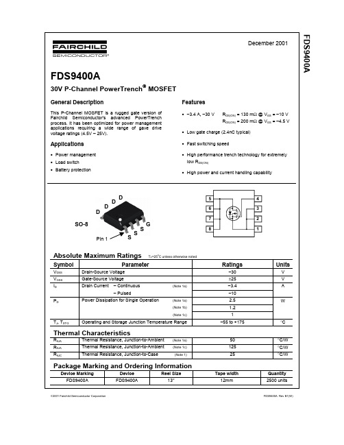
D D SO-8
D D
DD D D
5 6
4 3 2 1
Pin 1 SO-8
G G S S S S S S
TA=25oC unless otherwise noted
7 8
(Note 2)
mV/°C µA NA NA V mV/°C 130 200 210 mΩ
On Characteristics
Gate Threshold Voltage Gate Threshold Voltage Temperature Coefficient Static Drain–Source On–Resistance On–State Drain Current Forward Transconductance Input Capacitance Output Capacitance Reverse Transfer Capacitance
–3
ID(on) gFS Ciss Coss Crss td(on) tr td(off) tf Qg Qgs Qgd IS VSD
A S pF pF pF 9 23 20 4 3.5 ns ns ns ns nC nC nC A V
Dynamic Characteristics
VDS = –15 V, f = 1.0 MHz V GS = 0 V,
(Note 2)
Test Conditions
VGS = 0 V, ID = –250 µA ID = –250 µA, Referenced to 25°C VDS = –24 V, VGS = 25 V, VGS = –25 V, VGS = 0 V VDS = 0 V VDS = 0 V
- 1、下载文档前请自行甄别文档内容的完整性,平台不提供额外的编辑、内容补充、找答案等附加服务。
- 2、"仅部分预览"的文档,不可在线预览部分如存在完整性等问题,可反馈申请退款(可完整预览的文档不适用该条件!)。
- 3、如文档侵犯您的权益,请联系客服反馈,我们会尽快为您处理(人工客服工作时间:9:00-18:30)。
3
V mV/°C Ω
0.028 0.048 0.042
ID(on) gFS
VGS = 10 V, VDS = 10 V,
20 20
A S
Dynamic Characteristics
Ciss Coss Crss Input Capacitance Output Capacitance Reverse Transfer Capacitance
FDS6912 Rev E (W)
元器件交易网
FDS6912
Typical Characteristics (continued)
10 ID = 6.3A 8 15V 6 VDS = 5V 10V2000CAPACITANCE (pF)
1000 500
C iss
4
C oss
200 80
2
f = 1 MHz VGS = 0V
0.1 0.3 1 3 10
C rss
30
0 0 4 8 Qg, GATE CHARGE (nC) 12 16
V DS , DRAIN TO SOURCE VOLTAGE (V)
TA=25 C unless otherwise noted
o
Parameter
Ratings
30 ±25
(Note 1a)
Units
V V A W
6 20 2
Power Dissipation for Dual Operation Power Dissipation for Single Operation
0.8 0 10 20 30 40 50
ID, DRAIN CURRENT (A)
Figure 1. On-Region Characteristics.
Figure 2. On-Resistance Variation with Drain Current and Gate Voltage.
8
1.6 1.5 DRAIN-SOURCE ON-RESISTANCE 1.4 1.3 1.2 1.1 1.0 0.9 0.8
TA = 25°C unless otherwise noted
Parameter
Drain–Source Breakdown Voltage Breakdown Voltage Temperature Coefficient Zero Gate Voltage Drain Current Gate–Body Leakage, Forward Gate–Body Leakage, Reverse
30
VGS = 10V
24 I , DRAIN-SOUR CE CURREN T (A)
6.0V 5.0V 4.5V
2 1.8 1.6 V GS = 4.0V
18
4.0V
12
1.4 1.2 1
4.5V 5.0V
3.5V
6.0V 7.0V 10V
D
6
3.0V
0 0 1 1 2 2 V DS, D RAIN-SOUR CE VOL TAGE (V) 3 3
元器件交易网
FDS6912
July 2000
FDS6912
Dual N-Channel Logic Level PWM Optimized PowerTrench MOSFET
General Description
These N-Channel Logic Level MOSFETs have been designed specifically to improve the overall efficiency of DC/DC converters using either synchronous or conventional switching PWM controllers. These MOSFETs feature faster switching and lower gate charge than other MOSFETs with comparable RDS(ON) specifications. The result is a MOSFET that is easy and safer to drive (even at very high frequencies), and DC/DC power supply designs with higher overall efficiency.
IS VSD Maximum Continuous Drain–Source Diode Forward Current Drain–Source Diode Forward Voltage VGS = 0 V, IS = 1.3 A
(Note 2)
1.3 0.75 1.2
A V
Notes: 1. RθJA is the sum of the junction-to-case and case-to-ambient thermal resistance where the case thermal reference is defined as the solder mounting surface of the drain pins. RθJC is guaranteed by design while RθCA is determined by the user's board design.
a) 78°/W when 2 mounted on a 0.5in pad of 2 oz copper
b) 125°/W when mounted on a 0.02 2 in pad of 2 oz copper
c) 135°/W when mounted on a minimum mounting pad.
2000 Fairchild Semiconductor Corporation
FDS6912 Rev F (W)
元器件交易网
FDS6912
Electrical Characteristics
Symbol
BVDSS ∆BVDSS ∆TJ IDSS IGSSF IGSSR
D1 D1 D2 D2 S1 G1
5 6 7
Q1
4 3 2
Q2
SO-8
S2
8
1
G2
Absolute Maximum Ratings
Symbol
VDSS VGSS ID PD Drain-Source Voltage Gate-Source Voltage Drain Current – Continuous – Pulsed
Scale 1 : 1 on letter size paper 2. Pulse Test: Pulse Width < 300µs, Duty Cycle < 2.0%
FDS6912 Rev E (W)
元器件交易网
FDS6912
Typical Characteristics
100
VDS = 5V
I D , DRAIN CURRENT (A) 15
TJ = -55°C
25°C 125°C
10
VGS = 0V
TA = 125 C 1 25 C
o
o
10
0.1 0.01
-55 C
o
5
0.001 0.0001
0
0 1 2 3 4 V GS , GATE TO SOURCE VOLTAGE (V) 5
(Note 1a) (Note 1)
78 40
°C/W °C/W
Package Marking and Ordering Information
Device Marking FDS6912 Device FDS6912 Reel Size 13’’ Tape width 12mm Quantity 2500 units
1 2 4 V
GS
25 o C
6 ,GATE-SOURCE VOLTAGE (V) 8 10
Figure 3. On-Resistance Variation withTemperature.
20
Figure 4. On-Resistance Variation with Gate-to-Source Voltage.
Features
• 6 A, 30 V. RDS(ON) = 0.028 Ω @ VGS = 10 V RDS(ON) = 0.042 Ω @ VGS = 4.5 V.
• Optimized for use in switching DC/DC converters with PWM controllers • Very fast switching. • Low gate charge
Min
30
Typ
Max Units
V
Off Characteristics
20 1 10 100 –100 mV/°C µA nA nA
On Characteristics
VGS(th) ∆VGS(th) ∆TJ RDS(on)
Gate Threshold Voltage Gate Threshold Voltage Temperature Coefficient Static Drain–Source On–Resistance On–State Drain Current Forward Transconductance
(Note 2)
Test Conditions
VGS = 0 V, ID = 250 µA ID = 250 µA, Referenced to 25°C VDS = 24 V, VGS = 25 V, VGS = –25 V VGS = 0 V TJ = 55°C VDS = 0 V VDS = 0 V