P-5LG_1中文资料
API-5LD中文版
抗腐蚀合金复合钢管或衬管规范API 5LD规范第二版1998年7月生效日期:1998年12月31日特别说明API出版物仅对普遍性问题做出了规定。
对一些特殊情况,应查阅联邦、州和地方的有关法规。
API不为供应商、制造商和雇主承担其雇员在健康、安全风险及预防措施进行教育、培训和装备等方面的义务。
亦不承担他们因违反联邦、州和地方法律而应负的责任。
有关健康、安全风险及预防措施方面的详细资料或情况可向雇主、供应商或制造商索取,或从材料的安全数据表处得到。
API出版物不能以任何方式解释为授予任何人权利不制造、销售或使用属于专利证书所涉及的方法、设备或产品。
同样不能解释为保证任何人因侵犯专利权而不承担责任。
一般情况下,API标准每5年至少进行一次复审、修改、重新确认或予以撤销。
有时审定周期会延长,延长期不超过两年。
所以,除已授权再版延期外,作为现行的API标准自出版之日起,5年后不再有效。
可向API勘探开发部[电话:(202)6828000]了解本出版物情况。
API每年颁布一次出版物和资料目录,每季度订正一次变动情况,API地址位于:American Petroleum Institute,1220,L Street,N.W.Washington,D.C.20005。
本文件是在保证获得适当通知和参与开发工作的基础上,根据API标准化程序制定的,称之为API标准。
涉及到本标准内容的解释和本标准制定程序的问题,请直接致函美国石油学会勘探开发部部长。
地址:American Petroleum Institute,1220,L Street,N.W.Washington,D.C.20005。
要求复制或翻译本资料全文或任一部分也可致函商务部长。
API标准的出版便于已被证实的安全可靠的技术工艺及具体做法的推广应用。
考虑到这些标准的使用时间和地点,这些标准无意排除对采用可靠技术方法的需求。
API标准的制定和出版无意以任何方式禁止任何人采用其它标准。
P-5LG资料

•Ÿ
Specification (P-5LG/SW) (Part No. S1325005)
Item Inductance Unloaded Q Using Frequency: 4MHz 5 ƒÊ (1-4) H ± 4% Variable Measuring Condition 7.96MHz 7.96MHz
•Ÿ
Dimensions (mm)
.}.2 2 0• 8
.1 0{•
.0 6
..5 1 0 |• 0 .4 0
..5 0 Ó ƒ 40 | • 0
.1 0 {•
.5•.5 3 0} 1
(Color:Wite) h
.5 6
MAX .
..4 2 }• 0 6
.5•.5 3 0} 1 5.8}.3 0•
•– •– •– •Ÿ
Dimension does not include solder used on coil. Pin pitch shall be measured at the root of terminal. Dimension without tolerance are approx.
Connection (Bottom View)
元器件交易网
IFT COILS < Pin Type: P-5 Series>
Type: P-5LG/FM, P-5LG/AM, P-5LG/MW, P-5LG/SW
Product Description
•Ÿ
•E 6.0×5.9mm Max.(L×W), 6.5mm Max. Height. •E Inductance:1~680µH Max. •E Operating frequency:20MHz Max. •E In addition to the reference versions of parameters shown here,custom designs are available to meet your exact requirements.
LDP-5完整介绍

IEC-270 Standard Circuit Connections
B
C LDM-5
D
A
LDP-5
A - Differential LEMKE probe LDP-5 B - Coupling capacitor C - Measuring impedance LDM-5 D - Connection cable
完整的爱剧情介绍tcpip完整基础介绍海贼王成员完整介绍终结者5高清完整版玉蒲团5完整版高清上位完整版剧情介绍妈咪电影完整版介绍速度与激情5完整版虎胆威龙5完整版supershow5完整版
On-Line Partial Discharge Measurement on Power Transformers
Very accurate (Pinpointing in less than 1/2 inch)
Requires direct access to the insulator surface Does not work through shields Safety distances to HV electrodes can prevent the use
Using the Noise Filter LDF-5
AM Radio
A - Sensor with PD + AM signal B - Band-Stop Filter LDF-5 C - Signal without AM Noise D - Differential LEMKE probe LDP-5
LDP-5 in Differential Mode
Differential Mode
LDP-5
A
A - PD site in the insulation (not shielded, e.g. Bushings) B - Differential LEMKE probe LDP-5 with two small C-sensors at the differential inputs
PI5101-EVAL1;PI5101-00-LGIZ;中文规格书,Datasheet资料

Maximum Rating and Thermal Characteristics (TA = 25°C unless otherwise Specified)
Parameter Drain-to-Source Voltage Gate-to-Source Voltage Drain Current Single Pulse Avalanche Current Maximum Power Dissipation Operating Junction and Storage Temperature Range Thermal Resistance
PI5101
μRDS(on) FETTM Series
360μΩ, 5V/60A N-Channel MOSFET
Product Summary
Condition TA = 25°C ID = 5mA VGS = 4.5V VGS = 3.5V VGS = 4.5V 60ADC 5V 360μΩ 380μΩ 65nC 0.1Ω 0.1nH Value Max Min Typ Typ Typ Typ Typ
VGS = 1.0V
0.2
0.4
0.6
0.8
0 0.5
0.6
0.7
0.8
0.9
1.0
1.1
1.2
VDS - Drain-to-Source Voltage [V]
VGS - Gate-to-Source [V]
Figure 1: Output Characteristics. (Pulsed VGS)
Picor Corporation •
PI5101-00-LGIZ
Rev 1.0, Jan 25th 2010
1956551资料
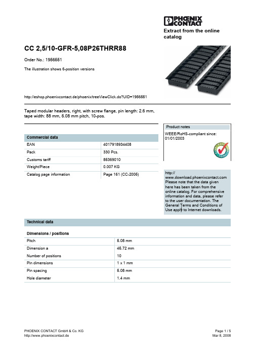
Extract from the onlinecatalogCC 2,5/10-GFR-5,08P26THRR88Order No.: 1956551The illustration shows 6-position versionshttp://eshop.phoenixcontact.de/phoenix/treeViewClick.do?UID=1956551Taped modular headers, right, with screw flange, pin length: 2.6 mm, tape width: 88 mm, 5.08 mm pitch, 10-pos.http://Please note that the data givenhere has been taken from theonline catalog. For comprehensiveinformation and data, please referto the user documentation. TheGeneral Terms and Conditions ofUse apply to Internet downloads. Technical dataDimensions / positionsPitch 5.08 mmDimension a45.72 mmNumber of positions10Pin dimensions 1 x 1 mmPin spacing 5.08 mmHole diameter 1.4 mmTechnical dataInsulating material group IIIaRated surge voltage (III/3) 4 kVRated surge voltage (III/2) 4 kVRated surge voltage (II/2) 4 kVRated voltage (III/2)320 VRated voltage (II/2)400 VConnection in acc. with standard EN-VDENominal current I N12 ANominal voltage U N250 VMaximum load current12 A (per position)Insulating material LCPInflammability class acc. to UL 94V0Certificates / ApprovalsApproval logoCULNominal voltage U N300 VNominal current I N10 AULNominal voltage U N300 VNominal current I N10 ACertification CUL, ULAccessoriesItem Designation DescriptionGeneral1954362CR-MSTB NAT HT HT coding section, is pushed into the recess on the header beforethe reflow process, made of highly temperature-resistant, beigeinsulating materialMarking1051993B-STIFT Marker pen, for manual labeling of unprinted Zack strips, smear-proof and waterproof, line thickness 0.5 mm0804293SK 5,08/3,8:FORTL.ZAHLEN Marker card, printed horizontally, self-adhesive, 12 identicaldecades marked 1-10, 11-20 etc. up to 91-(99)100, sufficient for120 terminal blocks0805085SK 5,08/3,8:SO Marker card, special printing, self-adhesive, labeled acc. tocustomer requirements, 12 identical marker strips per card, max.25-position labeling per strip, color: white0805412SK 5,08/3,8:UNBEDRUCKT Marker cards, unprinted, with pitch divisions, self-adhesive, 10-section marker strips, 12 strips per card, can be labeled with theM-PENPlug/Adapter1734401CR-MSTB Coding section, inserted into the recess in the header or theinverted plug, red insulating materialDrawingsApplication drawingDrilling diagramDimensioned drawingBottom view, free space for solder paste, 0.5mm deepDirection of the arrow = feeding directionAddressPHOENIX CONTACT GmbH & Co. KGFlachsmarktstr. 832825 Blomberg,GermanyPhone +49 5235 3 00Fax +49 5235 3 41200http://www.phoenixcontact.de© 2008 Phoenix ContactTechnical modifications reserved;。
PQ05RF1_01中文资料

Unit
V
% % %/˚C dB V V µA V mA mA
V
❇3 PQ05RF1 series:VIN=7V, PQ09RF1 seris:VIN=15V, PQ12RF1 seris:VIN=18V ❇4 PQ05RF1/PQ05RF11/PQ05RF1V:VIN=6 to 12V
OFF-state current for control PQ05RF1/PQ05RF11 series
Quiescent current
Output voltage minute adjustment characteristics
PQ05RF1V PQ09RF1V PQ12RF1V
Symbol
Overheat protection circuit
3 •Please refer to the chapter " Handling Precautions ".
Notice In the absence of confirmation by device specification sheets,SHARP takes no responsibility for any defects that may occur in equipment using any SHARP devices shown in catalogs,data books,etc.Contact SHARP in order to obtain the latest device specification sheets before using any SHARP device.
元器件Lo交w P易o网wewr-wLwos.cseVcbo2ltba.gcoemRegulators
PMEG2005AEL,315;中文规格书,Datasheet资料

1.Product profile1.1General descriptionPlanar Maximum Efficiency General Application (MEGA) Schottky barrier diode with an integrated guard ring for stress protection encapsulated in a SOD882 leadless ultra small plastic package.1.2FeaturesForward current: 0.5AReverse voltage: 20V Ultra low forward voltageLeadless ultra small plastic packagePower dissipation comparable to SOT231.3ApplicationsUltra high-speed switching Voltage clamping Protection circuitsLow voltage rectificationHigh efficiency DC-to-DC conversionLow power consumption applications1.4Quick reference dataPMEG2005AEL0.5A ultra low V F MEGA Schottky barrier rectifier in leadless ultra small SOD882 packageRev. 03 — 15 January 2010Product data sheetTable 1.Quick reference dataSymbol Parameter Value Unit I F forward current 0.5A V Rreverse voltage20V2.Pinning information[1]The marking bar indicates the cathode.3.Ordering information4.Marking5.Limiting valuesTable 2.Discrete pinningPin Description Simplified outline Symbol1cathode [1]2anode001aaa332Bottom viewTop view21sym00112Table 3.Ordering informationType number Package NameDescriptionVersion PMEG2005AEL-leadless ultra small plastic package; 2 terminals; body 1.0×0.6×0.5mmSOD882Table 4.MarkingType number Marking code PMEG2005AELF2Table 5.Limiting valuesIn accordance with the Absolute Maximum Rating System (IEC 60134).Symbol Parameter Conditions Min Max Unit V R continuous reverse voltage -20V I F continuous forward current-0.5A I FRM repetitive peak forward current t p ≤1ms; δ≤0.25- 2.5A I FSM non-repetitive peak forward currentt =8ms square wave-3A T j junction temperature[1]-150°C T amb operating ambient temperature [1]−65+150°C T stgstorage temperature−65+150°C[1]For Schottky barrier diodes thermal run-away has to be considered, as in some applications the reverse power losses P R are a significant part of the total power losses. Nomograms for determining the reverse power losses P R and I F(AV) rating will be available on request.6.Thermal characteristics[1]Refer to SOD882 standard mounting conditions (footprint), FR4 with 60μm copper strip line.[2]For Schottky barrier diodes thermal run-away has to be considered, as in some applications the reverse power losses P R are a significant part of the total power losses. Nomograms for determining the reverse power losses P R and I F(AV) rating will be available on request.7.Characteristics[1]Pulse test: t p ≤300μs; δ≤0.02.Table 6.Thermal characteristics Symbol ParameterConditions Value Unit R th(j-a)thermal resistance from junction to ambientin free air[1][2]500K/WTable 7.CharacteristicsT amb =25°C unless otherwise specified.Symbol Parameter Conditions Typ Max Unit V Fcontinuous forward voltagesee Figure 1;I F =0.1mA 2560mV I F =1mA 75110mV I F =10mA 135190mV I F =100mA 220290mV I F =500mA375440mV I Rcontinuous reverse currentsee Figure 2;[1]V R =10V 210600μA V R =20V3701500μA C ddiode capacitanceV R =1V; f =1MHz; see Figure 31925pF8.Package outlineLeadless ultra small plastic package; 2 terminals; body 1.0 x 0.6 x 0.5 mm SOD882Fig 4.Package outline9.Revision historyTable 8.Revision historyDocument ID Release date Data sheet status Change notice SupersedesPMEG2005AEL_320100115Product data-PMEG2005AEL_2 Modifications:•This data sheet was changed to reflect the new company name NXP Semiconductors,including new legal definitions and disclaimers. No changes were made to the technicalcontent.PMEG2005AEL_220040427Product data-PMEG2005AEL_1 PMEG2005AEL_120040419Product data--10.Legal information10.1Data sheet status[1]Please consult the most recently issued document before initiating or completing a design. [2]The term ‘short data sheet’ is explained in section “Definitions”.[3]The product status of device(s) described in this document may have changed since this document was published and may differ in case of multiple devices. The latest product status information is available on the Internet at URL .10.2DefinitionsDraft — The document is a draft version only. The content is still under internal review and subject to formal approval, which may result in modifications or additions. NXP Semiconductors does not give any representations or warranties as to the accuracy or completeness ofinformation included herein and shall have no liability for the consequences of use of such information.Short data sheet — A short data sheet is an extract from a full data sheet with the same product type number(s) and title. A short data sheet is intended for quick reference only and should not be relied upon to contain detailed and full information. For detailed and full information see the relevant full data sheet, which is available on request via the local NXP Semiconductors sales office. In case of any inconsistency or conflict with the short data sheet, the full data sheet shall prevail.10.3DisclaimersGeneral — Information in this document is believed to be accurate andreliable. However, NXP Semiconductors does not give any representations or warranties, expressed or implied, as to the accuracy or completeness of such information and shall have no liability for the consequences of use of such information.Right to make changes — NXP Semiconductors reserves the right to make changes to information published in this document, including withoutlimitation specifications and product descriptions, at any time and without notice. This document supersedes and replaces all information supplied prior to the publication hereof.Suitability for use — NXP Semiconductors products are not designed, authorized or warranted to be suitable for use in medical, military, aircraft, space or life support equipment, nor in applications where failure ormalfunction of an NXP Semiconductors product can reasonably be expected to result in personal injury, death or severe property or environmentaldamage. NXP Semiconductors accepts no liability for inclusion and/or use of NXP Semiconductors products in such equipment or applications and therefore such inclusion and/or use is at the customer’s own risk.Applications — Applications that are described herein for any of these products are for illustrative purposes only. NXP Semiconductors makes no representation or warranty that such applications will be suitable for the specified use without further testing or modification.Limiting values — Stress above one or more limiting values (as defined in the Absolute Maximum Ratings System of IEC 60134) may cause permanent damage to the device. Limiting values are stress ratings only and operation of the device at these or any other conditions above those given in theCharacteristics sections of this document is not implied. Exposure to limiting values for extended periods may affect device reliability.Terms and conditions of sale — NXP Semiconductors products are sold subject to the general terms and conditions of commercial sale, as published at /profile/terms , including those pertaining to warranty, intellectual property rights infringement and limitation of liability, unlessexplicitly otherwise agreed to in writing by NXP Semiconductors. In case of any inconsistency or conflict between information in this document and such terms and conditions, the latter will prevail.No offer to sell or license — Nothing in this document may be interpreted or construed as an offer to sell products that is open for acceptance or the grant, conveyance or implication of any license under any copyrights, patents or other industrial or intellectual property rights.Export control — This document as well as the item(s) described herein may be subject to export control regulations. Export might require a prior authorization from national authorities.Quick reference data — The Quick reference data is an extract of theproduct data given in the Limiting values and Characteristics sections of this document, and as such is not complete, exhaustive or legally binding.10.4TrademarksNotice: All referenced brands, product names, service names and trademarks are the property of their respective owners.11.Contact informationFor more information, please visit: For sales office addresses, please send an email to: salesaddresses@Document status [1][2]Product status [3]DefinitionObjective [short] data sheet Development This document contains data from the objective specification for product development. Preliminary [short] data sheet Qualification This document contains data from the preliminary specification. Product [short] data sheetProductionThis document contains the product specification.12.Contents1Product profile. . . . . . . . . . . . . . . . . . . . . . . . . . 11.1General description . . . . . . . . . . . . . . . . . . . . . 11.2Features. . . . . . . . . . . . . . . . . . . . . . . . . . . . . . 11.3Applications . . . . . . . . . . . . . . . . . . . . . . . . . . . 11.4Quick reference data . . . . . . . . . . . . . . . . . . . . 12Pinning information. . . . . . . . . . . . . . . . . . . . . . 23Ordering information. . . . . . . . . . . . . . . . . . . . . 24Marking. . . . . . . . . . . . . . . . . . . . . . . . . . . . . . . . 25Limiting values. . . . . . . . . . . . . . . . . . . . . . . . . . 26Thermal characteristics . . . . . . . . . . . . . . . . . . 37Characteristics. . . . . . . . . . . . . . . . . . . . . . . . . . 38Package outline. . . . . . . . . . . . . . . . . . . . . . . . . 59Revision history. . . . . . . . . . . . . . . . . . . . . . . . . 610Legal information. . . . . . . . . . . . . . . . . . . . . . . . 710.1Data sheet status . . . . . . . . . . . . . . . . . . . . . . . 710.2Definitions. . . . . . . . . . . . . . . . . . . . . . . . . . . . . 710.3Disclaimers. . . . . . . . . . . . . . . . . . . . . . . . . . . . 710.4Trademarks. . . . . . . . . . . . . . . . . . . . . . . . . . . . 711Contact information. . . . . . . . . . . . . . . . . . . . . . 712Contents. . . . . . . . . . . . . . . . . . . . . . . . . . . . . . . 8Please be aware that important notices concerning this document and the product(s)described herein, have been included in section ‘Legal information’.© NXP B.V.2010.All rights reserved.For more information, please visit: For sales office addresses, please send an email to: salesaddresses@分销商库存信息: NXPPMEG2005AEL,315。
P-G-1-G-1资料

FEATURES•Economical miniature high-density connectors suitable for high-reliability and military applications.•0.100" (2.54mm) square grid rack and panel connectors with male and female insulators are available in four sizes:33, 75, 117 and 165 contacts.•Insertable / removable mini-varilok and mini-wrap contacts.•Crimp and/or solderless wrap terminations.•E xceptional versatility: all hardware can be mounted on plug or receptacle (see ordering code).•Actuating screw facilitates mating and unmating; locks mated connectors together.•Keyed and shrouded insulator design prevents incorrect mating and protects contacts from mishandling.•Simplified polarizing hardware permits 36 polarization combinations per connector pair.•Optional covers with top or side cable entry and clamp.•Optional cable clamps.•Choice of any combination of hardware — or no hardware.•U.L. recognized-diallyl phthalate material.Current Rating:5 amperesContact Resistance:6 milliohmsWithdrawal Force:2 to 8 ounces max. per contact Material:Phosphor BronzeStandard Plating:Gold, 10 microinches min., over Nickel,50-100 microinches Spacing:0.100" (2.54mm)TECHNICAL SPECIFICATIONS CONTACTSINSULATORSInsulation Resistance:5,000 megohms, min. (diallyl phthalate insulators)5,000 megohms, min. (polycarbonate insulators)Operating Temperature:-40ºC to +120ºCDielectric Withstanding Voltage:Sea Level: 1,000 Volts rms Materials:0.100" (2.54mm) spacing – diallyl phthalate, glass-filled, flame resistantORDERING CODE008026033Number of Contacts 033 = 33075 = 75 117 = 117165 = 165000Contact CodeOrder crimp contactsseparately by Part Number.Otherwise specify contact code 491.000 = Crimp (3000 - contact reel)Part Number 60 8216 0323 00 339000 = Crimp (loose contact)Accepts #22-30 AWG wirePart Number 60 8216 0313 00 339491 = Wire wrappable removable contact .025"(.635mm) sq. x .564" (14.33mm) tailPart Number 60 8216 0413 00 339803Variation CodeAdd 050 to order alternative keying (Pin & Socket)i.e. 701 = Standard hermaphroditickeying751 = Pin and socket keyingComplete a 15 digit assembly number for each mating part, male and female.VARIATION CODESVariation Code No.Insulator Cover Cover Cable Actuating FixedKeying Body Without Small Large EntranceNut Screw Hardware TypeCover Clamp Clamp501——No Yes No Yes 502——No Yes No No 503——No No Yes Yes 504——No No Yes No —505513Top Yes No Yes —506514Side Yes No Yes Male—507515Top Yes No No (Exposed —508516Side Yes No No Contacts)—509517Top No Yes Yes —510518Side No Yes Yes —511519Top No Yes No —512520Side No Yes No 601——No No Yes Yes 602——No No Yes No 603——No Yes No Yes 604——No Yes No No —605613Top No Yes Yes —606614Side No Yes Yes Female —607615Top No Yes No (Recessed —608616Side No Yes No Contacts)—609617Top Yes No Yes —610618Side Yes No Yes —611619Top Yes No No —612620Side Yes No NoT able 4Varicon ®Series 8026 – 0.100" Rectangular Connector33 CONTACTSFemale Plug (Recessed Contacts)For variation code number See Table 1See Table 2Page 29Page 2975 CONTACTSFemale Plug (Recessed Contacts)For variation code number See Table 3See Table 4Page 29Page 29EE E E E E E ESERIES 8026 COVER CROSS REFERENCE. FOR DETAILS SEE PAGE 21Varicon®Series 8026 – 0.100" Rectangular ConnectorPOLARIZATION / KEYING ALTERNATIVE KEYINGEXAMPLE (PIN & SOCKET)PInsulator Body TypeP = Male, R = FemaleLSLeft Side Pin5Left Side Pin Position1 through 6RSRight Side Pin Right Side Pin Position1 through 6NOTE:Same size of pin and socket keying hardware are usedon all existing 8026 connectors (33, 75, 117, 165) – both sides POLARIZATION CODEPolarizing pins, when desired, are factory set in position #1.Customer can reset as shown below, use tool No. 06 198902. To order factory settings other than position #1, fill outthe “Polarizing Code” below and submit it along with thecompleted connector ordering code.。
- 1、下载文档前请自行甄别文档内容的完整性,平台不提供额外的编辑、内容补充、找答案等附加服务。
- 2、"仅部分预览"的文档,不可在线预览部分如存在完整性等问题,可反馈申请退款(可完整预览的文档不适用该条件!)。
- 3、如文档侵犯您的权益,请联系客服反馈,我们会尽快为您处理(人工客服工作时间:9:00-18:30)。
•Ÿ
Connection (Bottom View)
‡B ‡C
S
‡B
‡C
S
S ‡B ‡A ‡@
‡C
S
‡B ‡A
‡C
‡A
‡A
‡E
S ‡@
S ‡@
P-5LG/MW
‡E
‡E
S ‡@
‡E
P-5LG/AM “S” is winding start
P-5LG/SW
P-5LG/FM
Please refer to the sales offices on our website for a representative near you
•E •E •E
•E Inductance:1~680ƒÊ
In addition to the reference versions of parameters shown here,custom designs are available to meet your exact requirements.
•Ÿ
Feature
•E •E •E •E
•Ÿ
Variable shielded high Q types. AM,MW,SW,FM types are all available. Internally assembled condenser is available. RoHS Compliance
Variable
‚P‚O .‚V MHz
Please refer to the sales offices on our website for a representative near you
2/2
•Ÿ
Specification(P-5LG/MW)
Item Inductance Unloaded Q •i‚P•|‚R•j ‚R‚U‚O µH ±‚S•“ Variable ‚U‚O Min•D Measuring Condition ‚V‚XU‚‹ ‚V‚XU‚‹ H‚š H‚š
•Ÿ
Specification(P-5LG/SW)
Item Frequency Capacity (Int.) Unloaded Q ‚S‚T‚T‚‹ •i‚P•|‚R•j H‚š ±‚Q•“ Variable ‚S‚T‚T‚‹ H‚š Measuring Condition
‚P‚W‚O‚•e ±‚P‚O•“ ‚U‚O ±‚Q‚O•“ Within
5.8•0.3 }
0.4
Dimension (mm)
1/2
元器件交易网
IFT COILS < Pin Type P-5 Series>
Type: P-5LG/AM, P-5LG/MW, P-5LG/SW , P-5LG/FM
•Ÿ
Specification(P-5LG/AM)
元器件交易网
IFT COILS < Pin Type P-5 Series>
Type: P-5LG/AM, P-5LG/MW, P-5LG/SW , P-5LG/FM
•Ÿ
Product Description
6.1×6.1mm Max.(L×W), 6.5mm Max. Height. H Max. Operating frequency:20MHz Max.
Item Inductance Unloaded Q ‚P‚P‚T •i‚S•|‚U•j µ‚g ±‚T•“ ‚T‚O Min•D Variable
Measuring Condition
‚V‚XU‚‹ ‚V‚XU‚‹
H‚š H‚š
Hale Waihona Puke •ŸSpecification(P-5LG/FM)
Item Frequency Unloaded Q Capacity (INT.) •i‚P•|‚R•j ‚P‚O .‚V MHz±‚Q•“ ‚T‚T Min•D ‚T‚P‚•e ±‚P‚O•“ Measuring Condition
2.8•0.2 }
0.1 {• 0.40.05 Óƒ |•
6.0
0.1 {• 1.0•0.05 |
.5•0.15 3 }
(Color:White)
6.5 MAX .
2.6•0.4 }
.5•0.15 3 } 5.8•0.3 }
•– •– •–
Dimension does not include solder used on coil. Pin pitch shall be measured at the root of terminal. Dimension without tolerance are approx.