MAX6314US28D4中文资料
MAX4614中文资料
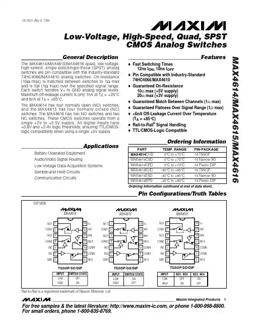
Ordering Information
PART
TEMP. RANGE PIN-PACKAGE
MAX4614CUD
0°C to +70°C
14 TSSOP
MAX4614CSD
0°C to +70PD
0°C to +70°C
V+ = 5.5V; VCOM_ = 1V, 4.5V; VNO_ = VNC_= 1V, 4.5V, or floating
TSSOP/SO/DIP
INPUT LOW HIGH
SWITCH STATE OFF ON
TSSOP/SO/DIP
INPUT
LOW HIGH
SWITCH STATE
ON OFF
TSSOP/SO/DIP
INPUT LOW HIGH
NO1, NO3 OFF ON
NC2, NC4 ON OFF
Rail-to-Rail is a registered trademark of Nippon Motorola, Ltd.
14 Plastic DIP
MAX4614EUD -40°C to +85°C
14 TSSOP
MAX4614ESD
-40°C to +85°C
14 Narrow SO
MAX4614EPD
-40°C to +85°C
14 Plastic DIP
Ordering Information continued at end of data sheet.
元器件交易网
19-1501; Rev 0; 7/99
MAX4614/MAX4615/MAX4616
DS_AW6314_CN_V1.1_IIC接口_双输入_四通道SIM卡接口控制器
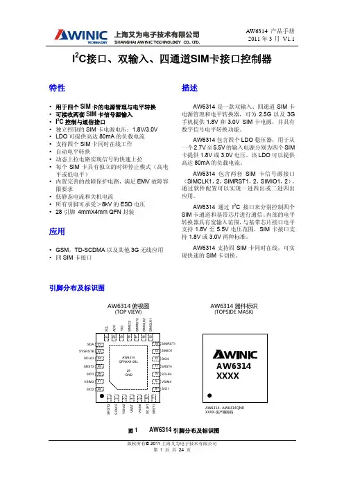
I 2C 接口、双输入、四通道SIM 卡接口控制器特性y 用于四个SIM 卡的电源管理与电平转换 y 可接收两套SIM 卡信号源输入 y I 2C 控制与通信接口y 独立控制的SIM 卡电源电压:1.8V/3.0V y LDO 可提供高达80mA 的负载电流 y 支持四个SIM 卡同时在线工作 y 自动电平转换y 动态上拉电路实现信号的快速上拉y 每个SIM 卡具有独立的时钟停止模式(高电平或低电平)y 内置完善的故障保护电路,满足EMV 故障容限要求y 低静态电流和关机电流y 所有引脚可承受>8kV 的ESD 电压 y 28引脚 4mmX4mm QFN 封装应用y GSM ,TD-SCDMA 以及其他3G 无线应用 y 四SIM 卡接口描述AW6314是一款双输入、四通道SIM 卡电源管理和电平转换器,可为2.5G 以及3G 手机提供1.8V 和3.0V SIM 卡电源,并具有数字信号电平转换功能。
AW6314包含四个LDO 稳压器,用于从一个2.7V 至5.5V 的输入电源分别为四个SIM 卡提供1.8V 或3.0V 电压。
该LDO 可以提供高达80mA 的负载电流。
AW6314包含两套SIM 卡信号源接口(SIMCLK1,2,SIMRST1,2,SIMIO1,2),通过软件配置可以实现一进四出或二进四出应用。
AW6314通过I 2C 接口来分别控制四个SIM 卡通道和基带芯片进行通信。
内部的电平转换器具有宽输入范围,与基带芯片接口电平支持1.8V 至5.5V 电压范围,SIM 卡接口支持1.8V 或3.0V 两种标准。
AW6314支持四SIM 卡同时在线,可实现快速的SIM 卡切换。
引脚分布及标识图AW6314- AW6314QNR XXXX-生产跟踪码AW6314 器件标识(TOPSIDE MASK)AW6314 俯视图(TOP VIEW)V S I M 2V I OV B A TA D 0C LSRST3SIO3S C L K 2S R S T 2SIO2VSIM3SCLK3S R S T 1SIO1SIMIO1SIMRST1I M C L K 1VSIM4SCLK4SIO4SRST4V S I M 1S C L K 1SDA SYSRSTB I M I O 2I M R S T 2I M C L K 2图 1 AW6314引脚分布及标识图典型应用图注1:在I2C总线SDA、SCL上预留30pF电容(靠近AW6314),有利于增强接口的抗干扰能力。
MAX6348XR中文资料
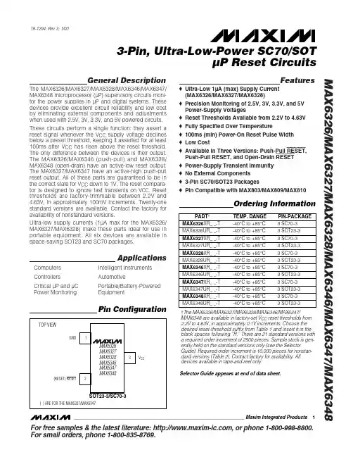
For free samples & the latest literature: , or phone 1-800-998-8800.For small orders, phone 1-800-835-8769.General DescriptionThe MAX6326/MAX6327/MAX6328/MAX6346/MAX6347/MAX6348 microprocessor (µP) supervisory circuits moni-tor the power supplies in µP and digital systems. These devices provide excellent circuit reliability and low cost by eliminating external components and adjustments when used with 2.5V, 3V, 3.3V, and 5V powered circuits.These circuits perform a single function: they assert a reset signal whenever the V CC supply voltage declines below a preset threshold, keeping it asserted for at least 100ms after V CC has risen above the reset threshold.The only difference between the devices is their output.The MAX6326/MAX6346 (push-pull) and MAX6328/MAX6348 (open-drain) have an active-low reset output.The MAX6327/MAX6347 have an active-high push-pull reset output. All of these parts are guaranteed to be in the correct state for V CC down to 1V. The reset compara-tor is designed to ignore fast transients on V CC . Reset thresholds are factory-trimmable between 2.2V and 4.63V, in approximately 100mV increments. Twenty-one standard versions are available. Contact the factory for availability of nonstandard versions.Ultra-low supply currents (1µA max for the MAX6326/MAX6327/MAX6328) make these parts ideal for use in portable equipment. All six devices are available in space-saving SOT23 and SC70 packages.ApplicationsComputers Intelligent Instruments Controllers AutomotiveCritical µP and µC Portable/Battery-Powered Power MonitoringEquipmentFeatureso Ultra-Low 1µA (max) Supply Current (MAX6326/MAX6327/MAX6328)o Precision Monitoring of 2.5V, 3V, 3.3V, and 5V Power-Supply Voltageso Reset Thresholds Available from 2.2V to 4.63V o Fully Specified Over Temperatureo 100ms (min) Power-On Reset Pulse Width o Low Costo Available in Three Versions: Push-Pull RESET ,Push-Pull RESET, and Open-Drain RESET o Power-Supply Transient Immunity o No External Componentso 3-Pin SC70/SOT23 Packageso Pin Compatible with MAX803/MAX809/MAX810MAX6326/MAX6327/MAX6328/MAX6346/MAX6347/MAX63483-Pin, Ultra-Low-Power SC70/SOTµP Reset Circuits________________________________________________________________Maxim Integrated Products 1Pin Configuration19-1294; Rev 3; 1/00†The MAX6326/MAX6327/MAX6328/MAX6346/MAX6347/MAX6348 are available in factory-set V CC reset thresholds from 2.2V to 4.63V, in approximately 0.1V increments. Choose the desired reset-threshold suffix from Table 1 and insert it in the blank spaces following “R.”There are 21 standard versions witha required order increment of 2500 pieces. Sample stock is gen-erally held on the standard versions only (see the SelectorGuide). Required order increment is 10,000 pieces for nonstan-dard versions (Table 2). Contact factory for availability. All devices available in tape-and-reel only.Selector Guide appears at end of data sheet.M A X 6326/M A X 6327/M A X 6328/M A X 6346/M A X 6347/M A X 63483-Pin, Ultra-Low-Power SC70/SOT µP Reset Circuits 2_______________________________________________________________________________________ABSOLUTE MAXIMUM RATINGSELECTRICAL CHARACTERISTICS(V CC = full range, T A = -40°C to +85°C, unless otherwise noted. Typical values are at T A = +25°C and V CC = 3V.) (Note 1)Stresses beyond those listed under “Absolute Maximum Ratings” may cause permanent damage to the device. These are stress ratings only, and functional operation of the device at these or any other conditions beyond those indicated in the operational sections of the specifications is not implied. Exposure to absolute maximum rating conditions for extended periods may affect device reliability.Terminal Voltage (with respect to GND)V CC ...........................................................................-0.3V to +6V RESET, RESET (push-pull).........................-0.3V to (V CC + 0.3V)RESET (open drain)..................................................-0.3V to +6V Input Current (V CC ).............................................................20mA Output Current (RESET, RESET ).........................................20mA Rate of Rise (V CC )...........................................................100V/µsContinuous Power Dissipation (T A = +70°C)3-Pin SC70 (derate 2.7mW/°C above +70°C)...............174mW 3-Pin SOT23 (derate 4mW/°C above +70°C)................320mW Operating Temperature Range ...........................-40°C to +85°C Storage Temperature Range.............................-65°C to +150°C Lead Temperature (soldering, 10s).................................+300°CNote 1:Overtemperature limits are guaranteed by design and not production tested.MAX6326/MAX6327/MAX6328/MAX6346/MAX6347/MAX63483-Pin, Ultra-Low-Power SC70/SOTµP Reset Circuits_______________________________________________________________________________________3__________________________________________Typical Operating Characteristics(T A = +25°C, unless otherwise noted.)00.30.20.10.40.50.60.70.80.91.0-400-2020406080SUPPLY CURRENT vs. TEMPERATURE TEMPERATURE (°C)S U P P L Y C U R R E N T(µA)050100150200-400-2020406080POWER-DOWN RESET DELAY vs. TEMPERATURE TEMPERATURE (°C)R E S E T D E L A Y(µs)130150140160170180190200210-400-2020406080POWER-UP RESET TIMEOUT vs. TEMPERATURE M A X6326-03TEMPERATURE (°C)P O W E R-U P R E S E T T I M E O U T(m s)500011001000MAXIMUM TRANSIENT DURATION vs. RESET THRESHOLD OVERDRIVE (SC70)100300400200M A X6326-04RESET THRESHOLD OVERDRIVE,V TH - V CC (mV)M A X I M U M T R A N S I E N T D U R A T I O N(µs)10______________________________________________________________Pin DescriptionM A X 6326/M A X 6327/M A X 6328/M A X 6346/M A X 6347/M A X 63483-Pin, Ultra-Low-Power SC70/SOT µP Reset Circuits 4___________________________________________________________________________________________________Applications InformationInterfacing to µPs with Bidirectional Reset PinsSince the RESET output on the MAX6328/MAX6348 is open drain, these devices interface easily with micro-processors (µPs) that have bidirectional reset pins,such as the Motorola 68HC11. Connecting the µP supervisor’s RESET output directly to the microcon-troller’s (µC’s) RESET pin with a single pull-up resistor allows either device to assert reset (Figure 1).Negative-Going V CC TransientsIn addition to issuing a reset to the µP during power-up,power-down, and brownout conditions, these devices are relatively immune to short-duration, negative-going V CC transients (glitches).The Typical Operating Characteristics show the Maxi-mum Transient Duration vs. Reset Threshold Overdrive graph, for which reset pulses are not generated. The graph shows the maximum pulse width that a negative-going V CC transient may typically have when issuing a reset signal. As the amplitude of the transient increas-es, the maximum allowable pulse width decreases.Figure 1. Interfacing to µPs with Bidirectional Reset PinsTable 1. Factory-Trimmed Reset Thresholds ‡‡Factory-trimmed reset thresholds are available in approximately 100mV increments with a 1.5% room-temperature variance.MAX6326/MAX6327/MAX6328/MAX6346/MAX6347/MAX63483-Pin, Ultra-Low-Power SC70/SOTµP Reset Circuits_______________________________________________________________________________________5Table 1. Factory-Trimmed Reset Thresholds‡(continued)‡Factory-trimmed reset thresholds are available in approximately 100mV increments with a 1.5% room-temperature variance.Table 2. Device Marking Codes and Minimum Order IncrementsM A X 6326/M A X 6327/M A X 6328/M A X 6346/M A X 6347/M A X 63483-Pin, Ultra-Low-Power SC70/SOT µP Reset Circuits 6__________________________________________________________________________________________________________Chip InformationTRANSISTOR COUNT: 419Table 2. Device Marking Codes and Minimum Order Increments (continued)Selector Guide(standard versions*)*Sample stock is generally held on all standard versions.________________________________________________________Package InformationMAX6326/MAX6327/MAX6328/MAX6346/MAX6347/MAX63483-Pin, Ultra-Low-Power SC70/SOTµP Reset Circuits_______________________________________________________________________________________7M A X 6326/M A X 6327/M A X 6328/M A X 6346/M A X 6347/M A X 63483-Pin, Ultra-Low-Power SC70/SOT µP Reset Circuits Maxim cannot assume responsibility for use of any circuitry other than circuitry entirely embodied in a Maxim product. No circuit patent licenses are implied. Maxim reserves the right to change the circuitry and specifications without notice at any time.8_____________________Maxim Integrated Products, 120 San Gabriel Drive, Sunnyvale, CA 94086 408-737-7600©2000 Maxim Integrated ProductsPrinted USAis a registered trademark of Maxim Integrated Products.Package Information (continued)。
MAX4234中文资料
PARAMETER
SYMBOL
CONDITIONS
MIN
Operating Supply Voltage Range
VDD
Inferred from PSRR test
2.7
Input Offset Voltage
VOS
Input Bias Current
IB
VCM = VSS to VDD
Input Offset Current
DC ELECTRICAL CHARACTERISTICS
(VDD = 2.7V, VSS = 0V, VCM = VDD/2, VOUT = (VDD/2), RL = ∞ connected to (VDD/2), VSHDN = VDD, TA = +25°C, unless otherwise noted.) (Note 2)
MAX6304ESA中文资料
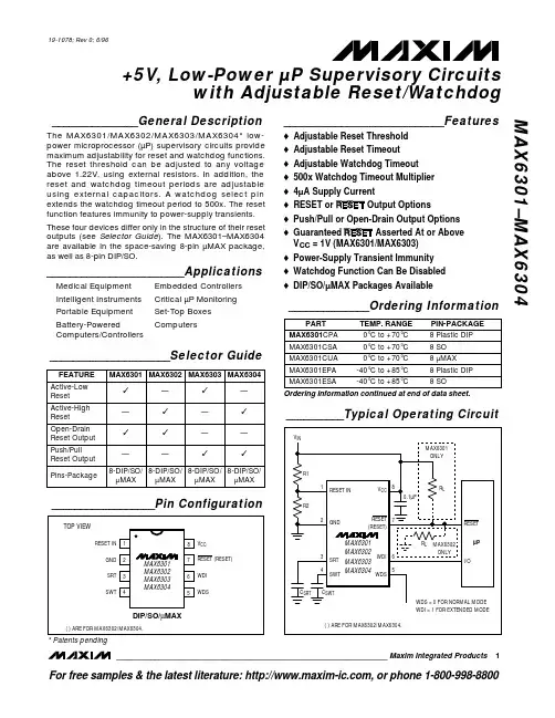
19-1078; Rev 0; 6/96
+5V, Low-Power µP Supervisory Circuits with Adjustable Reset/Watchdog
_______________General Description
The MAX6301/MAX6302/MAX6303/MAX6304* lowpower microprocessor (µP) supervisory circuits provide maximum adjustability for reset and watchdog functions. The reset threshold can be adjusted to any voltage above 1.22V, using external resistors. In addition, the reset and watchdog timeout periods are adjustable using external capacitors. A watchdog select pin extends the watchdog timeout period to 500x. The reset function features immunity to power-supply transients. These four devices differ only in the structure of their reset outputs (see Selector Guide). The MAX6301–MAX6304 are available in the space-saving 8-pin µMAX package, as well as 8-pin DIP/SO.
MAX4564中文资料
ICOM(OFF)
V+ = +5.5V, V- = -5.5V; VCOM = +4.5V, -4.5V; VNO, VNC = -4.5, +4.5V
+25°C
-1
E
-5
COM On-Leakage Current
V+ = +5.5V, V- = -5.5V, VCOM =
+25°C
-2
ICOM(ON) +4.5V, -4.5V; VNO, VNC = +4.5V,
Operating Temperature Range MAX4564E_A .................................................-40°C to +85°C
Junction Temperature .....................................................+150°C Storage Temperature Range ............................-65°C to +150°C Lead Temperature (soldering, 10s) ................................+300°C
(pulsed at 1ms, 10% duty cycle)................................ ±30mA ESD per Method 3015.7...................................................... >2kV
Note 1: Signals on NO, NC, COM, IN, or EN exceeding V+ or V- are clamped by internal diodes. Limit forward-diode current to maximum current rating.
MAX633US24D中文资料
For free samples & the latest literature: , or phone 1-800-998-8800.For small orders, phone 1-800-835-8769.General DescriptionThe MAX6335/MAX6336/MAX6337 microprocessor (µP)supervisory circuits monitor the power supplies in 1.8V to 3.3V µP and digital systems. They increase circuit reli-ability and reduce cost by eliminating external compo-nents and adjustments. They also feature a debounced manual-reset input.These devices perform a single function: they assert a reset signal whenever the V CC supply voltage declines below a preset threshold or whenever manual reset is asserted. Reset remains asserted for a preset timeout period after V CC has risen above the reset threshold or after manual reset is deasserted. The only difference among the three devices is their output. The MAX6336(push/pull) and MAX6337 (open-drain) have an active-low RESET output, while the MAX6335 (push/pull) has an active-high RESET output. The MAX6335/MAX6336are guaranteed to be in the correct state for V CC down to 0.7V. The MAX6337 is guaranteed to be in the cor-rect state for V CC down to 1.0V.The reset comparator in these ICs is designed to ignore fast transients on V CC . Reset thresholds are factory-trimmable between 1.6V and 2.5V, in approximately 100mV increments. There are 15 standard versions available (2500 piece minimum-order quantity); contact the factory for availability of nonstandard versions (10,000 piece minimum-order quantity). For space-criti-cal applications, the MAX6335/MAX6336/MAX6337come packaged in a 4-pin SOT143.ApplicationsPentium II™ Computers Computers ControllersIntelligent InstrumentsCritical µP/µC Power Monitoring Portable/Battery-Powered Equipment AutomotiveFeatureso Ultra-Low 0.7V Operating Supply Voltageo Low 3.3µA Supply Currento Precision Monitoring of 1.8V and 2.5V Power-Supply Voltages o Reset Thresholds Available from 1.6V to 2.5V,in Approximately 100mV Increments o Debounced Manual Reset o Fully Specified over Temperatureo Three Power-On Reset Pulse Widths Available (1ms min, 20ms min, 100ms min)o Low Costo Three Available Output Structures: Push/Pull RESET , Push/Pull RESET, Open-Drain RESET o Guaranteed RESET/RESET Valid to V CC = 0.7V (MAX6335/MAX6336)o Power-Supply Transient Immunity o No External Components o 4-Pin SOT143 Packageo Pin-Compatible with MAX811/MAX812 and MAX6314/MAX6315MAX6335/MAX6336/MAX63374-Pin, Ultra-Low-Voltage, Low-Power µP Reset Circuits with Manual Reset________________________________________________________________Maxim Integrated Products 119-1412; Rev 0; 12/98Ordering Information* These devices are available in factory-set V CC reset thresh-olds from 1.6V to 2.5V, in approximately 0.1V increments.Choose the desired reset threshold suffix from Table 1 and insert it in the blanks following “US” in the part number.Factory-programmed reset timeout periods are also available.Insert the number corresponding to the desired nominal reset timeout period (1 = 1ms min, 2 = 20ms min, 3 = 100ms min) in the blank following “D” in the part number. There are 15 stan-dard versions with a required order increment of 2500 pieces.Sample stock is generally held on the standard versions only (see Selector Guide). Contact the factory for availability of non-standard versions (required order increment is 10,000 pieces).All devices available in tape-and-reel only.Typical Operating Circuit and Pin Configuration appear at end of data sheet.Selector Guide appears at end of data sheet.Pentium II is a trademark of Intel Corp.M A X 6335/M A X 6336/M A X 63374-Pin, Ultra-Low-Voltage, Low-Power µP Reset Circuits with Manual Reset 2_______________________________________________________________________________________ABSOLUTE MAXIMUM RATINGSELECTRICAL CHARACTERISTICS(V CC = full range, MR = V CC or unconnected, T A = -40°C to +85°C, unless otherwise noted. Typical values are at T A = +25°C and V CC = 3V, reset not asserted.)Stresses beyond those listed under “Absolute Maximum Ratings” may cause permanent damage to the device. These are stress ratings only, and functional operation of the device at these or any other conditions beyond those indicated in the operational sections of the specifications is not implied. Exposure to absolute maximum rating conditions for extended periods may affect device reliability.Terminal Voltage (with respect to GND)V CC ......................................................................-0.3V to +6V Push/Pull RESET or RESET , MR ............-0.3V to (V CC + 0.3V)Open-Drain RESET ..............................................-0.3V to +6V Input Current (V CC ).............................................................20mA Output Current (RESET, RESET ).........................................20mA Rate of Rise, V CC ............................................................100V/µsContinuous Power Dissipation (T A = +70°C)SOT143 (derate 4mW/°C above +70°C).....................320mW Operating Temperature Range ...........................-40°C to +85°C Storage Temperature Range.............................-65°C to +160°C Lead Temperature (soldering, 10sec).............................+300°C4-Pin, Ultra-Low-Voltage, Low-Power µP Reset Circuits with Manual Reset_______________________________________________________________________________________32.02.62.23.03.63.83.43.24.0-602.4-40-202.820406080100SUPPLY CURRENT vs. TEMPERATURETEMPERATURE (°C)I C C (µA )0.9500.9900.9701.0001.0301.0401.0201.0101.050-60-400.980-200.96020406080100NORMALIZED RESET TIMEOUT PERIODvs. TEMPERATURETEMPERATURE (°C)N O R M A L I Z E D R E S E T T I M E O U T P E R I O D 020103060705040800.501.001.502.002.503.00OUTPUT VOLTAGE LOW vs. SUPPLY VOLTAGEV CC (V)O U T P U T V O L T A G E L O W (m V )402080601001201401600.5 1.0 1.250.75 1.5 1.75 2.0 2.25 2.5OUTPUT VOLTAGE HIGH vs. SUPPLY VOLTAGEV CC (V)O U T P U T V O L T A G E H I G H (V C C - V O H ) (m V )100100001002004003005006000.1110MAXIMUM TRANSIENT DURATION vs. RESET COMPARATOR OVERDRIVERESET COMPARATOR OVERDRIVE (mV)M A X I M U M T R A N S I E N T D U RA T I O N (µs )1020-20403070605080-600-4020406080100V CC FALLING PROPAGATION DELAYvs. TEMPERATURETEMPERATURE (°C)P R O P A G A T I O N D E L A Y (µs )__________________________________________Typical Operating Characteristics(Reset not asserted, T A = +25°C, unless otherwise noted.)MAX6335/MAX6336/MAX6337M A X 6335/M A X 6336/M A X 63374-Pin, Ultra-Low-Voltage, Low-Power µP Reset Circuits with Manual Reset 4_______________________________________________________________________________________Pin DescriptionApplications InformationManual-Reset InputsMany µP-based products require manual-reset capabil-ity, allowing the operator, a test technician, or external logic circuitry to initiate a reset. A logic low on MR asserts reset. Reset remains asserted while MR is low,and for the reset active timeout period after MR returns high. MR has an internal 20k Ωpull-up resistor, so it can be left unconnected if not used. Connect a normally open momentary switch from MR to GND to create a manual-reset function; external debounce circuitry is not required.Interfacing to µPs with Bidirectional Reset PinsSince the RESET output on the MAX6337 is open-drain,this device interfaces easily with µPs that have bidirec-tional reset pins, such as the Motorola 68HC11.Connecting the µP supervisor’s RESET output directly to the microcontroller’s (µC’s) RESET pin with a single pull-up resistor allows either device to assert reset (Figure 1).Negative-Going V CC TransientsIn addition to issuing a reset to the µP during power-up,power-down, and brownout conditions, these devices are relatively immune to short-duration, negative-going V CC transients (glitches). The Typical Operating Characteristics show the Maximum Transient Duration vs. Reset Comparator Overdrive graph. The graph shows the maximum pulse width that a negative-going V CC transient may typically have without issuing a resetsignal. As the amplitude of the transient increases, the maximum allowable pulse width decreases.Ensuring a Valid Reset Outputdown to V CC = 0When V CC falls below 1V and approaches the minimum operating voltage of 0.7V, push/pull-structured reset sinking (or sourcing) capabilities decrease drastically.High-impedance CMOS-logic inputs connected to the RESET pin can drift to indeterminate voltages. This does not present a problem in most cases, since most µPs and circuitry do not operate at V CC below 1V. For the MAX6336, where RESET must be valid down to 0,adding a pull-down resistor between RESET and GND removes stray leakage currents, holding RESET lowFigure 1. Interfacing to µPs with Bidirectional Reset Pins4-Pin, Ultra-Low-Voltage, Low-Power µP Reset Circuits with Manual Reset_______________________________________________________________________________________5MAX6335/MAX6336/MAX6337*100mV increments, with a ±1.8% room-temperature variance.Table 1. Factory-Trimmed Reset Thresholds*Figure 2. Ensuring Reset Valid down to V CC = 0(Figure 2a). The pull-down resistor value is not critical;100k Ωis large enough not to load RESET , and small enough to pull it low. For the MAX6335, where RESET must be valid to V CC = 0, a 100k Ωpull-up resistor between RESET and V CC will hold RESET high when V CC falls below 0.7V (Figure 2b).Since the MAX6337 has an open-drain, active-low out-put, it typically uses a pull-up resistor. With this device,RESET will most likely not maintain an active condition,but will drift to a non-active level due to the pull-up resistor and the reduced sinking capability of the open-drain device. Therefore, this device is not recommend-ed for applications where the RESET pin is required to be valid down to V CC = 0.M A X 6335/M A X 6336/M A X 63374-Pin, Ultra-Low-Voltage, Low-Power µP Reset Circuits with Manual Reset 6_______________________________________________________________________________________PARTOUTPUT STAGE NOMINAL V TH (V)MINIMUM RESET TIMEOUT (ms)SOT TOP MARKMAX6335US23D3-T Push/Pull RESET 2.30100KABQ MAX6335US22D3-T Push/Pull RESET 2.20100KAAR MAX6335US20D3-T Push/Pull RESET 2.00100KABP MAX6335US18D3-T Push/Pull RESET 1.80100KAAQ MAX6335US16D3-T Push/Pull RESET 1.60100KAAP MAX6336US23D3-T Push/PullRESET 2.30100KAAW MAX6336US22D3-T Push/Pull RESET 2.20100KAAV MAX6336US20D3-T Push/Pull RESET 2.00100KAAU MAX6336US18D3-T Push/Pull RESET 1.80100KAAT MAX6336US16D3-T Push/Pull RESET 1.60100KAAS MAX6337US23D3-T Open-Drain RESET 2.30100KABS MAX6337US22D3-T Open-Drain RESET 2.20100KAAZ MAX6337US20D3-T Open-Drain RESET 2.00100KABRMAX6337US18D3-T Open-Drain RESET 1.80100KAAY MAX6337US16D3-TOpen-Drain RESET1.60100KAAXSelector Guide (standard versions *)Pin ConfigurationTypical Operating Circuit* Sample stock is generally held on all standard versions.MAX6335/MAX6336/MAX63374-Pin, Ultra-Low-Voltage, Low-Power µP Reset Circuits with Manual Reset_______________________________________________________________________________________7TRANSISTOR COUNT:505Chip InformationPackage InformationM A X 6335/M A X 6336/M A X 63374-Pin, Ultra-Low-Voltage, Low-Power µP Reset Circuits with Manual Reset Maxim cannot assume responsibility for use of any circuitry other than circuitry entirely embodied in a Maxim product. No circuit patent licenses are implied. Maxim reserves the right to change the circuitry and specifications without notice at any time.8_____________________Maxim Integrated Products, 120 San Gabriel Drive, Sunnyvale, CA 94086 408-737-7600©1998 Maxim Integrated ProductsPrinted USAis a registered trademark of Maxim Integrated Products.NOTES。
PT6314-001中文资料
Reset Circuit
Address
Counter 7
7
8
Instruction源自Decoder8 88
7
8
Timing
24
Generator
7
Display Data RAM (DDRAM)
80x8 Bits
Cursor Blink Control Circuit
Character Generator RAM (CGRAM) 8x5x8 Bits
I
Under the i80 Parallel Data Transfer Mode (/RD), this pin functions as the Read Enable Pin. When this pin is set to “LOW”, data is outputted to
RL1 27
RL2 28
CLR 29
LATCH 30
SDO 31
SLK 32
TESTOUT 33
VSS1 34
VSS2 35
VDD2 36
P T631 4
108 NC 107 106 105 104 103 102 101 100 99 98 97 96 95 94 93 92 91 90 89 88 87 86 85 84 83 82 81 80 79 78 77 76 75 74 73
FEATURES
• CMOS technology • Provides up to 80 x 8 display RAM • Capable of driving segment for cursor displays (48 units) • Built-in oscillation circuit • Parallel data input/output (switchable 4 or 8 bits) or serial data input/output • Alphanumeric and symbolic display via the built-in ROM (5 x 8 dots): 240 characters • Eight user-defined 5 x 8 dot character CGRAM • Display contents capability:
MAX4144中文资料
Pin Configurations appear at end of data sheet. Typical Application Circuit appears at end of data sheet.
MAX4146ESD MAX4146EEE
________________________________________________________________ Maxim Integrated Products
MAX4144: o +2V/V Internally Fixed Gain o 130MHz Bandwidth o 1000V/µs Slew Rate o 70dB CMR at 10MHz o -90dBc SFDR (f = 10kHz) o Low Differential Gain/Phase: 0.03%/0.03° o 800µA Shutdown MAX4145: o External Gain Selection from +1V/V to +10V/V o 180MHz Bandwidth o 90MHz 0.1dB Gain Flatness o 600V/µs Slew Rate o 75dB CMR at 10MHz o -92dBc SFDR (f = 10kHz) o Very Low Noise: 3.8nV/√Hz (G = +10V/V) o 800µA Shutdown MAX4146: o External Gain Selection from +10V/V to +100V/V o 70MHz Bandwidth (AV = +10V/V) o 800V/µs Slew Rate o 90dB CMR at 10MHz o -82dBc SFDR (f = 10kHz) o Very Low Noise: 3.45nV/√Hz (G = +100V/V) o 800µA Shutdown
PT6314中文资料
100
90
Vin
80
9.0V
12.0V
70
15.0V
20.0V
26.0V
60
50
40
0
0.5
1
1.5
2
2.5
3
Iout-(Amps)
Efficiency - %
Efficiency vs Output Current
100
90
80
70
60
50
40
0
0.5
1
1.5
2
2.5
3
Iout-(Amps)
Vin
2
2.5
3
Iout-(Amps)
Iout-(Amps)
Thermal Derating (Ta)
3
2.5
(See Note B)
60°C 70°C
2
85°C
1.5
1
0.5
0
9
11 13 15 17 19 21 23 25 27
Vin-(Volts)
Iout-(Amps)
Thermal Derating (Ta)
元器件交易网
PT6300 Series
3 Amp Adjustable Positive Step-down Integrated Sw itching Regulators
SLTS031B
(Revised 9/30/2000)
• 90% Efficiency • Adjustable Output Voltage • Internal Short Circuit Protection • Over-Temperature Protection • On/Off Control (Ground Off) • Small SIP Footprint • Wide Input Range
- 1、下载文档前请自行甄别文档内容的完整性,平台不提供额外的编辑、内容补充、找答案等附加服务。
- 2、"仅部分预览"的文档,不可在线预览部分如存在完整性等问题,可反馈申请退款(可完整预览的文档不适用该条件!)。
- 3、如文档侵犯您的权益,请联系客服反馈,我们会尽快为您处理(人工客服工作时间:9:00-18:30)。
General DescriptionThe MAX6314 low-power CMOS microprocessor (µP)supervisory circuit is designed to monitor power supplies in µP and digital systems. The MAX6314’s RESET output is bidirectional, allowing it to be directly connected to µPs with bidirectional reset inputs, such as the 68HC11. It provides excellent circuit reliability and low cost by eliminating external components and adjustments. The MAX6314 also provides a debounced manual reset input.This device performs a single function: it asserts a reset signal whenever the V CC supply voltage falls below a preset threshold or whenever manual reset is asserted.Reset remains asserted for an internally programmed interval (reset timeout period) after V CC has risen above the reset threshold or manual reset is deasserted.The MAX6314 comes with factory-trimmed reset threshold voltages in 100mV increments from 2.5V to 5V. Preset timeout periods of 1ms, 20ms, 140ms,and 1120ms (minimum) are also available. The device comes in a SOT143 package.F or a µP supervisor with an open-drain reset pin, see the MAX6315 data sheet.________________________ApplicationsComputers ControllersIntelligent InstrumentsCritical µP and µC Power Monitoring Portable/Battery-Powered EquipmentFeatures♦Small SOT143 Package♦RESET Output Simplifies Interface to Bidirectional Reset I/Os♦Precision Factory-Set V CC Reset Thresholds:100mV Increments from 2.5V to 5V♦±1.8% Reset Threshold Accuracy at T A = +25°C ♦±2.5% Reset Threshold Accuracy Over Temp.♦Four Reset Timeout Periods Available: 1ms, 20ms, 140ms, or 1120ms (minimum) ♦Immune to Short V CC Transients ♦5µA Supply Current♦Pin-Compatible with MAX811MAX6314*68HC11/Bidirectional-CompatibleµP Reset Circuit________________________________________________________________Maxim Integrated Products1Pin ConfigurationTypical Operating Circuit19-1090; Rev 2; 12/05Ordering Information continued at end of data sheet.*Patents PendingFor pricing, delivery, and ordering information,please contact Maxim/Dallas Direct!at 1-888-629-4642, or visit Maxim’s website at .Ordering Information†The MAX6314 is available in a SOT143 package, -40°C to+85°C temperature range.††The first two letters in the package top mark identify the part,while the remaining two letters are the lot tracking code.Devices are available in both leaded and lead-free packaging.Specify lead-free by replacing “-T” with “+T” when ordering.M A X 631468HC11/Bidirectional-Compatible µP Reset Circuit 2_______________________________________________________________________________________ABSOLUTE MAXIMUM RATINGSELECTRICAL CHARACTERISTICS(V CC = +2.5V to +5.5V, T A = -40°C to +85°C, unless otherwise noted. Typical values are at T A = +25°C.)Stresses beyond those listed under “Absolute Maximum Ratings” may cause permanent damage to the device. These are stress ratings only, and functional operation of the device at these or any other conditions beyond those indicated in the operational sections of the specifications is not implied. Exposure to absolute maximum rating conditions for extended periods may affect device reliability.Note 1:The MAX6314 monitors V CC through an internal, factory-trimmed voltage divider that programs the nominal reset threshold.Factory-trimmed reset thresholds are available in 100mV increments from 2.5V to 5V (see Ordering and Marking Information ).Note 2:This is the minimum time RESET must be held low by an external pull-down source to set the active pull-up flip-flop.Note 3:Measured from RESET V OL to (0.8 x V CC ), R LOAD = ∞.V CC ........................................................................-0.3V to +6.0V All Other Pins..............................................-0.3V to (V CC + 0.3V)Input Current (V CC ).............................................................20mA Output Current (RESET )......................................................20mA Rate of Rise (V CC )...........................................................100V/µsContinuous Power Dissipation (T A = +70°C)SOT143 (derate 4mW/°C above +70°C).......................320mW Operating Temperature Range ...........................-40°C to +85°C Storage Temperature Range.............................-65°C to +160°C Lead Temperature (soldering, 10sec).............................+300°CMAX631468HC11/Bidirectional-CompatibleµP Reset Circuit_______________________________________________________________________________________3__________________________________________Typical Operating Characteristics(T A = +25°C, unless otherwise noted.)4.7k Ω PULL-UP 2V/divMAX6314 PULL-UP 2V/divINPUT 5V/div200ns/divPULLUP CHARACTERISTICS100pF4.7k Ω+5V74HC0574HC05V CCGNDMR 100pF+5VRESETMAX63146-50-303090SUPPLY CURRENT vs. TEMPERATURE215TEMPERATURE (°C)S U P P L Y C U R R E N T (µA )-101050347060135SUPPLY CURRENT vs. SUPPLY VOLTAGE215SUPPLY VOLTAGE (V)S U P P L Y C U R R E N T (µA )2344500-50-301090POWER-DOWN RESET DELAYvs. TEMPERATURE1040TEMPERATURE (°C)P O W E R -D O W N R E S E T D E L A Y (µs )-1020303050701.040.96-50-301090NORMALIZED RESET TIMEOUT PERIOD vs. TEMPERATURE (V CC RISING)0.970.981.021.001.03M A X 6314-05TEMPERATURE (°C)N O R M A L I Z E D R E S E T T I M E O U T P E R I O D -100.991.013050701.0060.994-50-301090NORMALIZED RESET THRESHOLD vs. TEMPERATURE (V CC FALLING)0.9960.9981.0041.000M A X 6314-06TEMPERATURE (°C)N O R M A L I Z E D R E S E T T H R E S H O L D-101.0023050701000101001000MAXIMUM TRANSIENT DURATION vs. RESET COMPARATOR OVERDRIVE20RESET COMP. OVERDRIVE, V TH - V CC (mV)M A X I M U M T R A N S I E N T D U R A T I O N (µs )4060806000-50-301090RESET PULLUP TIME vs. TEMPERATURE100200500300TEMPERATURE (°C)R E S E T P U L L -U P -T I M E (n s )-10400305070Figure 1. Functional Diagram M A X 631468HC11/Bidirectional-Compatible µP Reset Circuit 4_____________________________________________________________________________________________________________________________________________________Pin DescriptionSupply Voltage and Reset Threshold Monitor InputV CC4Manual Reset Input. A logic low on MR asserts reset. Reset remains asserted as long as MR is low, and for the reset timeout period (t RP ) after the reset conditions are terminated. Connect to V CC if not used.MR 3PIN Active-Low Complementary Output. In addition to the normal n-channel pulldown, RESET has a p-channel pullup transistor in parallel with a 4.7k Ωresistor to facilitate connection to µPs with bidirectional resets. See the Reset Output section.RESET2GroundGND 1FUNCTIONNAMEMAX631468HC11/Bidirectional-CompatibleµP Reset Circuit_______________________________________________________________________________________5Detailed DescriptionThe MAX6314 has a reset output consisting of a 4.7k Ωpull-up resistor in parallel with a P-channel transistor and an N-channel pull down (Figure 1), allowing this IC to directly interface with microprocessors (µPs) that have bidirectional reset pins (see the Reset Output section).Reset OutputA µP’s reset input starts the µP in a known state. The MAX6314 asserts reset to prevent code-execution errors during power-up, power-down, or brownout conditions. RESET is guaranteed to be a logic low for V CC > 1V (see the Electrical Characteristics table).Once V CC exceeds the reset threshold, the internal timer keeps reset asserted for the reset timeout period (t RP ); after this interval RESET goes high. If a brownout condition occurs (monitored voltage dips below its pro-grammed reset threshold), RESET goes low. Any time V CC dips below the reset threshold, the internal timer resets to zero and RESET goes low. The internal timer starts when V CC returns above the reset threshold, and RESET remains low for the reset timeout period.The MAX6314’s RESET output is designed to interface with µPs that have bidirectional reset pins, such as the Motorola 68HC11. Like an open-drain output, the MAX6314 allows the µP or other devices to pull RESET low and assert a reset condition. However, unlike a standard open-drain output, it includes the commonly specified 4.7k Ωpullup resistor with a P-channel active pullup in parallel.This configuration allows the MAX6314 to solve a prob-lem associated with µPs that have bidirectional reset pins in systems where several devices connect to RESET . These µPs can often determine if a reset was asserted by an external device (i.e., the supervisor IC)or by the µP itself (due to a watchdog fault, clock error,or other source), and then jump to a vector appropriate for the source of the reset. However, if the µP does assert reset, it does not retain the information, but must determine the cause after the reset has occurred.The following procedure describes how this is done with the Motorola 68HC11. In all cases of reset, the µP pulls RESET low for about four E-clock cycles. It then releases RESET , waits for two E-clock cycles, then checks RESET ’s state. If RESET is still low, the µP con-cludes that the source of the reset was external and,when RESET eventually reaches the high state, jumps to the normal reset vector. In this case, stored state information is erased and processing begins fromscratch. If, on the other hand, RESET is high after the two E-clock cycle delay, the processor knows that it caused the reset itself and can jump to a different vec-tor and use stored state information to determine what caused the reset.The problem occurs with faster µPs; two E-clock cycles is only 500ns at 4MHz. When there are several devices on the reset line, the input capacitance and stray capacitance can prevent RESET from reaching the logic-high state (0.8 x V CC ) in the allowed time if only a passive pullup resistor is used. In this case, all resets will be interpreted as external. The µP is guaranteed to sink only 1.6mA, so the rise time cannot be much reduced by decreasing the recommended 4.7k Ωpullup resistance.The MAX6314 solves this problem by including a pullup transistor in parallel with the recommended 4.7k Ωresis-tor (Figure 1). The pullup resistor holds the output high until RESET is forced low by the µP reset I/O, or by the MAX6314 itself. Once RESET goes below 0.5V, a com-parator sets the transition edge flip-flop, indicating that the next transition for RESET will be low to high. As soon as RESET is released, the 4.7k Ωresistor pulls RESET up toward V CC . When RESET rises above 0.5V,the active p-channel pullup turns on for the 2µs duration of the one-shot. The parallel combination of the 4.7k Ωpullup and the p-channel transistor on-resistance quickly charges stray capacitance on the reset line, allowing RESET to transition low to high with-in the required two E-clock period, even with several devices on the reset line (Figure 2). Once the one-shot times out, the p-channel transistor turns off. This process occurs regardless of whether the reset was caused by V CC dipping below the reset threshold, MR being asserted, or the µP or other device asserting RESET . Because the MAX6314 includes the standard 4.7k Ωpullup resistor, no external pullup resistor is required. To minimize current consumption, the internal pullup resistor is disconnected whenever the MAX6314asserts RESET .Manual Reset InputMany µP-based products require manual reset capabil-ity, allowing the operator, a test technician, or external logic circuitry to initiate a reset. A logic low on MR asserts reset. Reset remains asserted while MR is low,and for the reset active timeout period after MR returns high. To minimize current consumption, the internal 4.7k Ωpullup resistor on RESET is disconnected whenever RESET is asserted.M A X 631468HC11/Bidirectional-Compatible µP Reset Circuit 6_______________________________________________________________________________________MR has an internal 63k Ωpullup resistor, so it can be left open if not used. Connect a normally open momen-tary switch from MR to GND to create a manual reset function; external debounce circuitry is not required. If MR is driven from long cables or if the device is used in a noisy environment, connecting a 0.1µF capacitor from MR to ground provides additional noise immunity.__________Applications InformationNegative-Going V CC TransientsIn addition to issuing a reset to the µP during power-up,power-down, and brownout conditions, these devices are relatively immune to short-duration negative-going transients (glitches). The T ypical Operating Character-istics show the Maximum Transient Duration vs. Reset Threshold Overdrive, for which reset pulses are not generated. The graph was produced using negative-going pulses, starting at V RST max and ending below the programmed reset threshold by the magnitude indicated (reset threshold overdrive). The graph shows the maximum pulse width that a negative-going V CC transient may typically have without causing a reset pulse to be issued. As the amplitude of the transient increases (i.e., goes farther below the reset threshold),the maximum allowable pulse width decreases. A 0.1µF bypass capacitor mounted close to V CC provides addi-tional transient immunity.Ensuring a Valid RESET OutputDown to V CC = 0VWhen V CC falls below 1V, RESET no longer sinks current—it becomes an open circuit. Therefore, high-impedance CMOS-logic inputs connected to RESET can drift to undetermined voltages. This presents no problem in most applications, since most µP and other circuitry is inoperative with V CC below 1V. However, in applications where RESET must be valid down to V CC = 0V, adding a pull-down resistor to RESET will cause any stray leakage currents to flow to ground,holding RESET low (Figure 3). R1’s value is not critical;100k Ωis large enough not to load RESET and small enough to pull RESET to ground.Figure 2. MAX6314 Supports Additional Devices on the Reset BusFigure 3. RESET Valid to V CC = Ground CircuitMAX631468HC11/Bidirectional-CompatibleµP Reset Circuit_______________________________________________________________________________________7Figure 4. RESET Timing Diagram†The MAX6314 is available in a SOT143 package, -40°C to +85°C temperature range.††The first two letters in the package top mark identify the part, while the remaining two letters are the lot tracking code.†††Sample stocks generally held on the bolded products; also, the bolded products have 2,500 piece minimum-order quantities.Non-bolded products have 10,000 piece minimum-order quantities. Contact factory for details.Devices are available in both leaded and lead-free packaging. Specify lead-free by replacing “-T” with “+T” when ordering.Note:All devices available in tape-and-reel only. Contact factory for availability.___________________________________________Ordering Information (continued)M A X 631468HC11/Bidirectional-Compatible µP Reset Circuit Maxim cannot assume responsibility for use of any circuitry other than circuitry entirely embodied in a Maxim product. No circuit patent licenses are implied. Maxim reserves the right to change the circuitry and specifications without notice at any time.8_____________________Maxim Integrated Products, 120 San Gabriel Drive, Sunnyvale, CA 94086 408-737-7600©2005 Maxim Integrated ProductsPrinted USAis a registered trademark of Maxim Integrated Products, Inc._____________________________Ordering and Marking Information (continued)†The MAX6314 is available in a SOT143 package, -40°C to +85°C temperature range.††The first two letters in the package top mark identify the part, while the remaining two letters are the lot tracking code.†††Sample stocks generally held on the bolded products; also, the bolded products have 2,500 piece minimum-order quantities.Non-bolded products have 10,000 piece minimum-order quantities. Contact factory for details.Devices are available in both leaded and lead-free packaging. Specify lead-free by replacing “-T” with “+T” when ordering.Note:All devices available in tape-and-reel only. Contact factory for availability.Chip InformationTRANSISTOR COUNT: 519Package InformationFor the latest package outline information, go to /packages .。