MAX6318LHUK30AW中文资料
MAX6318MHUK50BW-T中文资料
___________________________________________________________________Selector Guide________________General DescriptionThe MAX6316–MAX6322 family of microprocessor (µP)supervisory circuits monitors power supplies and microprocessor activity in digital systems. It offers sev-eral combinations of push/pull, open-drain, and bidirec-tional (such as Motorola 68HC11) reset outputs, along with watchdog and manual reset features. The Selector Guide below lists the specific functions available from each device. These devices are specifically designed to ignore fast negative transients on V CC . Resets are guaranteed valid for V CC down to 1V.These devices are available in 26 factory-trimmed reset threshold voltages (from 2.5V to 5V, in 100mV incre-ments), featuring four minimum power-on reset timeout periods (from 1ms to 1.12s), and four watchdog timeout periods (from 6.3ms to 25.6s). Thirteen standard ver-sions are available with an order increment requirement of 2500 pieces (see Standard Versions table); contact the factory for availability of other versions, which have an order increment requirement of 10,000 pieces.The MAX6316–MAX6322 are offered in a miniature 5-pin SOT23 package.________________________ApplicationsPortable Computers Computers ControllersIntelligent InstrumentsPortable/Battery-Powered Equipment Embedded Control Systems____________________________Features♦Small 5-Pin SOT23 Package♦Available in 26 Reset Threshold Voltages2.5V to 5V, in 100mV Increments ♦Four Reset Timeout Periods1ms, 20ms, 140ms, or 1.12s (min)♦Four Watchdog Timeout Periods6.3ms, 102ms, 1.6s, or 25.6s (typ) ♦Four Reset Output StagesActive-High, Push/Pull Active-Low, Push/Pull Active-Low, Open-Drain Active-Low, Bidirectional♦Guaranteed Reset Valid to V CC = 1V♦Immune to Short Negative V CC Transients ♦Low Cost♦No External ComponentsMAX6316–MAX63225-Pin µP Supervisory Circuits withWatchdog and Manual Reset________________________________________________________________Maxim Integrated Products 119-0496; Rev 7; 11/07_______________Ordering InformationOrdering Information continued at end of data sheet.*The MAX6318/MAX6319/MAX6321/MAX6322 feature two types of reset output on each device.Typical Operating Circuit and Pin Configurations appear at end of data sheet.For pricing, delivery, and ordering information, please contact Maxim Direct at 1-888-629-4642,or visit Maxim’s website at .Specify lead-free by replacing “-T” with “+T” when ordering.ELECTRICAL CHARACTERISTICS(V CC = 2.5V to 5.5V, T A = -40°C to +125°C, unless otherwise noted. Typical values are at T A = +25°C.) (Note 1)M A X 6316–M A X 63225-Pin µP Supervisory Circuits with Watchdog and Manual Reset 2_______________________________________________________________________________________ABSOLUTE MAXIMUM RATINGSStresses beyond those listed under “Absolute Maximum Ratings” may cause permanent damage to the device. These are stress ratings only, and functional operation of the device at these or any other conditions beyond those indicated in the operational sections of the specifications is not implied. Exposure to absolute maximum rating conditions for extended periods may affect device reliability.Voltage (with respect to GND)V CC ......................................................................-0.3V to +6V RESET (MAX6320/MAX6321/MAX6322 only)...... -0.3V to +6V All Other Pins.........................................-0.3V to (V CC + 0.3V)Input/Output Current, All Pins.............................................20mAContinuous Power Dissipation (T A = +70°C)SOT23-5 (derate 7.1mW/°C above +70°C)...............571mW Operating Temperature Range..........................-40°C to +125°C Junction Temperature......................................................+150°C Storage Temperature Range..............................-65°C to +160°C Lead Temperature (soldering, 10s).................................+300°CTH available in 100mV increments from 2.5V to 5V (see Table 1 at end of data sheet).Note 3:Guaranteed by design.MAX6316–MAX63225-Pin µP Supervisory Circuits withWatchdog and Manual Reset_______________________________________________________________________________________3Note 5:Measured from RESET V OL to (0.8 x V CC ), R LOAD = ∞.Note 6:WDI is internally serviced within the watchdog period if WDI is left unconnected.Note 7:The WDI input current is specified as the average input current when the WDI input is driven high or low. The WDI input is designed for a three-stated-output device with a 10µA maximum leakage current and capable of driving a maximum capac-itive load of 200pF. The three-state device must be able to source and sink at least 200µA when active.ELECTRICAL CHARACTERISTICS (continued)M A X 6316–M A X 63225-Pin µP Supervisory Circuits with Watchdog and Manual Reset 4_________________________________________________________________________________________________________________________________Typical Operating Characteristics(T A = +25°C, unless otherwise noted.)021*********-4020-20406080100MAX6316/MAX6317/MAX6318/MAX6320/MAX6321SUPPLY CURRENT vs. TEMPERATURETEMPERATURE (°C)S U P P L Y C U R R E N T (μA )302010504090807060100-40-20020406080100V CC FALLING TO RESET PROPAGATIONDELAY vs. TEMPERATURETEMPERATURE (°C)R E S E T P R O P A G A T I O N D E L A Y (μs )140180160240220200300280260320-40020-20406080100MAX6316/MAX6317/MAX6319/MAX6320/MAX6322MANUAL RESET TO RESETPROPAGATION DELAY vs. TEMPERATURETEMPERATURE (°C)P R O P A G A T I O N D E L A Y (n s )0.950.980.970.961.000.991.041.031.021.011.05-40-2020406080100NORMALIZED RESET TIMEOUT PERIOD vs. TEMPERATUREM A X 6316t o c 04TEMPERATURE (°C)N O R M A L I Z E D R E S E T T I M E O U T P E R I O D0.950.980.970.961.000.991.041.031.021.011.05-40-2020406080100MAX6316/MAX6317/MAX6318/MAX6320/MAX6321NORMALIZED WATCHDOG TIMEOUTPERIOD vs. TEMPERATUREM A X 6316t o c 05TEMPERATURE (°C)N O R M A L I Z E D W A T C H D O G T I M E O U T P E R I O D800101001000MAXIMUM V CC TRANSIENT DURATION vs. RESET THRESHOLD OVERDRIVE2010RESET THRESHOLD OVERDRIVE (mV) V RST - V CCT RA N S I E N T D U R A T I O N (μs )3050604070200ns/divMAX6316M/6318MH/6319MHBIDIRECTIONALPULLUP CHARACTERISTICSMAX6316–MAX63225-Pin µP Supervisory Circuits withWatchdog and Manual Reset_______________________________________________________________________________________5______________________________________________________________Pin DescriptionM A X 6316–M A X 63225-Pin µP Supervisory Circuits with Watchdog and Manual Reset 6______________________________________________________________________________________________________Detailed DescriptionA microprocessor’s (µP) reset input starts or restarts the µP in a known state. The reset output of the MAX6316–MAX6322 µP supervisory circuits interfaces with the reset input of the µP, preventing code-execution errors during power-up, power-down, and brownout condi-tions (see the Typical Operating Circuit ). The MAX6316/MAX6317/MAX6318/MAX6320/MAX6321 are also capa-ble of asserting a reset should the µP become stuck in an infinite loop.Reset OutputThe MAX6316L/MAX6318LH/MAX6319LH feature an active-low reset output, while the MAX6317H/MAX6318_H/MAX6319_H/MAX6321HP/MAX6322HP feature an active-high reset output. RESET is guaran-teed to be a logic low and RESET is guaranteed to be a logic high for V CC down to 1V.The MAX6316–MAX6322 assert reset when V CC is below the reset threshold (V RST ), when MR is pulled low (MAX6316_/MAX6317H/MAX6319_H/MAX6320P/MAX6322HP only), or if the WDI pin is not serviced withinthe watchdog timeout period (t WD ). Reset remains assert-ed for the specified reset active timeout period (t RP ) after V CC rises above the reset threshold, after MR transitions low to high, or after the watchdog timer asserts the reset (MAX6316_/MAX6317H/MAX6318_H/MAX6320P/MAX6321HP). After the reset active timeout period (t RP )expires, the reset output deasserts, and the watchdog timer restarts from zero (Figure 2).Figure 1. Functional DiagramFigure 2. Reset Timing DiagramMAX6316–MAX63225-Pin µP Supervisory Circuits withWatchdog and Manual Reset_______________________________________________________________________________________7Bidirectional R E S E T OutputThe MAX6316M/MAX6318MH/MAX6319MH are designed to interface with µPs that have bidirectional reset pins,such as the Motorola 68HC11. Like an open-drain output,these devices allow the µP or other devices to pull the bidirectional reset (RESET ) low and assert a reset condi-tion. However, unlike a standard open-drain output, it includes the commonly specified 4.7k Ωpullup resistor with a P-channel active pullup in parallel.This configuration allows the MAX6316M/MAX6318MH/MAX6319MH to solve a problem associated with µPs that have bidirectional reset pins in systems where sev-eral devices connect to RESET (F igure 3). These µPs can often determine if a reset was asserted by an exter-nal device (i.e., the supervisor IC) or by the µP itself (due to a watchdog fault, clock error, or other source),and then jump to a vector appropriate for the source of the reset. However, if the µP does assert reset, it does not retain the information, but must determine the cause after the reset has occurred.The following procedure describes how this is done in the Motorola 68HC11. In all cases of reset, the µP pulls RESET low for about four external-clock cycles. It then releases RESET , waits for two external-clock cycles,then checks RESET ’s state. If RESET is still low, the µP concludes that the source of the reset was external and, when RESET eventually reaches the high state, it jumps to the normal reset vector. In this case, stored-state information is erased and processing begins fromscratch. If, on the other hand, RESET is high after a delay of two external-clock cycles, the processor knows that it caused the reset itself and can jump to a different vector and use stored-state information to determine what caused the reset.A problem occurs with faster µPs; two external-clock cycles are only 500ns at 4MHz. When there are several devices on the reset line, and only a passive pullup resis-tor is used, the input capacitance and stray capacitance can prevent RESET from reaching the logic high state (0.8✕V CC ) in the time allowed. If this happens, all resets will be interpreted as external. The µP output stage is guaran-teed to sink 1.6mA, so the rise time can not be reduced considerably by decreasing the 4.7k Ωinternal pullup resistance. See Bidirectional Pullup Characteristics in the Typical Operating Characteristics .The MAX6316M/MAX6318MH/MAX6319MH overcome this problem with an active pullup FET in parallel with the 4.7k Ωresistor (F igures 4 and 5). The pullup transistor holds RESET high until the µP reset I/O or the supervisory circuit itself forces the line low. Once RESET goes below V PTH , a comparator sets the transition edge flip-flop, indi-cating that the next transition for RESET will be low to high. When RESET is released, the 4.7k Ωresistor pulls RESET up toward V CC . Once RESET rises above V PTH but is below (0.85 x V CC ), the active P-channel pullup turns on. Once RESET rises above (0.85 x V CC ) or the 2µs one-shot times out, the active pullup turns off. The parallel combination of the 4.7k Ωpullup and theFigure 3. MAX6316M/MAX6318MH/MAX6319MH Supports Additional Devices on the Reset BusM A X 6316–M A X 63225-Pin µP Supervisory Circuits with Watchdog and Manual Reset 8_______________________________________________________________________________________Figure 4. MAX6316/MAX6318MH/MAX6319MH Bidirectional Reset Output Functional DiagramMAX6316–MAX63225-Pin µP Supervisory Circuits withWatchdog and Manual Reset_______________________________________________________________________________________9P-channel transistor on-resistance quickly charges stray capacitance on the reset line, allowing RESET to transition from low to high within the required two elec-tronic-clock cycles, even with several devices on the reset line. This process occurs regardless of whether the reset was caused by V CC dipping below the reset threshold, the watchdog timing out, MR being asserted,or the µP or other device asserting RESET . The parts do not require an external pullup. To minimize supply cur-rent consumption, the internal 4.7k Ωpullup resistor dis-connects from the supply whenever the MAX6316M/MAX6318MH/MAX6319MH assert reset.Open-Drain R E S E T OutputThe MAX6320P/MAX6321HP/MAX6322HP have an active-low, open-drain reset output. This output struc-ture will sink current when RESET is asserted. Connect a pullup resistor from RESET to any supply voltage up to 6V (Figure 6). Select a resistor value large enough toregister a logic low (see Electrical Characteristics ), and small enough to register a logic high while supplying all input current and leakage paths connected to the RESET line. A 10k Ωpullup is sufficient in most applications.Manual-Reset InputThe MAX6316_/MAX6317H/MAX6319_H/MAX6320P/MAX6322HP feature a manual reset input. A logic low on MR asserts a reset. After MR transitions low to high, reset remains asserted for the duration of the reset timeout peri-od (t RP ). The MR input is connected to V CC through an internal 52k Ωpullup resistor and therefore can be left unconnected when not in use. MR can be driven with TTL-logic levels in 5V systems, with CMOS-logic levels in 3V systems, or with open-drain or open-collector output devices. A normally-open momentary switch from MR to ground can also be used; it requires no external debouncing circuitry. MR is designed to reject fast, negative-going transients (typically 100ns pulses). A 0.1µF capacitor from MR to ground provides additional noise immunity.The MR input pin is equipped with internal ESD-protection circuitry that may become forward biased. Should MR be driven by voltages higher than V CC , excessive current would be drawn, which would damage the part. F or example, assume that MR is driven by a +5V supply other than V CC . If V CC drops lower than +4.7V, MR ’s absolute maximum rating is violated [-0.3V to (V CC + 0.3V)], and undesirable current flows through the ESD structure from MR to V CC . To avoid this, use the same supply for MR as the supply monitored by V CC . This guarantees that the voltage at MR will never exceed V CC .Watchdog InputThe MAX6316_/MAX6317H/MAX6318_H/MAX6320P/MAX6321HP feature a watchdog circuit that monitors the µP’s activity. If the µP does not toggle the watchdog input (WDI) within the watchdog timeout period (t WD ),reset asserts. The internal watchdog timer is cleared by reset or by a transition at WDI (which can detect pulses as short as 50ns). The watchdog timer remains cleared while reset is asserted. Once reset is released, the timer begins counting again (Figure 7).The WDI input is designed for a three-stated output device with a 10µA maximum leakage current and the capability of driving a maximum capacitive load of 200pF.The three-state device must be able to source and sink at least 200µA when active. Disable the watchdog function by leaving WDI unconnected or by three-stating the driver connected to WDI. When the watchdog timer is left open circuited, the timer is cleared internally at intervals equal to 7/8 of the watchdog period.Figure 6. MAX6320P/MAX6321HP/MAX6322HP Open-Drain RESET Output Allows Use with Multiple SuppliesFigure 5. Bidirectional RESET Timing DiagramM A X 6316–M A X 63225-Pin µP Supervisory Circuits with Watchdog and Manual Reset 10______________________________________________________________________________________Applications InformationWatchdog Input CurrentThe WDI input is internally driven through a buffer and series resistor from the watchdog counter. For minimum watchdog input current (minimum overall power con-sumption), leave WDI low for the majority of the watch-dog timeout period. When high, WDI can draw as much as 160µA. Pulsing WDI high at a low duty cycle will reduce the effect of the large input current. When WDI is left unconnected, the watchdog timer is serviced within the watchdog timeout period by a low-high-low pulse from the counter chain.Negative-Going V CC TransientsThese supervisors are immune to short-duration, nega-tive-going V CC transients (glitches), which usually do not require the entire system to shut down. Typically,200ns large-amplitude pulses (from ground to V CC ) on the supply will not cause a reset. Lower amplitude puls-es result in greater immunity. Typically, a V CC transient that goes 100mV under the reset threshold and lasts less than 4µs will not trigger a reset. An optional 0.1µF bypass capacitor mounted close to V CC provides addi-tional transient immunity.Ensuring Valid Reset OutputsDown to V CC = 0The MAX6316_/MAX6317H/MAX6318_H/MAX6319_H/MAX6321HP/MAX6322HP are guaranteed to operate properly down to V CC = 1V. In applications that require valid reset levels down to V CC = 0, a pulldown resistor to active-low outputs (push/pull and bidirectional only,F igure 8) and a pullup resistor to active-high outputs(push/pull only, Figure 9) will ensure that the reset line is valid while the reset output can no longer sink orsource current. This scheme does not work with the open-drain outputs of the MAX6320/MAX6321/MAX6322.The resistor value used is not critical, but it must be large enough not to load the reset output when V CC is above the reset threshold. F or most applications,100k Ωis adequate.Watchdog Software Considerations(MAX6316/MAX6317/MAX6318/MAX6320/MAX6321)One way to help the watchdog timer monitor software execution more closely is to set and reset the watchdog input at different points in the program, rather than pulsing the watchdog input high-low-high or low-high-low. This technique avoids a stuck loop, in which the watchdog timer would continue to be reset inside the loop, keeping the watchdog from timing out.Figure 7. Watchdog Timing RelationshipFigure 9. Ensuring RESET Valid to V CC = 0 on Active-High Push/Pull OutputsFigure 8. Ensuring RESET Valid to V CC = 0 on Active-Low Push/Pull and Bidirectional OutputsMAX6316–MAX6322Watchdog and Manual Reset______________________________________________________________________________________11F igure 10 shows an example of a flow diagram where the I/O driving the watchdog input is set high at the beginning of the program, set low at the end of every subroutine or loop, then set high again when the pro-gram returns to the beginning. If the program should hang in any subroutine, the problem would be quickly corrected, since the I/O is continually set low and the watchdog timer is allowed to time out, causing a reset or interrupt to be issued. As described in the Watchdog Input Current section, this scheme results in higher time average WDI current than does leaving WDI low for the majority of the timeout period and periodically pulsing it low-high-low.Figure 10. Watchdog Flow Diagram__________________Pin ConfigurationsTypical Operating CircuitTable 2. Standard VersionsTable 1. Factory-Trimmed Reset ThresholdsM A X 6316–M A X 6322Watchdog and Manual ResetTable 3. Reset/Watchdog Timeout PeriodsMAX6316–MAX6322Watchdog and Manual Reset______________________________________________________________________________________13__Ordering Information (continued)a watchdog feature (see Selector Guide) are factory-trimmed to one of four watchdog timeout periods. Insert the letter corre-sponding to the desired watchdog timeout period (W, X, Y, or Z from Table 3) into the blank following the reset timeout suffix.TRANSISTOR COUNT: 191SUBSTRATE IS INTERNALLY CONNECTED TO V+Chip Informationdard versions only. The required order increment for nonstandard versions is 10,000 pieces. Contact factory for availability.M A X 6316–M A X 6322Watchdog and Manual Reset 14______________________________________________________________________________________Package Information(The package drawing(s) in this data sheet may not reflect the most current specifications. For the latest package outline information,go to /packages .)M axim cannot assume responsibility for use of any circuitry other than circuitry entirely embodied in a M axim product. No circuit patent licenses are implied. Maxim reserves the right to change the circuitry and specifications without notice at any time.Maxim Integrated Products, 120 San Gabriel Drive, Sunnyvale, CA 94086 408-737-7600 ____________________15©2007 Maxim Integrated Productsis a registered trademark of Maxim Integrated Products, Inc.MAX6316–MAX6322 Watchdog and Manual ResetRevision History。
MAX629ESA中文资料
1
For free samples & the latest literature: , or phone 1-800-998-8800
元器件交易网
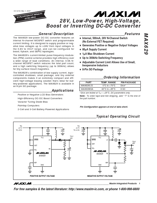
28V, Low-Power, High-Voltage, Boost or Inverting DC-DC Converter MAX629
Stresses beyond those listed under “Absolute Maximum Ratings” may cause permanent damage to the device. These are stress ratings only, and functional operation of the device at these or any other conditions beyond those indicated in the operational sections of the specifications is not implied. Exposure to absolute maximum rating conditions for extended periods may affect device reliability.
元器件交易网
19-1219; Rev 1; 6/97
ANUAL N KIT M IO T A U EVAL BLE AVAILA
28V, Low-Power, High-Voltage, Boost or Inverting DC-DC Converter
____________________________Features
___________________________________________________Typical Operating Circuit
MAX6368PKA23-T中文资料
MAX6365–MAX6368
SOT23, Low-Power µP Supervisory Circuits with Battery Backup and Chip-Enable Gating
ABSOLUTE MAXIMUM RATINGS
Terminal Voltages (with respect to GND)
SOT23 Pin Configurations continued at end of data sheet.
Typical Operating Circuit appears at end of data sheet.
________________________________________________________________ Maxim Integrated Products 1
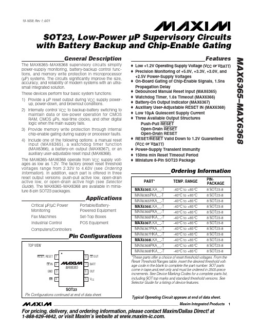
Pin Configurations
TOP VIEW
RESET, RESET 1 CE IN 2 GND 3 MR 4
MAX6365
8 CE OUT 7 BATT 6 OUT 5 VCC
Features
o Low +1.2V Operating Supply Voltage (VCC or VBATT) o Precision Monitoring of +5.0V, +3.3V, +3.0V, and
VCC, BATT, OUT.......................................................-0.3V to +6V RESET (open drain), RESET (open drain) ................-0.3V to +6V BATT ON, RESET (push-pull), RESET IN,
MAX1180ECM中文资料

Features
o Single +3.3V Operation o Excellent Dynamic Performance: 58.5dB SNR at fIN = 20MHz 72dB SFDR at fIN = 20MHz o SNR Flat within 1dB for fIN = 202MHz to 100MHz o Low Power: 125mA (Normal Operation) 2.8mA (Sleep Mode) 1µA (Shutdown Mode) o 0.02dB Gain and 0.25° Phase Matching (typ) o Wide ±1Vp-p Differential Analog Input Voltage Range o 400MHz, -3dB Input Bandwidth o On-Chip +2.048V Precision Bandgap Reference o User-Selectable Output Format—Two’s Complement or Offset Binary o 48-Pin TQFP Package with Exposed Pad for Improved Thermal Dissipation
Stresses beyond those listed under “Absolute Maximum Ratings” may cause permanent damage to the device. These are stress ratings only, and functional operation of the device at these or any other conditions beyond those indicated in the operational sections of the specifications is not implied. Exposure to absolute maximum rating conditions for extended periods may affect device reliability.
MAX9378EUA中文资料

19-2846; Rev 1; 7/03
Anything-to-LVPECL/LVDS Translators with Pin-Selectable Divide-by-Four
General Description
The MAX9377/MAX9378 are fully differential, highspeed, low-jitter anything-to-LVPECL and anything-toLVDS translators, respectively, with a selectable divide-by-four function. Low propagation delay and high speed make them ideal for various high-speed network routing and backplane applications at speeds up to 2GHz in nondivide mode. The MAX9377/MAX9378 accept any differential input signal within the supply rails and with minimum amplitude of 100mV. Inputs are fully compatible with the LVDS, LVPECL, HSTL, and CML differential signaling standards. The MAX9377 outputs are LVPECL and have sufficient current to drive 50Ω transmission lines. The MAX9378 outputs are LVDS and conform to the ANSI EIA/TIA-644 LVDS standard. The MAX9377/MAX9378 are available in 8-pin µMAX packages and operate from a single +3.3V supply over the -40°C to +85°C temperature range.
MAX6387XS18D7中文资料
MAX6387XS18D7中⽂资料General Description The MAX6381–MAX6390 microprocessor (µP) supervisory circuits monitor power-supply voltages from +1.8V to +5.0V while consuming only 3µA of supply current at +1.8V. Whenever V CC falls below the factory-set reset thresholds, the reset output asserts and remains assert-ed for a minimum reset timeout period after V CC rises above the reset threshold. Reset thresholds are available from +1.58V to +4.63V, in approximately 100mV incre-ments. Seven minimum reset timeout delays ranging from 1ms to 1200ms are available.The MAX6381/MAX6384/MAX6387 have a push-pull active-low reset output. The MAX6382/MAX6385/ MAX6388 have a push-pull active-high reset output, and the MAX6383/MAX6386/MAX6389/MAX6390 have an open-drain active-low reset output. The MAX6384/MAX6385/MAX6386 also feature a debounced manual reset input (with internal pullup resistor). The MAX6387/MAX6388/MAX6389 have an auxiliary input for monitoring a second voltage. The MAX6390 offers a manual reset input with a longer V CC reset timeout period (1120ms or 1200ms) and a shorter manual reset timeout (140ms or 150ms). The MAX6381/MAX6382/MAX6383 are available in 3-pin SC70 and6-pinµDFN packages and the MAX6384–MAX6390 are available in 4-pin SC70 andFeaturesFactory-Set Reset Threshold Voltages Rangingfrom +1.58V to +4.63V in Approximately 100mVIncrements±2.5% Reset Threshold Accuracy OverTemperature (-40°C to +125°C)Seven Reset Timeout Periods Available: 1ms,20ms, 140ms, 280ms, 560ms, 1120ms,1200ms (min)3 Reset Output OptionsActive-Low Push-PullActive-High Push-PullActive-Low Open-DrainReset Output State Guaranteed ValidDown to V CC= 1VManual Reset Input (MAX6384/MAX6385/MAX6386)Auxiliary RESET IN(MAX6387/MAX6388/MAX6389)V CC Reset Timeout (1120ms or 1200ms)/ManualReset Timeout (140ms or 150ms) (MAX6390)Negative-Going V CC Transient ImmunityLow Power Consumption of 6µA at +3.6Vand 3µA at +1.8VPin Compatible withMAX809/MAX810/MAX803/MAX6326/MAX6327/MAX6328/MAX6346/MAX6347/MAX6348,and MAX6711/MAX6712/MAX6713Tiny 3-Pin/4-Pin SC70 and 6-Pin µDFN PackagesMAX6381–MAX6390 SC70/µDFN, Single/Dual Low-Voltage,Low-Power µP Reset Circuits ________________________________________________________________Maxim Integrated Products1Pin Configurations19-1839; Rev 4; 4/07Ordering InformationOrdering Information continued at end of data sheet.Typi cal Operati ng Ci rcui t appears at end of data sheet.Selector Guide appears at end of data sheet.after "XR", "XS", or "LT." Insert reset timeout delay (see ResetTimeout Delay table) after "D" to complete the part number.Sample stock is generally held on standard versions only (seeStandard Versions table). Standard versions have an orderincrement requirement of 2500 pieces. Nonstandard versionshave an order increment requirement of 10,000 pieces.Contact factory for availability of nonstandard versions.+Denotes a lead-free package.For pricing, delivery, and ordering information,please contact Maxim Direct at 1-888-629-4642,or visit Maxim’s website at /doc/5700977901f69e3143329415.html .ComputersControllersIntelligent InstrumentsCritical µP and µCPower MonitoringPortable/Battery-Powered EquipmentDual Voltage SystemsM A X 6381–M A X 6390SC70/µDFN, Single/Dual Low-Voltage, Low-Power µP Reset CircuitsABSOLUTE MAXIMUM RATINGSELECTRICAL CHARACTERISTICS(V CC = full range, T A = -40°C to +125°C, unless otherwise specified. Typical values are at T A = +25°C.) (Note 1)Stresses beyond those listed under “Absolute Maximum Ratings” may cause permanent damage to the device. These are stress ratings only, and functional operation of the device at these or any other conditions beyond those indicated in the operational sections of the specifications is not implied. Exposure to absolute maximum rating conditions for extended periods may affect device reliability.V CC to GND..........................................................-0.3V to +6.0V RESET Open-Drain Output....................................-0.3V to +6.0V RESET , RESET (push-pull output)..............-0.3V to (V CC + 0.3V)MR , RESET IN.............................................-0.3V to (V CC + 0.3V)Input Current (V CC ).............................................................20mA Output Current (all pins).....................................................20mAContinuous Power Dissipation (T A = +70°C)3-Pin SC70 (derate 2.9mW/°C above +70°C)..............235mW 4-Pin SC70 (derate 3.1mW/°C above +70°C)..............245mW 6-Pin µDFN (derate 2.1mW/°C above +70°C)..........167.7mW Operating Temperature Range .........................-40°C to+125°C Storage Temperature Range.............................-65°C to +150°C Lead Temperature (soldering,10s).................................+300°CMAX6381–MAX6390SC70/µDFN, Single/Dual Low-Voltage,Low-Power µP Reset Circuits_______________________________________________________________________________________3M A X 6381–M A X 6390SC70/µDFN, Single/Dual Low-Voltage, Low-Power µP Reset Circuits4______________________________________________________________________________________Typical Operating Characteristics(T A = +25°C, unless otherwise noted.)215436789-40-105-25203550658095110125SUPPLY CURRENT vs. TEMPERATURE(NO LOAD)TEMPERATURE (°C)S U P P L Y C U R R E N T (µA )25292735333137394143-40-105-25203550658095110125POWER-DOWN RESET DELAYvs. TEMPERATURETEMPERATURE (°C)P O W E R -D O W N R E S E T D E L A Y (µs )0.940.980.961.021.001.061.041.08-40-10520-253550658095110125 NORMALIZED POWER-UP RESET TIMEOUTvs. TEMPERATUREM A X 6381/90 t o c 03TEMPERATURE (°C)N O R M A L I Z E D R E S E T T I M E O U T P E R I O D0.9900.9851.0150.9950.9901.0001.0051.0101.020-40-10520-253550958011065125 M A X 6381/90 t o c 04TEMPERATURE (°C)N O R M A L I Z E D R E S E T TH R E S H O L D NORMALIZED RESET THRESHOLDvs. TEMPERATURE00.40.20.80.61.01.2063912OUTPUT-VOLTAGE LOW vs. SINK CURRENTI SINK (mA)V O L (V )01.00.52.01.52.53.00500750250100012501500OUTPUT-VOLTAGE HIGH vs. SOURCE CURRENTI SOURCE (µA)V O H (V )45001100010010MAXIMUM TRANSIENT DURATION vs. RESET COMPARATOR OVERDRIVE15050350250500200100400300RESET COMPARATOR OVERDRIVE, V TH - V CC (mV)M A X I M U M T R A N S I E N T D U R A T I O N (µs )3.53.93.74.54.34.14.74.95.35.15.5-40-105-25203550658095110125RESET IN TO RESET DELAYvs. TEMPERATUREM A X 6381/90 t o c 08TEMPERATURE (°C)R E S E T I N D E L A Y (µs )MAX6381–MAX6390SC70/µDFN, Single/Dual Low-Voltage,Low-Power µP Reset CircuitsPin DescriptionM A X 6381–M A X 6390SC70/µDFN, Single/Dual Low-Voltage, Low-Power µP Reset Circuits6_______________________________________________________________________________________ Detailed DescriptionRESET OutputA µP reset input starts the µP in a known state. These µP supervisory circuits assert reset to prevent code execution errors during power-up, power-down, or brownout conditions.Reset asserts when V CC is below the reset threshold;once V CC exceeds the reset threshold, an internal timer keeps the reset output asserted for the reset timeout period. After this interval, reset output deasserts. Reset output is guaranteed to bein the correct logic state for V CC ≥1V.Manual Reset Input (MAX6384/MAX6385/MAX6386/MAX6390)Many µP-based products require manual reset capabil-ity, allowing the operator, a test technician, or external logic circuitry to initiate a reset. A logic low on MR asserts reset. Reset remains asserted while MR is low,and for the reset active timeout period (t RP ) after MR returns high. This input has an internal 63k ?pullup resistor (1.56k ?for MAX6390), so it can be left uncon-nected if it is not used. MR can be driven with TTL or CMOS logic levels, or with open-drain/collector outputs.Connect a normally open momentary switch from MR to G ND to create a manual-reset function; external debounce circuitry is not required. If MR is driven from long cables or if the device is used in a noisy environ-ment, connecting a 0.1µF capacitor from MR to G ND provides additional noise immunity.RESET IN Comparator(MAX6387/MAX6388/MAX6389)RESET IN is compared to an internal +1.27V reference.If the voltage at RESET IN is less than 1.27V, reset asserts. Use the RESET IN comparator as a user-adjustable reset detector or as a secondary power-sup-ply monitor by implementing a resistor-divider at RESET IN (shown in Figure 1). Reset asserts when either V CC or RESET IN falls below its respective threshold volt-age. Use the following equation to set the threshold:V INTH = V THRST (R1/R2 + 1)where V THRST = +1.27V. To simplify the resistor selec-tion, choose a value of R2 and calculate R1:R1 = R2 [(V INTH /V THRST ) - 1]Since the input current at RESET IN is 50nA (max),large values can be used for R2 with no significant loss in accuracy.___________Applications InformationNegative-Going V CC TransientsIn addition to issuing a reset to the µP during power-up,power-down, and brownout conditions, the MAX6381–MAX6390 are relatively immune to short dura-tion negative-going V CC transients (glitches).The Typical Operating Characteristics section shows the Maximum Transient Durations vs. Reset Comparator Overdrive, for which the MAX6381–MAX6390 do not generate a reset pulse. This graph was generated usinga negative-going pulse applied to V CC , starting above the actual reset threshold and ending below it by the magnitude indicated (reset comparator overdrive). The graph indicates the typical maximum pulse width a neg-ative-going V CC transient may have without causing a reset pulse to be issued. As the magnitude of the tran-sient increases (goes farther below the reset threshold),the maximum allowable pulse width decreases. A 0.1µF capacitor mounted as close as possible to V CC provides additional transient immunity.Ensuring a Valid RESET Output Down to V CC = 0VThe MAX6381–MAX6390 are guaranteed to operate properly down to V CC = 1V. In applications that require valid reset levels down to V CC = 0V, a pulldown resistor to active-low outputs (push/pull only, Figure 2) and a pullup resistor to active-high outputs (push/pull only)will ensure that the reset line is valid while the reset out-put can no longer sink or source current. This schemedoes not work with the open-drain outputs of the MAX6383/MAX6386/MAX6389/MAX6390. The resistor value used is not critical, but it must be small enough not to load the reset output when V CC is above the reset threshold. For most applications, 100k ?is ade-quate.MAX6381–MAX6390SC70/µDFN, Single/Dual Low-Voltage,Low-Power µP Reset Circuits_______________________________________________________________________________________7M A X 6381–M A X 6390SC70/µDFN, Single/Dual Low-Voltage, Low-Power µP Reset Circuits 8_______________________________________________________________________________________ Selector GuideOrdering Information (continued)Note:Insert reset threshold suffix (see Reset Threshold table)after "XR", "XS", or "LT." Insert reset timeout delay (see Reset Timeout Delay table) after "D" to complete the part number.Sample stock is generally held on standard versions only (see Standard Versions table). Standard versions have an order increment requirement of 2500 pieces. Nonstandard versions have an order increment requirement of 10,000 pieces.Contact factory for availability of nonstandard versions.*MAX6390 is available with D4 or D7 timing only.+Denotes a lead-free package.MAX6381–MAX6390SC70/µDFN, Single/Dual Low-Voltage,Low-Power µP Reset Circuits_______________________________________________________________________________________9Chip InformationTRANSISTOR COUNT: 647PROCESS: BiCMOSPin Configurations (continued)M A X 6381–M A X 6390SC70/µDFN, Single/Dual Low-Voltage, Low-Power µP Reset Circuits10______________________________________________________________________________________ Package Information(The package drawing(s) in this data sheet may not reflect the most current specifications. For the latest package outline information,go to /doc/5700977901f69e3143329415.html /packages .)MAX6381–MAX6390SC70/µDFN, Single/Dual Low-Voltage,Low-Power µP Reset Circuits______________________________________________________________________________________11Package Information (continued)(The package drawing(s) in this data sheet may not reflect the most current specifications. For the latest package outline information,go to /doc/5700977901f69e3143329415.html /packages .)M A X 6381–M A X 6390SC70/µDFN, Single/Dual Low-Voltage, Low-Power µP Reset Circuits12______________________________________________________________________________________ Package Information (continued)(The package drawing(s) in this data sheet may not reflect the most current specifications. For the latest package outline information,go to /doc/5700977901f69e3143329415.html /packages .)SC70/µDFN, Single/Dual Low-Voltage,Low-Power µP Reset CircuitsMaxim cannot assume responsibility for use of any circuitry other than circuitry entirely embodied in a Maxim product. No circuit patent licenses are implied. Maxim reserves the right to change the circuitry and specifications without notice at any time.Maxim Integrated Products, 120 San Gabriel Drive, Sunnyvale, CA 94086 408-737-7600____________________13?2007 Maxim Integrated Productsis a registered trademark of Maxim Integrated Products, Inc.MAX6381–MAX6390Package Information (continued)(The package drawing(s) in this data sheet may not reflect the most current specifications. For the latest package outline information,go to /doc/5700977901f69e3143329415.html /packages .)Revision HistoryPages changed at Rev 4: Title on all pages, 1, 2, 5,7–13。
MAX333AEWP中文资料

________________________________________________________________ Maxim Integrated Products
1
For free samples & the latest literature: , or phone 1-800-998-8800. For small orders, phone 1-800-835-8769.
元器件交易网
Precision, Quad, SPDT, CMOS Analog Switch MAX333A
ABSOLUTE MAXIMUM RATINGS
V+ to V- ..................................................................................44V VIN, VCOM, VNO, VNC ......................................................V- to V+ (VNO - VNC) ............................................................................32V V+ to Ground..........................................................................30V V- to Ground..........................................................................-30V Current, Any Terminal Except VCOM, VNO, or VNC .............30mA Continuous Current, VCOM, VNO, or VNC ............................20mA Peak Current, VCOM, VNO, or VNC (Pulsed at 1ms, 10% duty cycle max) ............................70mA ESD ....................................................................................2000V Note 1: Device mounted with all leads soldered to PC board. Continuous Power Dissipation (TA = +70°C) (Note 1) Plastic DIP (derate above +70°C by 11.11mW/°C) .....889mW SO (derate above +70°C by 10.00mW/°C) ..................800mW CERDIP (derate above +70°C by 11.11mW/°C) ..........889mW TSSOP (derate above +70°C by 7mW/°C) ..................559mW Operating Temperature Ranges: MAX333AC_ _ .....................................................0°C to +70°C MAX333AE_ _ ..................................................-40°C to +85°C MAX333AMJP ................................................-55°C to +125°C Storage Temperature Range .............................-65°C to +150°C Lead Temperature (soldering, 10sec) .............................+300°C
MAX1236KEUA+中文资料

Features
♦ High-Speed I2C-Compatible Serial Interface ♦ ♦ ♦ ♦ ♦ ♦ ♦ ♦ 400kHz Fast Mode 1.7MHz High-Speed Mode Single-Supply 2.7V to 3.6V (MAX1237/MAX1239) 4.5V to 5.5V (MAX1236/MAX1238) Internal Reference 2.048V (MAX1237/MAX1239) 4.096V (MAX1236/MAX1238) External Reference: 1V to VDD Internal Clock 4-Channel Single-Ended or 2-Channel Fully Differential (MAX1236/MAX1237) 12-Channel Single-Ended or 6-Channel Fully Differential (MAX1238/MAX1239) Internal FIFO with Channel-Scan Mode Low Power 670µA at 94.4ksps 230µA at 40ksps 60µA at 10ksps 6µA at 1ksps 0.5µA in Power-Down Mode Software-Configurable Unipolar/Bipolar Small Packages 8-Pin µMAX (MAX1236/MAX1237) 16-Pin QSOP (MAX1238/MAX1239)
元器件交易网
19-2333; Rev 4; 9/06
2.7V to 3.6V and 4.5V to 5.5V, Low-Power, 4-/12-Channel, 2-Wire Serial, 12-Bit ADCs
- 1、下载文档前请自行甄别文档内容的完整性,平台不提供额外的编辑、内容补充、找答案等附加服务。
- 2、"仅部分预览"的文档,不可在线预览部分如存在完整性等问题,可反馈申请退款(可完整预览的文档不适用该条件!)。
- 3、如文档侵犯您的权益,请联系客服反馈,我们会尽快为您处理(人工客服工作时间:9:00-18:30)。
___________________________________________________________________Selector Guide________________General DescriptionThe MAX6316–MAX6322 family of microprocessor (µP)supervisory circuits monitors power supplies and microprocessor activity in digital systems. It offers sev-eral combinations of push/pull, open-drain, and bidirec-tional (such as Motorola 68HC11) reset outputs, along with watchdog and manual reset features. The Selector Guide below lists the specific functions available from each device. These devices are specifically designed to ignore fast negative transients on V CC . Resets are guaranteed valid for V CC down to 1V.These devices are available in 26 factory-trimmed reset threshold voltages (from 2.5V to 5V, in 100mV incre-ments), featuring four minimum power-on reset timeout periods (from 1ms to 1.12s), and four watchdog timeout periods (from 6.3ms to 25.6s). Thirteen standard ver-sions are available with an order increment requirement of 2500 pieces (see Standard Versions table); contact the factory for availability of other versions, which have an order increment requirement of 10,000 pieces.The MAX6316–MAX6322 are offered in a miniature 5-pin SOT23 package.________________________ApplicationsPortable Computers Computers ControllersIntelligent InstrumentsPortable/Battery-Powered Equipment Embedded Control Systems____________________________Features♦Small 5-Pin SOT23 Package♦Available in 26 Reset Threshold Voltages2.5V to 5V, in 100mV Increments ♦Four Reset Timeout Periods1ms, 20ms, 140ms, or 1.12s (min)♦Four Watchdog Timeout Periods6.3ms, 102ms, 1.6s, or 25.6s (typ) ♦Four Reset Output StagesActive-High, Push/Pull Active-Low, Push/Pull Active-Low, Open-Drain Active-Low, Bidirectional♦Guaranteed Reset Valid to V CC = 1V♦Immune to Short Negative V CC Transients ♦Low Cost♦No External ComponentsMAX6316–MAX63225-Pin µP Supervisory Circuits withWatchdog and Manual Reset________________________________________________________________Maxim Integrated Products 119-0496; Rev 7; 11/07_______________Ordering InformationOrdering Information continued at end of data sheet.*The MAX6318/MAX6319/MAX6321/MAX6322 feature two types of reset output on each device.Typical Operating Circuit and Pin Configurations appear at end of data sheet.For pricing, delivery, and ordering information, please contact Maxim Direct at 1-888-629-4642,or visit Maxim’s website at .Specify lead-free by replacing “-T” with “+T” when ordering.ELECTRICAL CHARACTERISTICS(V CC = 2.5V to 5.5V, T A = -40°C to +125°C, unless otherwise noted. Typical values are at T A = +25°C.) (Note 1)M A X 6316–M A X 63225-Pin µP Supervisory Circuits with Watchdog and Manual Reset 2_______________________________________________________________________________________ABSOLUTE MAXIMUM RATINGSStresses beyond those listed under “Absolute Maximum Ratings” may cause permanent damage to the device. These are stress ratings only, and functional operation of the device at these or any other conditions beyond those indicated in the operational sections of the specifications is not implied. Exposure to absolute maximum rating conditions for extended periods may affect device reliability.Voltage (with respect to GND)V CC ......................................................................-0.3V to +6V RESET (MAX6320/MAX6321/MAX6322 only)...... -0.3V to +6V All Other Pins.........................................-0.3V to (V CC + 0.3V)Input/Output Current, All Pins.............................................20mAContinuous Power Dissipation (T A = +70°C)SOT23-5 (derate 7.1mW/°C above +70°C)...............571mW Operating Temperature Range..........................-40°C to +125°C Junction Temperature......................................................+150°C Storage Temperature Range..............................-65°C to +160°C Lead Temperature (soldering, 10s).................................+300°CTH available in 100mV increments from 2.5V to 5V (see Table 1 at end of data sheet).Note 3:Guaranteed by design.MAX6316–MAX63225-Pin µP Supervisory Circuits withWatchdog and Manual Reset_______________________________________________________________________________________3Note 5:Measured from RESET V OL to (0.8 x V CC ), R LOAD = ∞.Note 6:WDI is internally serviced within the watchdog period if WDI is left unconnected.Note 7:The WDI input current is specified as the average input current when the WDI input is driven high or low. The WDI input is designed for a three-stated-output device with a 10µA maximum leakage current and capable of driving a maximum capac-itive load of 200pF. The three-state device must be able to source and sink at least 200µA when active.ELECTRICAL CHARACTERISTICS (continued)M A X 6316–M A X 63225-Pin µP Supervisory Circuits with Watchdog and Manual Reset 4_________________________________________________________________________________________________________________________________Typical Operating Characteristics(T A = +25°C, unless otherwise noted.)021*********-4020-20406080100MAX6316/MAX6317/MAX6318/MAX6320/MAX6321SUPPLY CURRENT vs. TEMPERATURETEMPERATURE (°C)S U P P L Y C U R R E N T (μA )302010504090807060100-40-20020406080100V CC FALLING TO RESET PROPAGATIONDELAY vs. TEMPERATURETEMPERATURE (°C)R E S E T P R O P A G A T I O N D E L A Y (μs )140180160240220200300280260320-40020-20406080100MAX6316/MAX6317/MAX6319/MAX6320/MAX6322MANUAL RESET TO RESETPROPAGATION DELAY vs. TEMPERATURETEMPERATURE (°C)P R O P A G A T I O N D E L A Y (n s )0.950.980.970.961.000.991.041.031.021.011.05-40-2020406080100NORMALIZED RESET TIMEOUT PERIOD vs. TEMPERATUREM A X 6316t o c 04TEMPERATURE (°C)N O R M A L I Z E D R E S E T T I M E O U T P E R I O D0.950.980.970.961.000.991.041.031.021.011.05-40-2020406080100MAX6316/MAX6317/MAX6318/MAX6320/MAX6321NORMALIZED WATCHDOG TIMEOUTPERIOD vs. TEMPERATUREM A X 6316t o c 05TEMPERATURE (°C)N O R M A L I Z E D W A T C H D O G T I M E O U T P E R I O D800101001000MAXIMUM V CC TRANSIENT DURATION vs. RESET THRESHOLD OVERDRIVE2010RESET THRESHOLD OVERDRIVE (mV) V RST - V CCT RA N S I E N T D U R A T I O N (μs )3050604070200ns/divMAX6316M/6318MH/6319MHBIDIRECTIONALPULLUP CHARACTERISTICSMAX6316–MAX63225-Pin µP Supervisory Circuits withWatchdog and Manual Reset_______________________________________________________________________________________5______________________________________________________________Pin DescriptionM A X 6316–M A X 63225-Pin µP Supervisory Circuits with Watchdog and Manual Reset 6______________________________________________________________________________________________________Detailed DescriptionA microprocessor’s (µP) reset input starts or restarts the µP in a known state. The reset output of the MAX6316–MAX6322 µP supervisory circuits interfaces with the reset input of the µP, preventing code-execution errors during power-up, power-down, and brownout condi-tions (see the Typical Operating Circuit ). The MAX6316/MAX6317/MAX6318/MAX6320/MAX6321 are also capa-ble of asserting a reset should the µP become stuck in an infinite loop.Reset OutputThe MAX6316L/MAX6318LH/MAX6319LH feature an active-low reset output, while the MAX6317H/MAX6318_H/MAX6319_H/MAX6321HP/MAX6322HP feature an active-high reset output. RESET is guaran-teed to be a logic low and RESET is guaranteed to be a logic high for V CC down to 1V.The MAX6316–MAX6322 assert reset when V CC is below the reset threshold (V RST ), when MR is pulled low (MAX6316_/MAX6317H/MAX6319_H/MAX6320P/MAX6322HP only), or if the WDI pin is not serviced withinthe watchdog timeout period (t WD ). Reset remains assert-ed for the specified reset active timeout period (t RP ) after V CC rises above the reset threshold, after MR transitions low to high, or after the watchdog timer asserts the reset (MAX6316_/MAX6317H/MAX6318_H/MAX6320P/MAX6321HP). After the reset active timeout period (t RP )expires, the reset output deasserts, and the watchdog timer restarts from zero (Figure 2).Figure 1. Functional DiagramFigure 2. Reset Timing DiagramMAX6316–MAX63225-Pin µP Supervisory Circuits withWatchdog and Manual Reset_______________________________________________________________________________________7Bidirectional R E S E T OutputThe MAX6316M/MAX6318MH/MAX6319MH are designed to interface with µPs that have bidirectional reset pins,such as the Motorola 68HC11. Like an open-drain output,these devices allow the µP or other devices to pull the bidirectional reset (RESET ) low and assert a reset condi-tion. However, unlike a standard open-drain output, it includes the commonly specified 4.7k Ωpullup resistor with a P-channel active pullup in parallel.This configuration allows the MAX6316M/MAX6318MH/MAX6319MH to solve a problem associated with µPs that have bidirectional reset pins in systems where sev-eral devices connect to RESET (F igure 3). These µPs can often determine if a reset was asserted by an exter-nal device (i.e., the supervisor IC) or by the µP itself (due to a watchdog fault, clock error, or other source),and then jump to a vector appropriate for the source of the reset. However, if the µP does assert reset, it does not retain the information, but must determine the cause after the reset has occurred.The following procedure describes how this is done in the Motorola 68HC11. In all cases of reset, the µP pulls RESET low for about four external-clock cycles. It then releases RESET , waits for two external-clock cycles,then checks RESET ’s state. If RESET is still low, the µP concludes that the source of the reset was external and, when RESET eventually reaches the high state, it jumps to the normal reset vector. In this case, stored-state information is erased and processing begins fromscratch. If, on the other hand, RESET is high after a delay of two external-clock cycles, the processor knows that it caused the reset itself and can jump to a different vector and use stored-state information to determine what caused the reset.A problem occurs with faster µPs; two external-clock cycles are only 500ns at 4MHz. When there are several devices on the reset line, and only a passive pullup resis-tor is used, the input capacitance and stray capacitance can prevent RESET from reaching the logic high state (0.8✕V CC ) in the time allowed. If this happens, all resets will be interpreted as external. The µP output stage is guaran-teed to sink 1.6mA, so the rise time can not be reduced considerably by decreasing the 4.7k Ωinternal pullup resistance. See Bidirectional Pullup Characteristics in the Typical Operating Characteristics .The MAX6316M/MAX6318MH/MAX6319MH overcome this problem with an active pullup FET in parallel with the 4.7k Ωresistor (F igures 4 and 5). The pullup transistor holds RESET high until the µP reset I/O or the supervisory circuit itself forces the line low. Once RESET goes below V PTH , a comparator sets the transition edge flip-flop, indi-cating that the next transition for RESET will be low to high. When RESET is released, the 4.7k Ωresistor pulls RESET up toward V CC . Once RESET rises above V PTH but is below (0.85 x V CC ), the active P-channel pullup turns on. Once RESET rises above (0.85 x V CC ) or the 2µs one-shot times out, the active pullup turns off. The parallel combination of the 4.7k Ωpullup and theFigure 3. MAX6316M/MAX6318MH/MAX6319MH Supports Additional Devices on the Reset BusM A X 6316–M A X 63225-Pin µP Supervisory Circuits with Watchdog and Manual Reset 8_______________________________________________________________________________________Figure 4. MAX6316/MAX6318MH/MAX6319MH Bidirectional Reset Output Functional DiagramMAX6316–MAX63225-Pin µP Supervisory Circuits withWatchdog and Manual Reset_______________________________________________________________________________________9P-channel transistor on-resistance quickly charges stray capacitance on the reset line, allowing RESET to transition from low to high within the required two elec-tronic-clock cycles, even with several devices on the reset line. This process occurs regardless of whether the reset was caused by V CC dipping below the reset threshold, the watchdog timing out, MR being asserted,or the µP or other device asserting RESET . The parts do not require an external pullup. To minimize supply cur-rent consumption, the internal 4.7k Ωpullup resistor dis-connects from the supply whenever the MAX6316M/MAX6318MH/MAX6319MH assert reset.Open-Drain R E S E T OutputThe MAX6320P/MAX6321HP/MAX6322HP have an active-low, open-drain reset output. This output struc-ture will sink current when RESET is asserted. Connect a pullup resistor from RESET to any supply voltage up to 6V (Figure 6). Select a resistor value large enough toregister a logic low (see Electrical Characteristics ), and small enough to register a logic high while supplying all input current and leakage paths connected to the RESET line. A 10k Ωpullup is sufficient in most applications.Manual-Reset InputThe MAX6316_/MAX6317H/MAX6319_H/MAX6320P/MAX6322HP feature a manual reset input. A logic low on MR asserts a reset. After MR transitions low to high, reset remains asserted for the duration of the reset timeout peri-od (t RP ). The MR input is connected to V CC through an internal 52k Ωpullup resistor and therefore can be left unconnected when not in use. MR can be driven with TTL-logic levels in 5V systems, with CMOS-logic levels in 3V systems, or with open-drain or open-collector output devices. A normally-open momentary switch from MR to ground can also be used; it requires no external debouncing circuitry. MR is designed to reject fast, negative-going transients (typically 100ns pulses). A 0.1µF capacitor from MR to ground provides additional noise immunity.The MR input pin is equipped with internal ESD-protection circuitry that may become forward biased. Should MR be driven by voltages higher than V CC , excessive current would be drawn, which would damage the part. F or example, assume that MR is driven by a +5V supply other than V CC . If V CC drops lower than +4.7V, MR ’s absolute maximum rating is violated [-0.3V to (V CC + 0.3V)], and undesirable current flows through the ESD structure from MR to V CC . To avoid this, use the same supply for MR as the supply monitored by V CC . This guarantees that the voltage at MR will never exceed V CC .Watchdog InputThe MAX6316_/MAX6317H/MAX6318_H/MAX6320P/MAX6321HP feature a watchdog circuit that monitors the µP’s activity. If the µP does not toggle the watchdog input (WDI) within the watchdog timeout period (t WD ),reset asserts. The internal watchdog timer is cleared by reset or by a transition at WDI (which can detect pulses as short as 50ns). The watchdog timer remains cleared while reset is asserted. Once reset is released, the timer begins counting again (Figure 7).The WDI input is designed for a three-stated output device with a 10µA maximum leakage current and the capability of driving a maximum capacitive load of 200pF.The three-state device must be able to source and sink at least 200µA when active. Disable the watchdog function by leaving WDI unconnected or by three-stating the driver connected to WDI. When the watchdog timer is left open circuited, the timer is cleared internally at intervals equal to 7/8 of the watchdog period.Figure 6. MAX6320P/MAX6321HP/MAX6322HP Open-Drain RESET Output Allows Use with Multiple SuppliesFigure 5. Bidirectional RESET Timing DiagramM A X 6316–M A X 63225-Pin µP Supervisory Circuits with Watchdog and Manual Reset 10______________________________________________________________________________________Applications InformationWatchdog Input CurrentThe WDI input is internally driven through a buffer and series resistor from the watchdog counter. For minimum watchdog input current (minimum overall power con-sumption), leave WDI low for the majority of the watch-dog timeout period. When high, WDI can draw as much as 160µA. Pulsing WDI high at a low duty cycle will reduce the effect of the large input current. When WDI is left unconnected, the watchdog timer is serviced within the watchdog timeout period by a low-high-low pulse from the counter chain.Negative-Going V CC TransientsThese supervisors are immune to short-duration, nega-tive-going V CC transients (glitches), which usually do not require the entire system to shut down. Typically,200ns large-amplitude pulses (from ground to V CC ) on the supply will not cause a reset. Lower amplitude puls-es result in greater immunity. Typically, a V CC transient that goes 100mV under the reset threshold and lasts less than 4µs will not trigger a reset. An optional 0.1µF bypass capacitor mounted close to V CC provides addi-tional transient immunity.Ensuring Valid Reset OutputsDown to V CC = 0The MAX6316_/MAX6317H/MAX6318_H/MAX6319_H/MAX6321HP/MAX6322HP are guaranteed to operate properly down to V CC = 1V. In applications that require valid reset levels down to V CC = 0, a pulldown resistor to active-low outputs (push/pull and bidirectional only,F igure 8) and a pullup resistor to active-high outputs(push/pull only, Figure 9) will ensure that the reset line is valid while the reset output can no longer sink orsource current. This scheme does not work with the open-drain outputs of the MAX6320/MAX6321/MAX6322.The resistor value used is not critical, but it must be large enough not to load the reset output when V CC is above the reset threshold. F or most applications,100k Ωis adequate.Watchdog Software Considerations(MAX6316/MAX6317/MAX6318/MAX6320/MAX6321)One way to help the watchdog timer monitor software execution more closely is to set and reset the watchdog input at different points in the program, rather than pulsing the watchdog input high-low-high or low-high-low. This technique avoids a stuck loop, in which the watchdog timer would continue to be reset inside the loop, keeping the watchdog from timing out.Figure 7. Watchdog Timing RelationshipFigure 9. Ensuring RESET Valid to V CC = 0 on Active-High Push/Pull OutputsFigure 8. Ensuring RESET Valid to V CC = 0 on Active-Low Push/Pull and Bidirectional OutputsMAX6316–MAX6322Watchdog and Manual Reset______________________________________________________________________________________11F igure 10 shows an example of a flow diagram where the I/O driving the watchdog input is set high at the beginning of the program, set low at the end of every subroutine or loop, then set high again when the pro-gram returns to the beginning. If the program should hang in any subroutine, the problem would be quickly corrected, since the I/O is continually set low and the watchdog timer is allowed to time out, causing a reset or interrupt to be issued. As described in the Watchdog Input Current section, this scheme results in higher time average WDI current than does leaving WDI low for the majority of the timeout period and periodically pulsing it low-high-low.Figure 10. Watchdog Flow Diagram__________________Pin ConfigurationsTypical Operating CircuitTable 2. Standard VersionsTable 1. Factory-Trimmed Reset ThresholdsM A X 6316–M A X 6322Watchdog and Manual ResetTable 3. Reset/Watchdog Timeout PeriodsMAX6316–MAX6322Watchdog and Manual Reset______________________________________________________________________________________13__Ordering Information (continued)a watchdog feature (see Selector Guide) are factory-trimmed to one of four watchdog timeout periods. Insert the letter corre-sponding to the desired watchdog timeout period (W, X, Y, or Z from Table 3) into the blank following the reset timeout suffix.TRANSISTOR COUNT: 191SUBSTRATE IS INTERNALLY CONNECTED TO V+Chip Informationdard versions only. The required order increment for nonstandard versions is 10,000 pieces. Contact factory for availability.M A X 6316–M A X 6322Watchdog and Manual Reset 14______________________________________________________________________________________Package Information(The package drawing(s) in this data sheet may not reflect the most current specifications. For the latest package outline information,go to /packages .)M axim cannot assume responsibility for use of any circuitry other than circuitry entirely embodied in a M axim product. No circuit patent licenses are implied. Maxim reserves the right to change the circuitry and specifications without notice at any time.Maxim Integrated Products, 120 San Gabriel Drive, Sunnyvale, CA 94086 408-737-7600 ____________________15©2007 Maxim Integrated Productsis a registered trademark of Maxim Integrated Products, Inc.MAX6316–MAX6322 Watchdog and Manual ResetRevision History。