C67078-S3132-A2中文资料
AMS3132

General DescriptionThe AMS3132 is a high performance linear regulator with very low dropout voltage and excellent transient response. It is designed to operate with wide input voltage range of 1.5 – 7Volts making it ideal for two step conversion while maintaining high efficiency for many power sensitive applications. The device is capable of supplying 3A of output current with a typical dropout voltage of 700mV at 3A. The product is available in either fixed or adjustable output voltage.The linear regulator has been optimized for noise sensitive applications. The device includes an optional enable pin for electrical on/off of the regulator. Forcing the enable pin to logic low shuts down the LDO and reduces the supply current to less than 1µA.The product includes complete short-circuit and thermal protection. The combination of these two internal protection circuits gives the device a comprehensive safety system to safe guard against extreme adverse operating conditions.The AMS3132 is available in a 5-pin surface mount TO263 package, and it is rated for -40°C to +125°C temperature range.Features•V IN range: 1.5 – 7V•Fixed and Adjustable output voltage as low as 0.6V•3A maximum output current•700mV typical dropout voltage at 3A• Low self noise•Optional Power Good (PG) output•Optional Enable (EN) pin for LDO on/off•125µA typical supply current•PSRR >40dB at 10KHz•Stable with Electrolytic, Tantalum orCeramic capacitors•Current Limit protection• Over-Temperature Shutdown•-40 to +125°C temperature range•Available in a 5-pin surface mount TO-263 package•RoHS & WEEE compliantApplications• Set-top Box•DVD, Blue-ray DVD writers•LCD TVs and LCD monitors•Battery Powered Equipment• Infotainment•Wireless & RF Applications•High Efficiency “Green” Laptops & notebookTypical ApplicationPin Description (TO-263 5-Pin Package)Pin #Symbol Description1ENEnable pin. It controls the electrical on/off of the device. When connected to logic low, the device shuts off and consumes less than 1µA of current. Logic high willresume normal operation.PGPower Good pin. It is an open collector, active high output that indicates thestatus of the output voltage. When output voltage (V OUT) exceeds the PG trip threshold, the PG pin goes in to a high impedance state. When the device is out of regulation or shutdown, the PG pin is pulled low. A 10KΩto 1MΩresistorshould be connected from PG to VOUT.2 VINInput supply Voltage. It powers the internal control circuitry and the internal power switch. Bypass V IN with at ceramic capacitor from this pin to ground.3 GND Groundconnection. 4V OUT OutputVoltage5ADJProvides feedback to error amplifier from the resistive divider that sets the outputvoltage.PGPower Good pin. It is an open collector, active high output that indicates thestatus of the output voltage. When output voltage (V OUT ) exceeds the PG trip threshold, the PG pin goes in to a high impedance state. When the device is out of regulation or shutdown, the PG pin is pulled low. A 10K Ω to 1M Ω resistor should be connected from PG to V OUT .Pin ConfigurationAbsolute Maximum Ratings (1)Maximum Input Supply Voltage (V IN )………......…. ……-0.3V to 15V Enable Voltage (EN)…………..…..……………….……...-0.3V to 15V Power Good (PG).……………..…..……….……………...-0.3V to 15V Adjustable Voltage (ADJ)……………………….………… -0.3V to 3V Storage Temperature Range……………...................-65⁰C to 150⁰C Lead Temperature…………………..………….………..……… 260⁰C Junction Temperature………...………………..…………..…… 125⁰CRecommended Operating Conditions (2)Input Voltage…………………………………….………….. 1.5V to 7V Ambient Operating Temperature………….………… -40⁰C to 125⁰CThermal InformationTO263-5 θJA (3)…………………………....…………...….…...30⁰C/WElectrical CharacteristicsUnless otherwise noted: V IN =3.3V; V OUT =1.8V; C IN =10 µF ; C OUT =22µF; -40⁰C ≤T A =T J ≤85⁰C; T J(Max.)= 125°C; Typical values are T A =25°CParameterSymbolConditionsMin. Typ. Max.UnitsOutput Voltage Accuracy VOUT-3 3 %Adjustable VoltageV ADJ Adjustable V OUT only 0.588 0.6 0.612 V Adjustable pin bias current I ADJ_Bias Adjustable V OUT only 10 100 nA Maximum Output Current I OUT_Max3 A Load Regulation I OUT = 0 – 3A 0.1 %Line Regulation V IN =3.0 – 7.0V; I OUT =100mA0.1 % Supply Current I SUP V IN =3.3V, Io=0A0.6 1 mA Shutdown Current I SHDN V IN =3.3V, V EN =0V <1 3 µACurrent LimitI LIM6 ADropout VoltageV DOI OUT =0.1A; V OUT =95% of V OUT(NOM) 60mVI OUT =1A; V OUT =95% of V OUT(NOM) 220I OUT =2A; V OUT =95% of V OUT(NOM) 420 I OUT =3A; V OUT =95% of V OUT(NOM)700PSRRΔV OUT /ΔV INF =10KHz Io =20mA 40 dB Output Noise Voltage e n BW= 100Hz –100 KHz C OUT = 22µF I OUT = 2.75A125 µV(rms) Enable Threshold LowV EN(L) Optional EN Pin present 1.2 V Enable Threshold High V EN(H) Optional EN Pin present 1.3 V Input Enable Low Current I EN(L) V EN = 0V 0 10 nA Input Enable High Current I EN(H) V EN = 1.5V150 300 nA Power Good Low Threshold V PG % of V OUT PG ON / Opt. PG pin only 89 % Power Good High Threshold V PG % of V OUT PG OFF / Opt. PG pin only97%Power Good Output Low Voltage V PGLIPG_SINK = 500μA, Fault Condition200 300 mV Power Good Leakage Current I PG PG off, V PG = 12V 0.01 μA Thermal ShutdownT SD 145 °C Thermal Shutdown HysteresisT SD_HYS15 °CNotes:1. Stresses above those listed in Absolute Maximum Ratings may cause permanent damage to the device.2. Junction to ambient thermal resistance with the TO-263 package tab soldered to a double side printed circuit board with 2.5 in 2 of (1 oz.) copper area.3.With package soldering to 0.5in 2 copper area over backside ground plane or internal power plane θJA can vary from 20°C/W to >40°C/W depending on mounting technique . The thermal resistance Junction to Case is 45⁰C/W. Total power dissipation for the switching regulator and the LDO should be taken in consideration when calculating the output current capability of each regulator.TyO u t u t V o l t a g e (V )O u t u t V o l t a g e E r r o r (%)u t p u t V o ypical Perfo 1.7921.7941.7961.7981.8001.8021.804-50p Ou 3p -0.3-0.2-0.10.00.10.20.30.0Ol t a g e C h a n g e (%)ormance C -250Ambient T utput Voltage(Fixed Volta 4Input l 0.1Output Load Characteris 255075Temperature e Temperatur ge Option) V 5Voltage (V)lation V OUT=1.0t Current (A)d Regulation stics (T A = 25100125e (ºC)re Variation V O = 1.8V67V10.n 25°C unless o5.0A d j u s t a b l e V o l t a g e (V )V o l t a g e (V )V o l t a g e (V )otherwise sp 0.5970.5980.5990.6000.6010.6020.603-50-2Ad Vari 0.00.20.40.60.81.0-50-2Dro 0.00.10.20.30.40.50.60.70Drop pecified)25025Ambient Te djust (ADJ) V ation (Adjus 25025Ambient Te opout Voltag 0.51Output pout Voltage 55075emperature (Voltage Temp stable Voltag 55075emperature (ge vs. Tempe 2A1 A3A1.52Current (A)e vs. Output V100125(ºC)perature e Option)100125°C)erature2.53Current OTypical Performance Characteristics (T A = 25°C unless otherwise specified)0.00.51.01.52.001234567S h u t d o w n C u r r e n t (µA )Input Voltage (V)Shutdown Current vs. Input Voltage125°C‐50°C25°C0102030405060700.00.5 1.0 1.5 2.0 2.5 3.0G r o u n d C u r r e n t (m A )Output Current (A)I GND vs. Output Current V O =2.5V, V IN =3.3V100 µsec/divEnable Start-Up2.5A, V OUT =2.5V,V IN =3.3V, C IN =C OUT =22µFEnable 1V/divV OUT 1V /div10 µsec/divLoad Transient200mA to 2.8A, V OUT =2.5V,V IN =3.6V, C IN =C OUT =22µFI SW OUT1A /divV OUT 50mVac/divFunctional Block DiagramFigure 1: Block Diagram of AMS3132 5-Pin TO-263 Fixed Voltage with Power Good OptionFigure 2: Block Diagram of AMS3132 5-Pin TO-263 Adjustable Voltage OptionFunctional Block DiagramFigure 3: Block Diagram of AMS3132 5-Pin TO-263 Adjustable Voltage with Power Good OptionDevice SummaryThe AMS3132 is a high voltage low drop out linear regulator with a current capability of up to 3A. The LDO has a recommended operating input voltage range of 1.5V to 7V with an output voltage as low as 0.6V and is stable with a wide range of ceramic, tantalum, and electrolytic output capacitors. Shutdown/EnableThe Enable (on/off) input threshold voltage is 1.2V. When disabled the LDO quiescent current decreases to a typical value of <1µA.Fault ProtectionShort circuit and over-temperature shutdown disable the converter and LDO in the event of an overload condition. Over-temp shutdown disables the device when the junction temperature exceeds 145 ºC. The output current is internally limited to 6A typical.Input CapacitorAn input bypass capacitor ranging from 1µF to 22µF is required. The capacitor should be placed as close as possible to the device and not be placed more than 1 inch from the LDO.Output CapacitorThe output capacitor requirements range from the minimum value required to guarantee stability to larger values required to meet the extreme transient response requirements. Values range from 10 to 22µF X5R ceramic capacitors. Due to the extreme voltage coefficient of X5R ceramic capacitors, the voltage rating should be at least double the maximum applied voltage.Adjustable Version: Feedback Resistor Selection Choosing AMS3132 with adjustable output voltage option allows the user to select an output voltage by using an external resistor divider. AMS 3132 uses a 0.6V reference voltage at the positive terminal of the error amplifier. To set the output voltage a programming resistor from the adjust pin (ADJ) to ground must be selected (See Pg.1). A 10kΩ resistor is a good selection for a programming resistor R1. A higher value may result in an excessively sensitive feedback node while a lower value will draw more current and degrade the light load efficiency. The equation for selecting the voltage specific resistor is:R2= VoutVref -1 ·R1= 5V0.6V-1 ·10kΩ=73.2kΩTable 1: Adjustable Feedback Resistor valuesVout (V)R2 (kΩ)(R1=10kΩ)1.8 20.02.5 31.63.3 45.35.0 73.2Power Good VersionDuring operation, fault conditions can occur unexpectedly. Such conditions include input voltage dropout (low V IN), overheating, or overloading (excessive output current). If any of these conditions occurs, the PG pin will set an “error flag”. The PG pin, which is an open-collector output, will go LOW when V OUT is less than 95% or the specified output voltage. When the voltage at V OUT is greater than 95% of the specified output voltage, the PG pin is HIGH. A logic pull-up resistor of 10KΩ is recommended at this output. The pin can be left disconnected if unused. PCB LayoutThe following guidelines should be followed to insure proper layout.1. V IN Capacitor. A low ESR ceramic bypasscapacitor must be placed as close to the IC aspossible.2. Adjustable (ADJ) Feedback Resistors. Theadjustable feedback resistors should be placed asclose as possible the IC. Minimize the length ofthe trace from the feedback pin to the resistors.This is a high impedance node susceptible to interference from external RF noise sources3. Ground.4. For good thermal performance vias are requiredto couple the tab of the TO-263 package to thePCB ground plane. The via diameter should be0.3mm to 0.33mm positioned on a 1.2mm grid. Output Power and Thermal LimitsThe AMS3132 junction temperature and current capability depends on the internal dissipation and the junction to case thermal resistance of the TO-263 exposed tab packages. Additionally, the tab paddle and PCB temperature will be elevated due to the total losses of the LDO and of other circuits mounted to the PCB.Tjmax=Pd·θjc+Tpcb+TambThe internal losses contribute to the junction temperature rise above the paddle and PCB temperature.Figure 4: AMS3132 TO-263 5-Pin Evaluation BoardTop SideFigure 5: AMS3132 TO-263 5-Pin Evaluation BoardBottom SideFigure6: AMS3132 Universal Evaluation Board SchematicTable 2: AMS3132 Universal Evaluation Board Bill of MaterialComponentValueManufacturer AMS3132 Version Manufacturer Part NumberC1,C222µF, 10V, X5R, 0805, CeramicTaiyo Yuden any LMK212BJ226MG-TC3,C5,C4,C6 Optional anyC7 Optional any R1 10k Ω, 0.1W, 0603 1% Various AMS3132M, or AMS3132-XX-PG CRCW060310K0FKEAR2See table 2 VariousAMS3132M, or AMS3132-XX-PG CRCW0603xxKxFKEA10k Ω, 0.1W, 0603 1% Various AMS3132M-PG CRCW060310K0FKEAR3 10k Ω, 0.1W, 0603 1% Various AMS3132-XX-PGCRCW060310K0FKEAVingnd*3. 10k for AMS3132M-PG, Table 2 for AMS3132M and AMS3132-XX-PG *4. Not used for AMS3132M-PG, 10k for AMS3132M and AMS3132-XX-PG *5. Not used for AMS3132M-PG and AMS3132M , 10k for AMS3132-XX-PG *6. Optional Feedforward Capacitor (1nF to 10nF Typical)Ordering InformationDevice PackageAMS3132M-XX-PG (1)(2)(3) TO-263 5-PinAMS3132M (1)(2) TO-263 5-Pin AMS3132M-PG (1)(2) TO-263 5-PinNotes:1. Available in tape and reel only. A reel contains 2,500 devices.2. Available in lead-free package only. Device is fully WEEE and RoHS compliant3. Need to specify output voltage option ( )Outline Drawing and Landing PatternPackage dimensions are inches (millimeters) unless otherwise noted.。
氨基葡萄糖盐酸盐标准

食品添加剂氨基葡萄糖盐酸盐3结构式、分子式和相对分子量结构式:分子式:C6H13NO5.HCl相对分子量:215.634要求4.1性状产品为白色或类白色结晶粉末。
4.2理化指标应符合表1的规定。
表14.3微生物指标应符合表2的规定。
表25试验方法除非另有说明,在分析中仅使用确认为分析纯的试剂和GB/T6682中规定的水。
5.1感官将样品置于清洁、干燥的白瓷盘中,在自然光线下,观察其色泽和状态。
5.2氨基葡萄糖盐酸盐(C6H13NO5.HCl)含量5.2.1仪器设备5.2.1.1液相色谱仪;5.2.1.2氨基柱(4.6mm×25cm,5μm);5.2.1.310μL定量环;5.2.1.4电子分析天平(万分之一)。
5.2.2分析要求5.2.2.1鉴别:在含量测定项下记录色谱图,对照品溶液的主峰保留时间与样品溶液的主峰保留时间应一致;5.2.2.2系统适应性:拖尾因子≤2,理论塔板数≥1500,RSD≤2%。
5.2.3色谱条件5.2.3.1流速:1.5mL/min;5.2.3.2色谱柱温度:35℃;5.2.3.3检测器:紫外检测器;5.2.3.4检测器波长:195nm;5.2.3.5进样量:10μL;5.2.3.6运行时间:20分钟;5.2.4溶液制备5.2.4.1流动相溶液制备流动相A:乙腈;流动相B:称取3.5g磷酸氢二钾,加入0.25ml的氨水,用水定容至1L,混匀,用磷酸调节PH至7.5;流动相A:流动相B=75:25。
蒸馏水和所用试剂均使用色谱级,流动相要用0.45μm的有机相滤膜过滤后并超声15分钟,待用。
5.2.4.2稀释液的配制乙腈:水=50:50,蒸馏水和乙腈均使用色谱级,流动相要用0.45μm的有机相滤膜过滤后并超声15分钟,待用。
5.2.4.3对照品液精确称取对照品三份0.38g(精确至0.0002g)置于100mL容量瓶中,用稀释液溶解并定容至刻度,摇匀待用。
5.2.4.4供试品液精确称取烘干的供试品两份0.38g(精确至0.0002g)置于100mL容量瓶中,用稀释液溶解并定容至刻度,摇匀待用。
3132中文资料
Units G G G G G
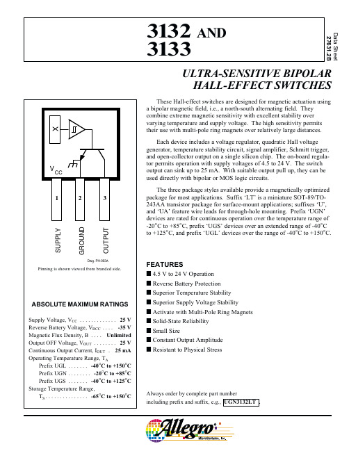
FEATURES I 4.5 V to 24 V Operation I Reverse Battery Protection I Superior Temperature Stability I Superior Supply Voltage Stability I Activate with Multi-Pole Ring Magnets I Solid-State Reliability I Small Size I Constant Output Amplitude I Resistant to Physical Stress
—
-20
—
52
—
NOTE: As used here, negative flux densities are defined as less than zero (algebraic convention.) Typical values are at TA = +25°C and VCC = 12 V.
Characteristic Operate Point
Release Point
Hysteresis
Symbol BOP
BRP
Bhys
Device Type* 3132 3133 3132 3133 Both
Min. — — -95 -75 30
Limits
康卡斯特机型

连铸机CONCAST——SBQ连铸的领先者Concast 提供的连续铸钢设备比业界中任何别的公司都多。
50多年来,Concast公司通过致力于连续铸钢的钢凝固工艺,向用户提供服务。
今天,采用Concast公司的设备已经成为电弧炉、二次冶炼设备和连铸的工业性能基准。
Concast公司致力于炼钢过程的开发,不管这种炼钢过程是使用废钢还是用铁矿石。
我们为长材产品部门的用户专门研究和开发冶炼、精炼和连铸工艺和技术,这是一个本公司竞争者都不能涉足的工作。
2 中间罐设计CONCAST中间罐设计有助于清除杂质,保证钢水流量稳定,并能使铸流之间的温度场均匀化。
通过模拟钢水流,可以优化中间罐的大小与形状以及挡板和挡墙的设计。
中间罐设计成能提供足够长的钢水停留时间(平均10分钟),这有助于清除杂质,使杂质有时间漂浮在表面,并被覆盖的粉末所吸收。
设计中间罐时考虑到了挡板、挡墙或紊流抑制剂,以使钢水流动分配最佳化,在钢水到达中间罐水口前消除冲击流产生的紊流。
这种设计有助于对结晶器钢水液面进行更好的控制,并使所有铸流中的钢水入口温度均匀化。
根据钢种、浇注时间和主要操作条件,针对各个工程项目选择分隔墙或紊流抑制剂的设计。
中间罐设计模型3 浸没式浇铸技术提供Concast 塞棒控制系统,用于浸没式浇铸。
Concast塞棒控制的特点:- 塞棒位置极其精确,控制迅速。
- 电机械系统可靠,维护需求低。
- 铸流启动顺序完成自动化。
使用Concast塞棒系统,使得对结晶器内钢水液面控制极佳,这对于有效润滑和实现良好表面质量极其重要。
用耐火材料管子进行浸没式浇铸,将钢水倒进结晶器中。
耐火材料管子能防止钢水流与环境(氧气和氮气)接触,并防止重新氧化造成杂质的形成。
在进行浸没式浇铸时,使用两种类型的耐火材料罩:- 浸没式入口水口(SEN)- 浸没式入口长水口(SES)采用SEN,防止钢流再次氧化的效果更好,因为喷嘴实际上布置做在中间罐的底部。
亚特诺新一代三相应用接触器产品介绍说明书
Motor control and protectionICON familyStart easily Protect preciselyIntroducing Eaton’s new contactor range for AC-3 applications to 170A. Perfectly suited for applications in the commercial and industrial segments for panel builders and machinery OEMs.The contactor has a smaller footprint than the existing xStart series and offers application adjusted ratings.Icon Contactors SeriesCoil voltages available are 24V50/60HZ, 110V50/60HZ, 230V50/60HZ, 400V50/60HZ, DC24V .Basic devices Rated operational current Max. motor rating for three-phase motors 50 - 60 Hz Conventional thermal current I th = I e AC-1at 40°C A Open Contact AC-3AC-3AC-4380 V 400 V I e220 V 230 V P 380 V 400 V P 660 V 690 V P 220 V 230 V P 380 V 400 V P 660 V 690 V P N/O = Normallyopened contact N/C = Normally 4 pole, 3 poleConnection type: Screw terminals9 2.5 4 4.5 1.5 2.5 3.6 20 – 1 N/C 12 3.5 5.5 6.5 2 3 4.4 20 1 N/O –12 3.5 5.5 6.5 2 3 4.4 20 – 1 N/C 15 4 7.5 7 2 3 4.4 20 1 N/O –154 7.5 7 2 3 4.4 20 – 1 N/C 3 poleConnection type: Screw terminals1857.511 2.5 4.56.5 401 N/O–18 5 7.511 2.5 4.5 6.5 40 – 1 N/C 257.51114 3.5 68.5 401 N/O–25 7.5 1114 3.5 6 8.5 40 – 1 N/C 32101515 4 710 451 N/O–32 10 1515 4 710 45 – 1 N/C 381118.515 4 710 451 N/O–3811 18.5 15 4 710 45 – 1 N/C 3 poleConnection type: Screw terminals40 12.5 18.523 5 912 60 1 N/O 1 N/C 50 15.5 2230 6 1014 80 1 N/O 1 N/C 65 20 3035 7 1217 98 1 N/O 1 N/C 7222 3735 7 1217 98 1 N/O 1 N/C 3 poleConnection type: Screw terminals80 25 3737112015110 1 N/O 1 N/C 95304545 1120151301 N/O1 N/C3 poleConnection type: Screw terminals115 37 5590 17 2843 160 ––150 48 75 96 20 3348 190 ––1705290140 20 3348 203––CMN00027DILM9-01N CMN00038DILM12-10N CMN00049DILM12-01N CMN00060DILM15-10N CMN00071DILM15-01N CMN00082DILM18-10N DILM18-01N CMN00104DILM25-10N DILM25-01N(CMN00126DILM32-10N DILM32-01N CMN00148DILM38-10N DILM38-01N CMN00170DILM40-11N DILM50-11N DILM65-11N DILM72-11N DILM80-11N DILM95-11N DILM115N DILM150N DILM170N (...)(...)(...)(...)(...)(...)(...)(...)(...)(...)(...)(...)(...)(...)(...)(...)(...)(...)(...)(...)(...)(...)• Phase failure sensitivity and temperature compensation • Reset pushbutton manual/auto • Test/off pushbutton• Auxiliary contact (1 N/O + 1 NC)•Fitted directly on the contactor of the maximum current to 175AIcon Overload relays ZB..N series0.1 – 0.16CMN00333CMN00335ZB12N-1,6CMN00336ZB12N-2,4CMN00337ZB12N-4CMN00338ZB12N-6CMN00339ZB12N-10CMN00340ZB12N-12CMN00341ZB12N-161 – 1.5CMN00352ZB32N-24CMN00353ZB32N-30CMN00354ZB32N-36CMN00355ZB32N-38CMN00356Setting range of overload releasesCircuit symbolAuxiliary contactFor use withI r AN/O = normally open contact N/C = normally closed contact0.4 – 0.6 1 N/O 1 N/C 0.6 – 1 1 N/O 1 N/C 1 – 1.6 1 N/O 1 N/C 1.6 – 2.4 1 N/O 1 N/C 2.4 – 4 1 N/O 1 N/C 4 – 6 1 N/O 1 N/C 6 – 10 1 N/O 1 N/C 9 – 12 1 N/O 1 N/C 12 –161 N/O1 N/C 17 – 24 1 N/O 1 N/C 22 – 30 1 N/O 1 N/C 29 – 36 1 N/O 1 N/C 33 – 381 N/O1 N/COverload relaysIcon Overloads ZB…N seriesSetting range of overload releasesCircuit symbolAuxiliary contactFor use withI r AN/O = normally open contact N/C = normally closed contact63 – 80 1 N/O 1 N/C 77 – 971 N/O1 N/C50 – 70 1 N/O 1 N/C 70 – 100 1 N/O 1 N/C 95 – 125 1 N/O 1 N/C 120 – 150 1 N/O 1 N/C 145 – 1751 N/O1 N/COverload relays Part no.Article no.– 25CMN00363– 50– 35– 25 – 50ZB95N-50 – 35ZB150N-35Icon Contactor Relays DILA…N seriesWiring method: Screw terminals Basic devices with interlocked opposing contacts ContactRated operational current AC – 15Conventional thermal current at 55°CN/O = Normally opened contact N/C = Normally closed contact220 V 230 V 240 V I e A380 V 400 V 415 V I e AI th A4 N/O – 4 416 3 N/O 1 N/C 4 4 16 2 N/O 2 N/C 4 4 16 1 N/O 3 N/C 4416–4 N/C4416DILA-40N DILA-31N DILA-22N DILA-13N DILA-04N(Coil voltages available are 24V50/60HZ, 110V50/60HZ, 230V50/60HZ, 400V50/60HZ, DC24V .• Varied 4-pole contact configurations • Conventional thermal current (Ith): 16A• Identical construction sizes for AC- and DC-operated contactor relays •Integrated surge suppressors for DC-operated contactor relaysA complete range of accessories are available for the Icon series, such as:• Auxiliary contacts (top mount)• Auxiliary contacts (side mount)• RC Suppressors• Varistor Suppressors• Pneumatic timer modules • Mechanical Interlocks • Sealable Shrouds•External Reset Button(...)(...)(...)(...)(...)E a t o n10 Kent RoadMascot NSW 2020Tel: 1300 332 866Fax: (02) 9693 1258Email: ************************ Eaton is a registered trademarkof Eaton Corporation.All trademarks are property of their respective owners.For more information about Eaton visit: Eaton’s mission is to improve the quality of life and the environment through the use of power management technologies and services. We provide sustainable solutions that help our customers effectively manage electrical, hydraulic, and mechanical power – more safely, more effi ciently, and more reliably. Eaton’s 2019 revenues were $21.4 billion, and we sell products to customers in more than 175 countries. We have approximately 95,000 employees.For more information about Eaton visit: 。
Amtech Tacky 助焊膏系列安全数据表说明书

Inventec Performance Chemicals USA, LLCSAFETY DATA SHEET (SDS)SECTION 1: PRODUCT AND COMPANY IDENTIFICATIONPRODUCT NAME: Amtech Tacky Paste Flux Series: 200, 400, 500, 600, 4000, SynTECH, WSFC-305L and #61 SYNONYMS:Tacky FluxMANUFACTURER: Inventec Performance Chemicals USA, LLCADDRESS:PO Box 989 Deep River, CT 06417 USAPHONE:860-526-8300FAX:860-526-8243EMERGENCY:Infotrac-(800)535-5035REVISION DATE:December 19, 2014REVISION DATE: 3DOCUMENT NAME:SDS-Tacky Flux-008PRODUCT USE:Bonding solder joints in production and repair of circuit boardsSECTION 2: HAZARDS IDENTIFICATIONCHEMICAL NAME:N/ACHEMICAL FAMILY:MixtureCHEMICAL FORMULA:N/AROUTES OF ENTRY: Inhalation, Ingestion, Skin/Eye ContactGHS:Signal Word: WarningHazard statement(s)H302 Harmful if swallowedH317 May cause an allergic skin reactionH320 Causes eye irritationH335 May cause respiratory irritationPrecautionary statement(s)P102 Keep out of reach of childrenP233 Keep container tightly closedP264 Wash hands thoroughly after handlingP270 Do not eat, drink or smoke when using this productP280 Wear protective gloves/protective clothing/eye protection/face protectionP302+P352 IF ON SKIN: Wash with plenty of soap and waterP305+P351 IF IN EYES: Rinse continuously with water for several minutesP404 Store in a closed containerP501 Dispose of contents/containers in accordance with Federal, State/Provincial, and/or local regulations POTENTIAL HEALTH EFFECTS:EYE CONTACT: May cause moderate irritation. Do not allow material to come in contact with eyes.SKIN CONTACT: May cause moderate skin irritation.INHALATION: May cause irritation to the respiratory tract.INGESTION: Harmful if swallowed. May cause irritation to the mouth, throat, and stomach. May cause abdominal discomfort, nausea, vomiting, and/or diarrhea.CHRONIC: Not established.SECTION 2 NOTES:Inventec Performance Chemicals USA, LLC does not recommend, manufacture, market, or endorse any of its products for human consumption.SECTION 3: COMPOSITION/INFORMATION ON INGREDIENTSIngredient CAS Number Exposure LimitsModified Rosins N/A N/APine Oil Derivatives 8000-41-7 N/AProprietary Ingredients N/A N/AMixed Carboxylic Acids N/A N/ASECTION 3 NOTES:Percentages of individual components are not listed as this information is considered a trade secret.SECTION 4: FIRST AID MEASURESEYES: Flush with plenty of water, contact a physician. If contact lenses can be removed easily, flush eyes without contact lenses. SKIN: Wash affected area with plenty of warm, soapy water. If irritation persists, seek medical attention.INGESTION: Call a physician or Poison Control Center immediately. Do not induce vomiting.INHALATION: Remove to fresh air. If not breathing, seek immediate medical attention.SECTION 5: FIRE-FIGHTING MEASURESEXTINGUISHING MEDIA: Dry chemical, foamSPECIAL FIRE FIGHTING PROCEDURES: Do not use water. Use NIOSH-approved self-contained Breathing Apparatusand full protective clothing if involved in a fire.UNUSUAL FIRE AND EXPLOSION HAZARDS:This product does not present any unusual fire and explosion hazards. SECTION 6: ACCIDENTAL RELEASE MEASURESACCIDENTAL RELEASE MEASURES: If material spills or leaks, collect and place into a properly labeled waste container. Remove traces of tacky flux using cloth rags or paper towels moistened with Isopropyl Alcohol. Follow on-site personal protective equipment recommendations.SECTION 6 NOTES:See Sections 2, 4, and 7 for additional information.SECTION 7: HANDLING AND STORAGEHANDLING/STORAGE: Keep containers tightly closed when not in use. Use care to avoid spills. Avoid inhalation of fumes or dust. Avoid contact with eyes, skin, and clothing.OTHER PRECAUTIONS: Empty containers may retain product residues in vapor, liquid, and/or solid form. All labeled hazard precautions should be observed.WORK HYGIENIC PRACTICES: Cosmetics/Food/Drink/Tobacco should not be consumed or used in work areas. Always wash hands after handling material and before applying or using cosmetics/food/drink/tobacco.SECTION 7 NOTES:For industrial use only.SECTION 8: EXPOSURE CONTROLS/PERSONAL PROTECTIONVENTILATION: Provide sufficient mechanical (general and/or local exhaust) ventilation to maintain exposure below TLVs. RESPIRATORY PROTECTION: Use with adequate ventilation.EYE PROTECTION: Use with appropriate safety glasses.SKIN PROTECTION: Protective gloves and clothing should be worn when handling material. Wash hands thoroughly with soap and water upon leaving the work area.SECTION 9: PHYSICAL AND CHEMICAL PROPERTIESAPPEARANCE: Clear, White, or Yellow to Dark Amber gelODOR: Mild odorODOR THRESHOLD: Not establishedpH as SUPPLIED: N/ASECTION 9: PHYSICAL AND CHEMICAL PROPERTIES (continued)MELTING POINT: Not establishedFREEZING POINT: Not establishedINITIAL BOILING POINT: Not establishedBOILING RANGE: Not establishedFLASH POINT: Not establishedEVAPORATION RATE: Not establishedFLAMMABILITY (solid): Not establishedUPPER/LOWER FLAMMABILITY: Not establishedUPPER/LOWER EXPLOSIVE LIMITS:Not establishedVAPOR PRESSURE (mmHg): N/A (°F/°C)VAPOR DENSITY (AIR = 1): N/A (°F/°C)RELATIVE DENSITY: Not establishedSOLUBILITY IN WATER: PartiallyPARTITION COEFFICIENT (n-octanol/water): Not establishedAUTOIGNITION TEMPERATURE: Not establishedDECOMPOSITION TEMPERATURE: Not establishedVISCOSITY: N/A (°F/°C)SECTION 10: STABILITY AND REACTIVITYSTABILITY: StableCONDITIONS TO AVOID (STABILITY): Freezing temperatures. High temperatures. INCOMPATIBILITY (MATERIAL TO AVOID): Strong oxidizing materialsHAZARDOUS DECOMPOSITION/BY-PRODUCTS: Harmful organic fumes and toxic oxide fumes may form at elevatedtemperatures.POSSIBILITY OF HAZARDOUS REACTIONS: Will not occurSECTION 11: TOXICOLOGICAL INFORMATIONACUTE TOXICITY: Not availableSKIN CORRISION/IRRITATION: Not establishedSERIOUS EYE DAMAGE/IRRITATION: Not availableRESPIRATORY OR SKIN SENSITIZATION: Not establishedGERM CELL MUTAGENICITY: Not availableCARCINOGENICITY: Not availableREPRODUCTIVE TOXICITY: Not availableSTOT-SINGLE EXPOSURE: Not availableSTOT-REPEATED EXPOSURE: Not availableASPIRATION HAZARD: Not availableSECTION 12: ECOLOGICAL INFORMATIONTOXICITY: Product not testedPERSISTENCE AND DEGRADIBILITY: Product not testedBIOACCUMULATIVE POTENTIAL: Product not testedMOBILITY IN SOIL: Product not testedOTHER ADVERSE EFFECTS: Product not testedSECTION 13: DISPOSAL CONSIDERATIONSWASTE DISPOSAL METHOD: Scrap and waste solder should be stored in a dry, sealed container for later disposal. Disposal must be in accordance with Federal, State/Provincial, and Local Regulations.SECTION 14: TRANSPORT INFORMATIONTransport in accordance with applicable regulations and requirements.UN Number: Not availableUN Proper Shipping Name: Not availablePackaging Group:Not applicableEnvironmental Hazards:NoneTRANSPORT HAZARD CLASSES:US DOT Hazardous Material Classification: Tacky Flux is not listed as a DOT hazardous materialWater Transportation: Tacky Flux is not listed as a hazardous materialIATA Hazardous Material Classification: Tacky Flux is not listed as IATA hazardous materialSECTION 15: REGULATORY INFORMATIONAll ingredients used to manufacture this product are listed on the EPA TSCA Inventory.U.S. FEDERAL REGULATIONS: Not regulatedSTATE REGULATIONS: Not regulatedINTERNATIONAL REGULATIONS: Not regulatedSECTION 16: OTHER INFORMATIONHMIS Rating: Health=1 Flammability=1 Physical Hazard=0 Personal Protection=X KEY:N/A: Not applicableGHS: Global Harmonized SystemOSHA: Occupational Safety and Health AdministrationACGIH: American Conference of Governmental Industrial HygienistsNTP: National Toxicology ProgramIARC: International Agency for Research on CancerCAS: Chemical Abstract ServiceNIOSH: National Institute for Occupational Safety & HealthSTOT: Specific target organ toxicityTLV: Threshold limit valueUS DOT: United States Department of TransportationDOT: Department of TransportationIATA: International Air Transport AssociationEPA:Environmental Protection AgencyTSCA:Toxic Substance Control ActHMIS:Hazardous Material Identification SystemPREPARATION INFORMATION:This update supersedes all previously released documents.PREPARED BY: Wendy W. GesickAPPROVED BY: Leigh W. GesickDISCLAIMER:The information contained herein is based on data considered to be accurate but does not purport to be all-inclusive and shall be used only as a guide. No warranty is expressed or implied regarding the accuracy of this data and Inventec Performance Chemicals USA, LLC shall not be held liable for any damage resulting from any handling or contact with the above product. Liability is expressly disclaimed for loss or injury arising out of use of this information or the use of any materials designated. This material is not for resale, unauthorized distribution, or personal use.。
碳氢氧元素分析仪器

碳氢氧元素分析仪器碳氢元素分析仪,碳氢氧分析仪器等主要技术指标:碳氢氧元素分析仪是高准确度、高灵敏度的有机高分子电化学传感器。
采用先进的单片微机控制技术和测量芯片,可以直接测出土壤样品中有效态含量。
该产品不仅适用于工业场所环境的检测,也可作为一般实验室用的废水污染物总量检测。
产品符合GB/ T18456-1997的要求。
其技术指标均达到或优于国际同类产品水平,具有非常广阔的市场前景。
产品符合《固体废弃物试验方法》( GB/ T30378.1)。
由上海航空电源研究所提供,实现了智能化操作及系统管理。
自动采集数据,并对测量数据进行处理、计算、打印;软件界面友好、易操作、维护简便。
该产品整套设备从材料采购至出厂调试,各个环节严格按照质量保证体系要求进行,充分体现出生产过程中的严肃性、科学性与规范性。
本公司承诺:严把质量关,做到“人无我有,人有我优”。
碳氢元素分析仪测试快速简单,广泛应用于各种实验室或企事业单位。
可在较短的时间内为您的试验结果作出正确判断!碳氢元素分析仪的作用就是能够监测某些矿石、土壤、沙尘、淤泥、石油化工废液以及残渣排放中的碳氢元素含量的一种分析仪器。
主要用途是确认化工排泄物是否被小型金属或者矿藏所吸收或存留,从而达成防止地下水污染的目的。
碳氢元素分析仪的特点是快速检测、简易、准确度高、使用寿命长、无二次污染等优点。
在分析时,将待测土壤浸入盛有指示剂的锥形瓶里(指示剂采用硼酸钠溶液),盖紧塞子,向锥形瓶内加入少许已知浓度的硼酸钠溶液,摇匀,然后用标准曲线法,直接测得样品溶液的吸光度值。
最后再换算出土壤中碳氢元素的含量。
可根据用户需要配备上位机( PC 机),实现对碳氢元素含量的计算、显示、储存、打印等功能。
还可以通过专门开发的分析软件对样品数据进行分析,并且对所获取的结果可以用 EXCEL、 WORD、 EXCBWER 等文档进行保存,然后打印输出。
碳氢元素分析仪具有很多突出的优势。
在目前我们对环境监测手段仍停留在快速监测阶段的情况下,碳氢元素分析仪因为其优异的特性受到了越来越多的青睐,被越来越多的用户所接受。
FISHER角阀高压阀 中英文对照表
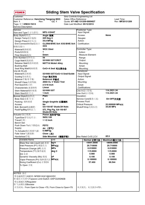
Item: 1 Rev: Qty: 1 Quote: 871-MZ-131209-0009627 Rev: MF20131209 Tags: 位号05ESV-5413 Date Last Modified: 09/12/2013Service Description:Service: Positioner Type:Size and Type尺寸与型号: NPS 4 EHAT Input Signal:Body Style阀形式: Angle 角阀 Access: NoneDesign Temp设计温度: 205 Deg C Gauges:Design Press设计压力: 34.8 MPag Action:End Connect/In/Out进出口磅级及接口: CL2500/BWE Sch XXS/BWE SchXXSCertification:Material阀体材质: WCC Steel Controller Type:Ports阀喉数量: 1 Action:Flow Directn流向: Down Measure Element:Trim Number内件代号: 54 Range:Cage Matl阀笼材质: S31600 SST/CRCT Output:Retainer Matl保持环材质: N07718 Nickel Alloy Mounting:Bushing Matl: Airset:Seat Ring Matl阀座材质: CoCr-A Seat 司太莱合金 Mounting:VALVE PLUG Transducer: Material阀芯材质: S31600 SST/CoCr-A Seat/Guide Input Signal:Guiding导向形式: Cage 笼式导向 Output Signal:Balance平衡/非平衡: Balanced 平衡式 Action:Shutoff Class关闭等级: ANSI CL V Water Test Mounting:Port Size阀喉口径: 2 5/16 Inch Airset:Characteristic:流量特性Linear Certifications:Stem Material阀杆材质: S31600 SST Line In进口管线: 114.3X21.34Stem Size阀杆尺寸: 1 Inch Line Out出口管线: 114.3X21.34 Bonnet Style阀盖形式: Plain Insulation:Boss Size支架尺寸: 5 Service Cond服务工况: On-OFF开关型Packing: 填料材质Single Graphite 石墨填料Process Fluid:Access: No Critical Pressure: 22.000000 MPa(a) Bolt, Bonnet阀盖螺栓: SA-193-B7 Studs/2H Nuts Shutoff Drop关闭压差: 34.80 MPaPackFlg/Bltg填料法兰: STL Pkg Flg, SA-193-B7Studs/2H NutsActuator:执行机构Piston 双作用气缸Type/Size型号民/尺寸: 585C/100Travel行程 : 1 1/2 InchBench Set:Push Down To向下推趋向: PDTCSupply: Air (空气)To Actuator执行机构气源: 0.4MPagFails Valve气源故障: Close(关)Handwheel手轮: Side Mounted (侧装手轮)Max Rated Cv额定CV: 85.9 Variable Name Unit Normal 正常工况Maximum最大工况Mass flow rate Liquid (wl) 流量kg/h 15551.0000 18000.0000Inlet Pressure (P1) 阀前压力MPa(g) 29.710000 29.710000Pressure Change (dP) 压差MPa 0.010000 0.010000Temperature (T1) 操作温度deg C 115.0000 115.0000SG 比重0.980 0.980Dynamic Viscosity (Mu) 粘度cP 0.100 0.100Vapor Pressure (Pv) 饱和蒸汽压MPa(a) 0.100000 0.100000Sizing Coefficient (Cv) 计算CV 57.490 66.544% Open 开度NOTES: 备注带电磁阀型号ASCO: NF8551A321@24VDC带限位开关型号Topworx Limit Switch: DXP-E20GNEB带过滤减压阀Regulator带气动增压器Booster开关时间:From Open to Close <7S, From Close to Open<7S 从开到关,从关到开<7秒。
- 1、下载文档前请自行甄别文档内容的完整性,平台不提供额外的编辑、内容补充、找答案等附加服务。
- 2、"仅部分预览"的文档,不可在线预览部分如存在完整性等问题,可反馈申请退款(可完整预览的文档不适用该条件!)。
- 3、如文档侵犯您的权益,请联系客服反馈,我们会尽快为您处理(人工客服工作时间:9:00-18:30)。
SIPMOS® Power Transistor• N channel• Enhancement mode• Avalanche-ratedType V DS I D R DS(on)Package Ordering Code BUZ 344100 V50 A0.035 ΩTO-218 AA C67078-S3132-A2Maximum RatingsParameter Symbol Values UnitContinuous drain current T C = 25 °C I D50APulsed drain current T C = 25 °C I Dpuls200Avalanche current,limited by T jmax I AR 50Avalanche energy,periodic limited by T jmax E AR 18.5mJAvalanche energy, single pulseI D = 50 A, V DD = 25 V, R GS = 25 ΩL = 240 µH, T j = 25 °C E AS400Gate source voltage V GS± 20VPower dissipation T C = 25 °C P tot170WOperating temperature T j -55 ... + 150°C Storage temperature T stg -55 ... + 150 Thermal resistance, chip case R thJC ≤ 0.74K/W Thermal resistance, chip to ambient R thJA 75DIN humidity category, DIN 40 040 EIEC climatic category, DIN IEC 68-1 55 / 150 / 56Electrical Characteristics, at T j = 25°C, unless otherwise specifiedParameter Symbol Values Unitmin.typ.max.Static CharacteristicsDrain- source breakdown voltage V GS = 0 V, I D = 0.25 mA, T j = 25 °C V(BR)DSS100--VGate threshold voltage V GS=V DS, I D = 1 mA V GS(th)2.1 3 4Zero gate voltage drain currentV DS = 100 V, V GS = 0 V, T j = 25 °C V DS = 100 V, V GS = 0 V, T j = 125 °C I DSS--100.11001µAGate-source leakage current V GS = 20 V, V DS = 0 V I GSS- 10 100nADrain-Source on-resistance V GS = 10 V, I D = 32 A R DS(on)- 0.03 0.035ΩElectrical Characteristics, at T j = 25°C, unless otherwise specifiedParameter Symbol Values Unitmin.typ.max. Dynamic CharacteristicsTransconductanceV DS≥ 2 *I D * R DS(on)max, I D = 32 A g fs15 28-SInput capacitanceV GS = 0 V, V DS = 25 V, f = 1 MHz C iss- 2400 3200pFOutput capacitanceV GS = 0 V, V DS = 25 V, f = 1 MHz C oss- 730 1100Reverse transfer capacitanceV GS = 0 V, V DS = 25 V, f = 1 MHz C rss- 430 650Turn-on delay timeV DD = 30 V, V GS = 10 V, I D = 3 A R GS = 50 Ωt d(on)- 33 50nsRise timeV DD = 30 V, V GS = 10 V, I D = 3 A R GS = 50 Ωt r- 140 210Turn-off delay timeV DD = 30 V, V GS = 10 V, I D = 3 A R GS = 50 Ωt d(off)- 500 670Fall timeV DD = 30 V, V GS = 10 V, I D = 3 A R GS = 50 Ωt f- 230 310Electrical Characteristics, at T j = 25°C, unless otherwise specifiedParameter Symbol Values Unitmin.typ.max. Reverse DiodeInverse diode continuous forward current T C = 25 °C I S-- 50AInverse diode direct current,pulsed T C = 25 °C I SM-- 200Inverse diode forward voltage V GS = 0 V, I F = 100 A V SD- 1.6 1.8VReverse recovery timeV R = 30 V, I F=l S, d i F/d t = 100 A/µs t rr- 170-nsReverse recovery chargeV R = 30 V, I F=l S, d i F/d t = 100 A/µs Q rr- 0.9-µCDrain current I D = ƒ(T C )parameter: V GS ≥ 10 V20406080100120°C160T C0 5 10 1520 25 30 35 40 45 A55 IDPower dissipation P tot = ƒ(T C )20406080100120°C 160T C0 20 40 6080 100 120 140 W180 P totSafe operating area I D = ƒ(V DS )parameter: D = 0.01, T C = 25°C10 10 10 10 I D101010V V DS Transient thermal impedance Z th JC = ƒ(t p )parameter: D = t p / T10 10 10 10 Z thJC10101010101010 10s t pTyp. output characteristics I D = ƒ(V DS )parameter: t p = 80 µs0.01.02.03.04.05.06.0V8.0V DSI DTyp. drain-source on-resistance R DS (on) = ƒ(I D )parameter: V GS20406080A 110I DR DS (on)Typ. transfer characteristics I D = f (V GS )parameter: t p = 80 µs V DS ≥2 x I D x R DS(on)max12345678V 10V GS0 5 10 15 20 25 30 35 40 45 50 55 60 65A 75 I DTyp. forward transconductance g fs = f (I D )parameter: t p = 80 µs,V DS ≥2 x I D x R DS(on)max1020304050A 70I D0 4 8 12 16 20 24 28 S34 g fsGate threshold voltageV GS (th) = ƒ(T j)parameter: V GS = V DS, I D = 1 mAVGS(th)-60-202060100°C160Tj Drain-source on-resistanceR DS (on) = ƒ(T j)parameter: I D = 32 A, V GS = 10 V-60-202060100°C160TjRDS (on)Typ. capacitancesC = f (V DS)parameter:V GS = 0V, f = 1MHz0510********V40VDS10101010CForward characteristics of reverse diodeI F = ƒ(V SD)parameter: T j, t p = 80 µs10101010IF0.00.40.8 1.2 1.6 2.0 2.4V 3.0VSDAvalanche energy E AS = ƒ(T j )parameter: I D = 50 A, V DD = 25 V R GS = 25 Ω, L = 240 µH20406080100120°C 160T j0 50 100 150 200250300350 mJ450 EASTyp. gate charge V GS = ƒ(Q Gate )parameter: I D puls = 75 A4080120160200240280320nC 380Q GateV GSDrain-source breakdown voltage V (BR)DSS = ƒ(T j )-60-202060100°C 160T j90 9294 96 98 100 102 104 106 108 110 112 114116V 120 V (BR)DSS。