MEMORY存储芯片MAX3490ECSA+T中文规格书
MEMORY存储芯片MAX488ESA+T中文规格书

OUTPUT CURRENT vs. RECEIVER OUTPUT HIGH VOLTAGE
-25
-20
-15
-10
-5
0 1.5 2.0 2.5 3.0 3.5 4.0 4.5 5.0 OUTPUT HIGH VOLTAGE (V)
RECEIVER OUTPUT HIGH VOLTAGE vs. TEMPERATURE
DE
low.
If
the
inputs
are
in
this
state
for
less than 50ns, the parts are guaranteed not to enter shutdown. If the inputs are in this state for at least 600ns, the parts are
0.9
0.8 IRO = 8mA
0.7
0.6
0.5
0.4
0.3
0.2
0.1
0 -60 -40 -20 0 20 40 60
TEMPERATURE (°C)
80 100
MAX481E-04
OUTPUT CURRENT (mA)
DRIVER OUTPUT CURRENT vs. DIFFERENTIAL OUTPUT VOLTAGE
Note 2: All typical specifications are given for VCC = 5V and TA = +25°C.
Note 3: Supply current specification is valid for loaded transmitters when DE = 0V.
MEMORY存储芯片MAX13487EESA+T中文规格书

Half-Duplex RS-485-/RS-422-Compatible Transceiver with AutoDirection Control MAX13487E/MAX13488E General DescriptionThe MAX13487E/MAX13488E +5V, half-duplex, ±15kV ESD-protected RS-485/RS-422-compatible transceivers feature one driver and one receiver. The MAX13487E/MAX13488E include a hot-swap capability to eliminate false transitions on the bus during power-up or live insertion.The MAX13487E/MAX13488E feature Maxim’s propri-etary AutoDirection control. This architecture makes the devices ideal for applications, such as isolated RS-485 ports, where the driver input is used in conjunction with the driver-enable signal to drive the differential bus.The MAX13487E features reduced slew-rate drivers that minimize EMI and reduce reflections caused by improperly terminated cables, allowing error-free trans-mission up to 500kbps. The MAX13488E driver slew rate is not limited, allowing transmit speeds up to 16Mbps.The MAX13487E/MAX13488E feature a 1/4-unit load receiver input impedance, allowing up to 128 trans-ceivers on the bus. These devices are intended for half-duplex communications. All driver outputs are protected to ±15kV ESD using the Human Body Model. The MAX13487E/MAX13488E are available in an 8-pin SO package. The devices operate over the extended -40°C to +85°C temperature range.Applications Isolated RS-485 InterfacesUtility MetersIndustrial ControlsIndustrial Motor DrivesAutomated HVAC SystemsBenefits and Features •AutoDirection Saves Space and BOM Cost •AutoDirection Enables Driver Automatically on Transmission, Eliminating an Opto or Other Discrete Means of Isolation •8-Pin SO Package •Robust Protection Features for Telecom, Industrial,and Isolated Applications •Hot-Swap Capability to Eliminate False Transitions on the Bus During Power-Up or Live Insertion •Extended ESD Protection for RS-485 I/O Pins (±15kV Human Body Model)•Options Optimize Designs for Speed or Errorless Data Transmission •Enhanced Slew-Rate Limiting Facilitates Error-Free Data Transmission (MAX13487E)•High-Speed Version (MAX13488E) Allows for Transmission Speeds Up to 16Mbps •1/4-Unit Load, Allowing Up to 128 Transceivers on the Bus Ordering Information/Selector Guide+Note:All devices operate over the -40°C to +85°C temperature range.Pin Configuration/Typical Application Circuit appear at end of data sheet.Functional Diagram 19-0740; Rev 1; 2/15找MEMORY 、二三极管上美光存储MAX13487E/MAX13488E Half-Duplex RS-485-/RS-422-Compatible Transceiver with AutoDirection Control Integrated | 7Typical Operating Characteristics (continued)(V CC = +5.0V, T A = +25°C, unless otherwise noted.)RECEIVER PROPAGATION vs. TEMPERATURE(MAX13488E)TEMPERATURE (°C)R E C E I VE R P R O P A G A T I O N (n s )603510-1510203040-4085DRIVER PROPAGATION (500kbps)(MAX13487E)M A X 13487E t o c 17DI 2V/div A-B5V/div400ns/div DRIVER PROPAGATION (16Mbps)(MAX13488E)DI 2V/div A-B 5V/div 10ns/div RECEIVER PROPAGATION (16Mbps)(MAX13488E)MA X 13487E t o c 19B 2V/div RO 2V/div A2V/div10ns/div DRIVING 16nF (19.2kbps)(MAX13487E)M A X 13487E t o c 20DI2V/divA-B 5V/div10μs/div DRIVING 16nF (19.2kbps)(MAX13488E)M A X 13487E t o c 21DI2V/div A-B5V/div 10μs/div DRIVING 16nF (750kbps)(MAX13488E)M A X 13487E t o c 22DI 2V/div A-B 5V/div400ns/div。
MEMORY存储芯片MAX1487ECSA+T中文规格书

For pricing, delivery, and ordering information, please contact Maxim Direct at 1-888-629-4642, or visit Maxim’s website at General DescriptionThe MAX481E, MAX483E, MAX485E, MAX487E–MAX491E, and MAX1487E are low-power transceivers forRS-485 and RS-422 communications in harsh environ-ments. Each driver output and receiver input is protectedagainst ±15kV electro-static discharge (ESD) shocks,without latchup. These parts contain one driver and onereceiver. The MAX483E, MAX487E, MAX488E, andMAX489E feature reduced slew-rate drivers that minimizeEMI and reduce reflections caused by improperly termi-nated cables, thus allowing error-free data transmissionup to 250kbps. The driver slew rates of the MAX481E,MAX485E, MAX490E, MAX491E, and MAX1487E are notlimited, allowing them to transmit up to 2.5Mbps.These transceivers draw as little as 120µA supply cur-rent when unloaded or when fully loaded with disableddrivers (see Selector Guide ). Additionally, the MAX481E,MAX483E, and MAX487E have a low-current shutdownmode in which they consume only 0.5µA. All parts oper-ate from a single +5V supply.Drivers are short-circuit current limited, and are protectedagainst excessive power dissipation by thermal shutdowncircuitry that places their outputs into a high-impedancestate. The receiver input has a fail-safe feature that guar-antees a logic-high output if the input is open circuit.The MAX487E and MAX1487E feature quarter-unit-loadreceiver input impedance, allowing up to 128 trans-ceivers on the bus. The MAX488E–MAX491E aredesigned for full-duplex communications, while theMAX481E, MAX483E, MAX485E, MAX487E, andMAX1487E are designed for half-duplex applications.For applications that are not ESD sensitive see the pin-and function-compatible MAX481, MAX483, MAX485,MAX487–MAX491, and MAX1487.ApplicationsLow-Power RS-485 TransceiversLow-Power RS-422 TransceiversLevel TranslatorsTransceivers for EMI-Sensitive Applications Industrial-Control Local Area Networks Next-Generation Device Features ♦For Fault-Tolerant Applications:MAX3430: ±80V Fault-Protected, Fail-Safe, 1/4-Unit Load, +3.3V, RS-485 Transceiver MAX3080–MAX3089: Fail-Safe, High-Speed (10Mbps), Slew-Rate-Limited, RS-485/RS-422Transceivers ♦For Space-Constrained Applications:MAX3460–MAX3464: +5V, Fail-Safe, 20Mbps,Profibus, RS-485/RS-422 Transceivers MAX3362: +3.3V, High-Speed, RS-485/RS-422Transceiver in a SOT23 Package MAX3280E–MAX3284E: ±15kV ESD-Protected,52Mbps, +3V to +5.5V, SOT23, RS-485/RS-422True Fail-Safe Receivers MAX3030E–MAX3033E: ±15kV ESD-Protected,+3.3V, Quad RS-422 Transmitters ♦For Multiple Transceiver Applications:MAX3293/MAX3294/MAX3295: 20Mbps, +3.3V,SOT23, RS-485/RS-422 Transmitters ♦For Fail-Safe Applications:MAX3440E–MAX3444E: ±15kV ESD-Protected,±60V Fault-Protected, 10Mbps, Fail-Safe RS-485/J1708 Transceivers ♦For Low-Voltage Applications:MAX3483E/MAX3485E/MAX3486E/MAX3488E/MAX3490E/MAX3491E: +3.3V Powered, ±15kV ESD-Protected, 12Mbps, Slew-Rate-Limited,True RS-485/RS-422 TransceiversOrdering InformationOrdering Information continued at end of data sheet.Selector Guide appears at end of data sheet .19-0410; Rev 4; 10/03找MEMORY 、二三极管上美光存储±15kV ESD-Protected, Slew-Rate-Limited,Low-Power, RS-485/RS-422 TransceiversFigure 6. IEC1000-4-2 ESD Test ModelFigure 8. Driver DC Test LoadFigure 7. IEC1000-4-2 ESD Generator Current WaveformFigure 9. Receiver Timing Test Load Figure 4. Human Body ESD Test ModelFigure 5. Human Body Model Current Waveform MAX481E/MAX483E/MAX485E/MAX487E–MAX491E/MAX1487E10 Integrated。
MEMORY存储芯片MAX660ESA+T中文规格书

MAX660 CMOS Monolithic Voltage ConverterM A X 660CMOS Monolithic Voltage Converter ______________Detailed DescriptionThe MAX660 capacitive charge-pump circuit eitherinverts or doubles the input voltage (see TypicalOperating Circuits ). For highest performance, loweffective series resistance (ESR) capacitors should beused. See Capacitor Selection section for more details.When using the inverting mode with a supply voltageless than 3V, LV must be connected to G ND. Thisbypasses the internal regulator circuitry and providesbest performance in low-voltage applications. Whenusing the inverter mode with a supply voltage above3V, LV may be connected to GND or left open. The partis typically operated with LV grounded, but since LVmay be left open, the substitution of the MAX660 for theICL7660 is simplified. LV must be grounded when over-driving OSC (see Changing Oscillator Frequency sec-tion). Connect LV to OUT (for any supply voltage) whenusing the doubling mode.__________Applications InformationNegative Voltage ConverterThe most common application of the MAX660 is as acharge-pump voltage inverter. The operating circuituses only two external capacitors, C1 and C2 (seeTypical Operating Circuits ).Even though its output is not actively regulated, theMAX660 is very insensitive to load current changes. Atypical output source resistance of 6.5Ωmeans thatwith an input of +5V the output voltage is -5V underlight load, and decreases only to -4.35V with a load of100mA. Output source resistance vs. temperature andsupply voltage are shown in the T ypical OperatingCharacteristics graphs.Output ripple voltage is calculated by noting the outputcurrent supplied is solely from capacitor C2 during one-half of the charge-pump cycle. This introduces a peak-to-peak ripple of:V RIPPLE = I OUT +I OUT (ESR C2)2(f PUMP ) (C2)For a nominal f PUMP of 5kHz (one-half the nominal 10kHz oscillator frequency) and C2 = 150µF with an ESR of 0.2Ω, ripple is approximately 90mV with a 100mA load current. If C2 is raised to 390µF, the ripple drops to 45mV.Positive Voltage Doubler The MAX660 operates in the voltage-doubling mode as shown in the T ypical Operating Circuit.The no-load output is 2 x V IN .Other Switched-Capacitor Converters Please refer to Table 1, which shows Maxim’s charge-pump offerings.Changing Oscillator Frequency Four modes control the MAX660’s clock frequency, as listed below:FC OSC Oscillator Frequency Open Open 10kHz FC = V+Open 80kHz Open or External See Typical Operating FC = V+Capacitor Characteristics Open External External Clock Frequency Clock When FC and OSC are unconnected (open), the oscil-lator runs at 10kHz typically. When FC is connected to V+, the charge and discharge current at OSC changes from 1.0µA to 8.0µA, thus increasing the oscillatorTable 1. Single-Output Charge Pumps。
MEMORY存储芯片MAX490CPA+中文规格书
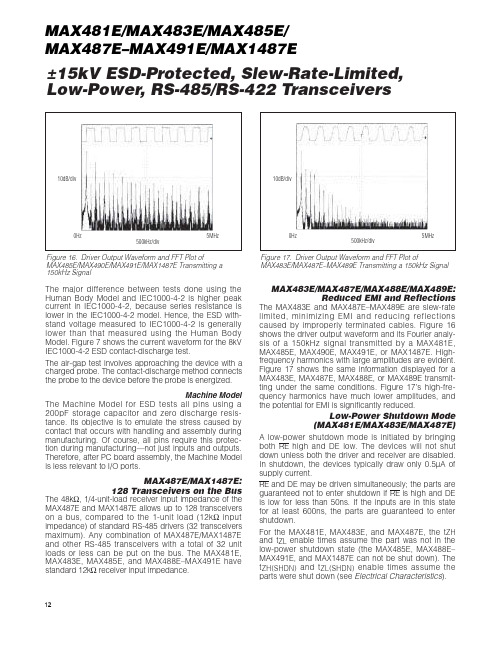
±15kV ESD-Protected, Slew-Rate-Limited, Low-Power, RS-485/RS-422 TransceiversThe major difference between tests done using the Human Body Model and IEC1000-4-2 is higher peak current in IEC1000-4-2, because series resistance is lower in the IEC1000-4-2 model. Hence, the ESD with-stand voltage measured to IEC1000-4-2 is generally lower than that measured using the Human Body Model. Figure 7 shows the current waveform for the 8kV IEC1000-4-2 ESD contact-discharge test.The air-gap test involves approaching the device with a charged probe. The contact-discharge method connects the probe to the device before the probe is energized.Machine Model The Machine Model for ESD tests all pins using a 200pF storage capacitor and zero discharge resis-tance. Its objective is to emulate the stress caused by contact that occurs with handling and assembly during manufacturing. Of course, all pins require this protec-tion during manufacturing—not just inputs and outputs. Therefore,after PC board assembly,the Machine Model is less relevant to I/O ports.MAX487E/MAX1487E:128 Transceivers on the Bus The 48kΩ, 1/4-unit-load receiver input impedance of the MAX487E and MAX1487E allows up to 128 transceivers on a bus, compared to the 1-unit load (12kΩinput impedance) of standard RS-485 drivers (32 transceivers maximum). Any combination of MAX487E/MAX1487E and other RS-485 transceivers with a total of 32 unit loads or less can be put on the bus. The MAX481E, MAX483E, MAX485E, and MAX488E–MAX491E have standard 12kΩreceiver input impedance.MAX483E/MAX487E/MAX488E/MAX489E:Reduced EMI and Reflections The MAX483E and MAX487E–MAX489E are slew-rate limited, minimizing EMI and reducing reflections caused by improperly terminated cables. F igure 16 shows the driver output waveform and its Fourier analy-sis of a 150kHz signal transmitted by a MAX481E, MAX485E, MAX490E, MAX491E, or MAX1487E. High-frequency harmonics with large amplitudes are evident.F igure 17 shows the same information displayed for a MAX483E, MAX487E, MAX488E, or MAX489E transmit-ting under the same conditions. F igure 17’s high-fre-quency harmonics have much lower amplitudes, and the potential for EMI is significantly reduced.Low-Power Shutdown Mode(MAX481E/MAX483E/MAX487E) A low-power shutdown mode is initiated by bringing both RE high and DE low. The devices will not shut down unless both the driver and receiver are disabled. In shutdown, the devices typically draw only 0.5µA of supply current.RE and DE may be driven simultaneously; the parts are guaranteed not to enter shutdown if RE is high and DE is low for less than 50ns. If the inputs are in this state for at least 600ns, the parts are guaranteed to enter shutdown.F or the MAX481E, MAX483E, and MAX487E, the t ZH and t ZL enable times assume the part was not in the low-power shutdown state (the MAX485E, MAX488E–MAX491E, and MAX1487E can not be shut down). The t ZH(SHDN)and t ZL(SHDN)enable times assume the parts were shut down (see Electrical Characteristics).Figure 16. Driver Output Waveform and FFT Plot of MAX485E/MAX490E/MAX491E/MAX1487E Transmitting a 150kHz SignalFigure 17. Driver Output Waveform and FFT Plot ofMAX483E/MAX487E–MAX489E Transmitting a 150kHz SignalMAX481E/MAX483E/MAX485E/ MAX487E–MAX491E/MAX1487E 12±15kV ESD-Protected, Slew-Rate-Limited, Low-Power, RS-485/RS-422 TransceiversOrdering Information (continued)Selector GuideChip InformationTRANSISTOR COUNT: 295MAX481E/MAX483E/MAX485E/MAX487E–MAX491E/MAX1487E。
MEMORY存储芯片MAX490EESA+T中文规格书

Ir
PEAK-TO-PEAK RINGING
(NOT DRAWN TO SCALE)
TIME
tDL CURRENT WAVEFORM
Figure 5. Human Body Model Current Waveform
I 100% 90%
IPEAK
DEVICE UNDER TEST
10%
tr = 0.7ns to 1ns
2
—
3
–R—E–
Receiver Output Enable. RO is enabled when –R—E– is low; RO is high impedance when R–—E– is high.
Driver Output Enable. The driver outputs, Y and Z, are
enabled by bringing DE high. They are high imped-
3
—
4
DE
ance when DE is low. If the driver outputs are enabled,
the parts function as line drivers. While they are high impedance, they function as line receivers if –R—E– is low.
—
—
B
Inverting Receiver Input and Inverting Driver Output
—
7
11
B
Inverting Receiver Input
8
1
14
VCC
MEMORY存储芯片MAX13487EESA+T中文规格书
Half-Duplex RS-485-/RS-422-Compatible Transceiver with AutoDirection Control MAX13487E/MAX13488E General DescriptionThe MAX13487E/MAX13488E +5V, half-duplex, ±15kV ESD-protected RS-485/RS-422-compatible transceivers feature one driver and one receiver. The MAX13487E/MAX13488E include a hot-swap capability to eliminate false transitions on the bus during power-up or live insertion.The MAX13487E/MAX13488E feature Maxim’s propri-etary AutoDirection control. This architecture makes the devices ideal for applications, such as isolated RS-485 ports, where the driver input is used in conjunction with the driver-enable signal to drive the differential bus.The MAX13487E features reduced slew-rate drivers that minimize EMI and reduce reflections caused by improperly terminated cables, allowing error-free trans-mission up to 500kbps. The MAX13488E driver slew rate is not limited, allowing transmit speeds up to 16Mbps.The MAX13487E/MAX13488E feature a 1/4-unit load receiver input impedance, allowing up to 128 trans-ceivers on the bus. These devices are intended for half-duplex communications. All driver outputs are protected to ±15kV ESD using the Human Body Model. The MAX13487E/MAX13488E are available in an 8-pin SO package. The devices operate over the extended -40°C to +85°C temperature range.Applications Isolated RS-485 InterfacesUtility MetersIndustrial ControlsIndustrial Motor DrivesAutomated HVAC SystemsBenefits and Features •AutoDirection Saves Space and BOM Cost •AutoDirection Enables Driver Automatically on Transmission, Eliminating an Opto or Other Discrete Means of Isolation •8-Pin SO Package •Robust Protection Features for Telecom, Industrial,and Isolated Applications •Hot-Swap Capability to Eliminate False Transitions on the Bus During Power-Up or Live Insertion •Extended ESD Protection for RS-485 I/O Pins (±15kV Human Body Model)•Options Optimize Designs for Speed or Errorless Data Transmission •Enhanced Slew-Rate Limiting Facilitates Error-Free Data Transmission (MAX13487E)•High-Speed Version (MAX13488E) Allows for Transmission Speeds Up to 16Mbps •1/4-Unit Load, Allowing Up to 128 Transceivers on the Bus Ordering Information/Selector Guide+Note:All devices operate over the -40°C to +85°C temperature range.Pin Configuration/Typical Application Circuit appear at end of data sheet.Functional Diagram 19-0740; Rev 1; 2/15找MEMORY 、二三极管上美光存储MAX13487E/MAX13488E Half-Duplex RS-485-/RS-422-Compatible Transceiver with AutoDirection Control Integrated | 7Typical Operating Characteristics (continued)(V CC = +5.0V, T A = +25°C, unless otherwise noted.)RECEIVER PROPAGATION vs. TEMPERATURE(MAX13488E)TEMPERATURE (°C)R E C E I VE R P R O P A G A T I O N (n s )603510-1510203040-4085DRIVER PROPAGATION (500kbps)(MAX13487E)M A X 13487E t o c 17DI 2V/div A-B5V/div400ns/div DRIVER PROPAGATION (16Mbps)(MAX13488E)DI 2V/div A-B 5V/div 10ns/div RECEIVER PROPAGATION (16Mbps)(MAX13488E)MA X 13487E t o c 19B 2V/div RO 2V/div A2V/div10ns/div DRIVING 16nF (19.2kbps)(MAX13487E)M A X 13487E t o c 20DI2V/divA-B 5V/div10μs/div DRIVING 16nF (19.2kbps)(MAX13488E)M A X 13487E t o c 21DI2V/div A-B5V/div 10μs/div DRIVING 16nF (750kbps)(MAX13488E)M A X 13487E t o c 22DI 2V/div A-B 5V/div400ns/div。
MEMORY存储芯片MT40A1G8PM-083EA中文规格书

MEMORY存储芯片MT40A1G8PM083EA中文规格书一、产品概述MT40A1G8PM083EA是一款高性能的MEMORY存储芯片,采用先进的生产工艺,具有低功耗、高速读写、大容量等特点。
本产品适用于各类电子设备,如计算机、服务器、嵌入式系统等,为用户提供稳定可靠的存储解决方案。
二、主要特性1. 存储容量:1GB(8GBIT x 128)2. 工作电压:1.2V / 1.5V / 1.8V(可调)3. 数据传输速率:最高可达2133Mbps4. 封装形式:BGA(Ball Grid Array)5. 工作温度范围:40°C至+95°C6. 低功耗设计,支持深度节能模式7. 兼容JEDEC标准,具备ECC错误校验功能三、产品参数1. 尺寸规格:12mm x 12mm x 1.2mm2. 引脚数量:244个3. 引脚间距:0.8mm4. 电源需求:VDDQ(1.2V / 1.5V / 1.8V),VDD(1.2V / 1.5V / 1.8V)5. 输入输出信号:DQ、DQS、DQS、DM、RESET、CKE、CS、ODT、RAS、CAS、WE6. 时序参数:根据不同工作频率,提供多种时序配置,以满足不同应用需求四、应用领域1. 服务器及数据中心2. 高性能计算3. 嵌入式系统4. 工业控制5. 消费类电子产品敬请关注后续内容,我们将为您提供更多关于MT40A1G8PM083EA 存储芯片的详细信息。
五、兼容性与接口1. 支持DDR4 SDRAM接口,兼容JEDEC DDR4规范。
2. 适用于单通道、双通道和四通道配置,可根据实际应用需求灵活选择。
3. 支持突发长度为8和16的读写操作,提高数据传输效率。
六、可靠性保障1. 内置温度传感器,实时监测芯片工作温度,保障芯片在适宜环境下运行。
2. 采用高品质材料,提高芯片的抗干扰能力和耐用性。
3. 经过严格的老化测试,确保产品在长时间使用下的可靠性。
- 1、下载文档前请自行甄别文档内容的完整性,平台不提供额外的编辑、内容补充、找答案等附加服务。
- 2、"仅部分预览"的文档,不可在线预览部分如存在完整性等问题,可反馈申请退款(可完整预览的文档不适用该条件!)。
- 3、如文档侵犯您的权益,请联系客服反馈,我们会尽快为您处理(人工客服工作时间:9:00-18:30)。
Figure 22. MAX3488/MAX3490/MAX3491 Full-Duplex RS-485 Network
Figure 23. Line Repeater for MAX3488/MAX3490/MAX3491
MAX3483/MAX3485/
MAX3486/MAX3488/
MAX3490/MAX3491
3.3V-Powered, 10Mbps and Slew-Rate-Limited True RS-485/RS-422 Transceivers
Line Length vs. Data Rate The RS-485/RS-422 standard covers line lengths up to 4000 feet. For line lengths greater than 4000 feet, see Figure 23.Figures 19 and 20 show the system differential voltage for parts driving 4000 feet of 26AWG twisted-pair wire at 125kHz into 120Ω loads.Typical Applications
The MAX3483, MAX3485, MAX3486, MAX3488, MAX3490, and MAX3491 transceivers are designed for bidirectional data communications on multipoint bus transmission lines. Figures 21 and 22 show typical net-work applications circuits. These parts can also be used as line repeaters, with cable lengths longer than 4000 feet, as shown in Figure 23.
To minimize reflections, the line should be terminated at both ends in its characteristic impedance, and stub lengths off the main line should be kept as short as pos-sible. The slew-rate-limited MAX3483/MAX3488 and the partially slew-rate-limited MAX3486 are more tolerant of imperfect termination.
MAX3483/MAX3485/
MAX3486/MAX3488/
MAX3490/MAX3491
3.3V-Powered, 10Mbps and Slew-Rate-Limited True RS-485/RS-422 Transceivers Figure 21. MAX3483/MAX3485/MAX3486 Typical RS-485 Network Driver Output Protection
Excessive output current and power dissipation caused by faults or by bus contention are prevented by two mechanisms. A foldback current limit on the output stage provides immediate protection against short circuits over the whole common-mode voltage range (see Typical Operating Characteristics ). In addition, a thermal shut-down circuit forces the driver outputs into a high-impedance state if the die temperature rises excessively.Propagation Delay Figures 15–18 show the typical propagation delays. Skew time is simply the difference between the low-to-high and high-to-low propagation delay. Small driver/receiver skew times help maintain a symmetrical mark-space ratio (50% duty cycle).The receiver skew time, |t PRLH - t PRHL |, is under 10ns (20ns for the MAX3483/MAX3488). The driver skew times are 8ns for the MAX3485/MAX3490/MAX3491, 11ns for the MAX3486, and typically under 100ns for the MAX3483/MAX3488.。