ADE-12H中文资料
AZ943-1CH-12DE中文资料
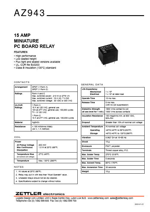
CONTACTSArrangement SPST (1 Form A)SPDT (1 Form C)RatingsForm A and CMax. switched power: 210 W or 2770 VA Max. switched current: 15 A AC, 7 A DCMax. switched voltage: 30 VDC or 300 VAC UL/CUR 1 Form ARatings15 A at 125 VAC, general use10A at 277 VAC, general use, 100,000 cycles TV - 5 120 VAC1 Form C10 A at 277 VAC, general use, 100,000 cyclesMaterial AgSnO 2Resistance< 100 milliohms initally (24 V, 1 A method)ZET TLERelectronicsTelephone +44 (0) 1582 599 600 Fax +44 (0) 1582 599 700Logistic Design (UK) Limited. Unit 3, Eagle Centre Way, Luton LU4 9US sales@ 2000-01-21GENERAL DATALife ExpectancyMechanical 1 x 10⁶Electrical 1 x 10⁵at rated load Operate Time 10 ms max.Release Time5 ms max.(with no coil suppression)Dielectric Strength 1500 Vrms contact to coil (at sea level for 1 min.)1000 Vrms across contacts Insulation Resistance 100 megohms min. at 500 VDC,50% RHDropoutGreater than 10% of nominal coil voltage Ambient TemperatureAt nominal coil voltage Operating -40°C(-40°F) to 95°C(203°F)Storage-40°C(-40°F) to 130°C(266°F)Vibration 0.062" DA at 10–55 Hz Shock10 gEnclosure P.B.T. polyesterTerminalsTinned copper alloy, P.C.Max. Solder Temp.270°C (518°F)Max. Solder Time 5 seconds Max. Solvent Temp.80°C (176°F)Max. Immersion Time 30 seconds Weight10 gCOILPowerAt Pickup Voltage 203 mWMax Continuous 1.0 W at 20°C (68°F)Dissipation Temperature Rise27°C (49°F)(at nominal coil voltage)TemperatureMax. 130°C (266°F)15 AMP MINIATUREPC BOARD RELAYFEATURES •High performance •Low seated height•Flux tight and sealed versions available •UL, CUR file E43203•Class B insulation (130°C) standardNOTES1.All values at 20°C (68°F).2.Relay may pull in with less than “Must Operate” value.3.Unsealed relays should not be dip cleaned.4.Specifications subject to change without notice.2000-01-21ZET TLERelectronicsTelephone +44 (0) 1582 599 600 Fax +44 (0) 1582 599 700Logistic Design (UK) Limited. Unit 3, Eagle Centre Way, Luton LU4 9US sales@ RELAY ORDERING DATASTANDARD RELAYSCOIL SPECIFICATIONSORDER NUMBERNominal CoilMax. ContinuousCoil ResistanceMust OperateUnsealed Sealed VDC VDC ±10%VDC 58.3703.8AZ943–1CH–5D AZ943–1CH–5DE 610.0100 4.5AZ943–1CH–6D AZ943–1CH–6DE 915.0225 6.8AZ943–1CH–9D AZ943–1CH–9DE 1220.04009.0AZ943–1CH–12D AZ943–1CH–12DE 1830.090013.5AZ943-1CH-18D AZ943-1CH-18DE 2440.01,60018.0AZ943–1CH–24D AZ943–1CH–24DE 4867.06,20036.0AZ943–1CH–48DAZ943–1CH–48DESubstitute “1AH” in place of “1CH” to indicate 1 Form A contact.Dimensions in inches with metric equivalents in parentheses. Tolerance: ± .010"。
ADN8810 12位高输出电流源数据手册(版本C)说明书
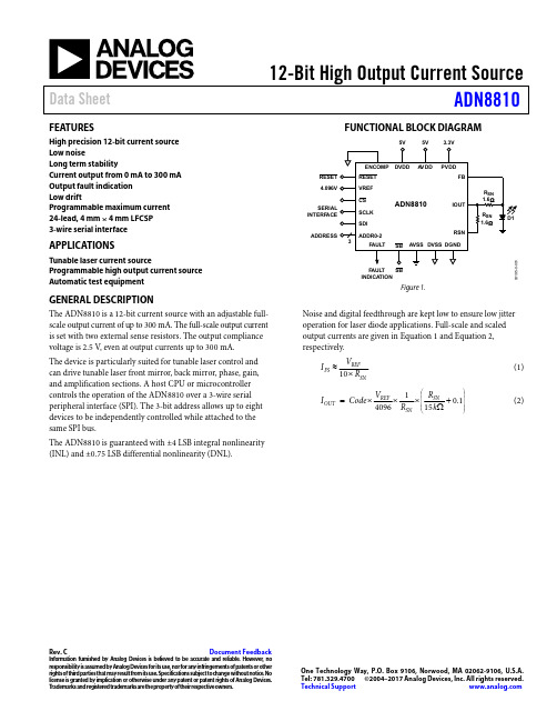
12-Bit High Output Current Source Data Sheet ADN8810Rev. C Document FeedbackInformation furnished by Analog Devices is believed to be accurate and reliable. However, noresponsibility is assumed by Analog Devices for its use, nor for any infringements of patents or other rights of third parties that may result from its use. Specifications subject to change without notice. No license is granted by implication or otherwise under any patent or patent rights of Analog Devices. T rademarks and registered trademarks are the property of their respective owners. O ne Technology Way, P.O. Box 9106, Norwood, MA 02062-9106, U.S.A. Tel: 781.329.4700 ©2004–2017 Analog Devices, Inc. All rights reserved. Technical Support FEATURESHigh precision 12-bit current sourceLow noiseLong term stabilityCurrent output from 0 mA to 300 mA Output fault indicationLow driftProgrammable maximum current24-lead, 4 mm × 4 mm LFCSP3-wire serial interface APPLICATIONSTunable laser current source Programmable high output current source Automatic test equipmentFUNCTIONAL BLOCK DIAGRAM3195-0 RESET4.096VSERIALINTERF ACEADDRESSSBF AULTINDICA TIONFigure 1.GENERAL DESCRIPTIONThe ADN8810 is a 12-bit current source with an adjustable full-scale output current of up to 300 mA. The full-scale output current is set with two external sense resistors. The output compliance voltage is 2.5 V, even at output currents up to 300 mA.The device is particularly suited for tunable laser control and can drive tunable laser front mirror, back mirror, phase, gain, and amplification sections. A host CPU or microcontroller controls the operation of the ADN8810 over a 3-wire serial peripheral interface (SPI). The 3-bit address allows up to eight devices to be independently controlled while attached to the same SPI bus.The ADN8810 is guaranteed with ±4 LSB integral nonlinearity (INL) and ±0.75 LSB differential nonlinearity (DNL). Noise and digital feedthrough are kept low to ensure low jitteroperation for laser diode applications. Full-scale and scaledoutput currents are given in Equation 1 and Equation 2,respectively.SNREFFS RVI⨯≈10(1)⎪⎪⎪⎪⎭⎫⎝⎛+Ω⨯⨯⨯=1.01514096kRRVCodeI SNSNREFOUT(2)ADN8810Data SheetRev. C | Page 2 of 14TABLE OF CONTENTSFeatures .............................................................................................. 1 Applications ....................................................................................... 1 Functional Block Diagram .............................................................. 1 General Description ......................................................................... 1 Revision History ............................................................................... 2 Specifications ..................................................................................... 3 Timing Characteristics ................................................................ 4 Absolute Maximum Ratings ............................................................ 5 ESD Caution .................................................................................. 5 Pin Configuration and Function Descriptions ............................. 6 Typical Performance Characteristics ............................................. 7 Terminology ...................................................................................... 9 Functional Description (10)Setting Full-Scale Output Current ........................................... 10 Power Supplies ............................................................................ 10 Serial Data Interface ................................................................... 10 Standby and Reset Modes ......................................................... 11 Power Dissipation....................................................................... 11 Using Multiple ADN8810 Devices for Additional Output Current ......................................................................................... 11 Adding Dither to the Output Current ..................................... 12 Driving Common-Anode Laser Diodes ................................. 12 PCB Layout Recommendations ............................................... 13 Suggested Pad Layout for CP-24 Package ............................... 13 Outline Dimensions ....................................................................... 14 Ordering Guide .. (14)REVISION HISTORY11/2017—Rev. B. to Rev. CChanged R S to R SN .......................................................... Throughout Change to Figure 1 ........................................................................... 1 Changes to Maximum Full-Scale Output Current Parameter and Power Supply Rejection Ratio Parameter, Table 1 ................ 3 Moved Timing Characteristics Section, Table 2, and Figure 2 ..... 4 Added Lead Temperature Range (Soldering 10 sec) Parameter, Table 3 ................................................................................................ 5 Changes to Figure 3 and Table 4 ..................................................... 6 Changes to Setting Full-Scale Output Current Section ............. 10 Changes to Adding Dither to the Output Current Section,Figure 20, and Figure 21 ................................................................ 12 Changes to PCB Layout Recommendations Section andFigure 25 .......................................................................................... 13 Updated to Outline Dimensions .................................................. 14 3/2016—Rev. A to Rev. BChanges to Figure 3 and Table 4 ...................................................... 7 Updated Outline Dimensions ....................................................... 15 Changes to Ordering Guide . (15)4/2009—Rev. 0 to Rev. A Changes to Table 3 ............................................................................. 6 Changes to Figure 25 ...................................................................... 14 Updated Outline Dimensions ....................................................... 15 Changes to Ordering Guide . (15)1/2004—Revision 0: Initial VersionData Sheet ADN8810 SPECIFICATIONSAVDD = DVDD = 5 V, PVDD = 3.3 V, AVSS = DVSS = DGND = 0 V, T A = 25°C, covering output current (I OUT) from 2% full-scale current (I FS) to 100% I FS, unless otherwise noted.Rev. C | Page 3 of 14ADN8810Data SheetRev. C | Page 4 of 141 With respect to AVSS. 2R SN = 20 Ω. 3See Table 2 for timing specifications.TIMING CHARACTERISTICS1, 21 Guaranteed by design. Not production tested.2Sample tested during initial release and after any redesign or process change that may affect these parameters. All input signals are measured with tr = tf = 5 ns (10% to 90% of DVDD) and timed from a voltage level of (V IL + V IH )/2.SCLKC SSDIRESET*ADDRESS BIT A3 MUST BE LOGIC LOW03195-0-002Figure 2. Timing DiagramData SheetADN8810Rev. C | Page 5 of 14ABSOLUTE MAXIMUM RATINGSTable 3.Parameter Rating Supply Voltage 6 VInput VoltageGND to V S + 0.3 V Output Short-Circuit Duration to GND IndefiniteStorage Temperature Range −65°C to +150°C Operating Temperature Range−40°C to +85°C Junction Temperature Range, CP Package −65°C to +150°C Lead Temperature Range (Soldering 10 sec)300°CStresses at or above those listed under Absolute Maximum Ratings may cause permanent damage to the product. This is a stress rating only; functional operation of the product at these or any other conditions above those indicated in the operational section of this specification is not implied. Operation beyond the maximum operating conditions for extended periods may affect product reliability.ESD CAUTIONADN8810Data SheetRev. C | Page 6 of 14PIN CONFIGURATION AND FUNCTION DESCRIPTIONS03195-0-003FAULT ADDR0ADDR1FB RSN ADDR2NICVREF AVDD AVSS NIC DVSS117P V D D I O U T I O U T P V D D 1E N C O M P S B NOTES1. NIC = NOT INTERNALLY CONNECTED.2. EXPOSED PAD. CONNECT THE EXPOSED PAD TO DGND.Figure 3. Pin ConfigurationData SheetADN8810Rev. C | Page 7 of 14TYPICAL PERFORMANCE CHARACTERISTICSCODE1.2–0.84,500500I N L E R R O R (L S B )1,0001,5002,0002,5003,0003,5004,0001.00.2–0.2–0.4–0.60.80.600.403195-0-005Figure 4. Typical INL PlotCODE0.4–0.304,500500D N LE R R O R (L S B )1,0001,5002,0002,5003,0003,5004,0000.1–0.1–0.20.300.203195-0-006Figure 5. Typical DNL PlotTEMPERATURE (°C)0.200.15–0.20–4085–15∆I N L (L S B )1035600–0.05–0.10–0.150.100.0503195-0-007Figure 6. ∆INL vs. TemperatureTEMPERATURE (°C)0.200.15–0.20–4085–15∆D N L (L S B )1035600–0.05–0.10–0.150.100.0503195-0-008Figure 7. ∆DNL vs. TemperatureTEMPERATURE (°C)0.2580.2570.250–4085–15F U L L -S C A L E O U T P U T (A )1035600.2540.2530.2520.2510.2560.255R SN = 1.6Ω03195-0-009Figure 8. Full-Scale Output vs. TemperatureTEMPERATURE (°C)20.76520.75520.720–4085–15F U L L -S C A L E O U T P U T (m A )10356020.74020.73520.73020.72520.75020.745R SN = 20Ω20.76003195-0-010Figure 9. Full-Scale Output vs. TemperatureADN8810Data SheetRev. C | Page 8 of 14TEMPERATURE (°C)0.500.35I P V D D (m A )0.200.150.100.050.300.250.400.4503195-0-011Figure 10. PVDD Supply Current (I PVDD ) vs. Temperature120I D V D D (µA )864210TEMPERATURE (°C)03195-0-012Figure 11. DVDD Supply Current (I DVDD ) vs. Temperature1.51.0I A V D D (m A )1.41.31.21.1TEMPERATURE (°C)03195-0-013Figure 12. AVDD Supply Current (I AVDD ) vs. TemperatureFREQUENCY (Hz)100k1O U T P U T I M P E D A N C E (Ω)1k1001010k03195-0-014Figure 13. Output Impedance vs. FrequencyTIME (1µs/DIV)CSI OUTV O L T A GE (2.7V /D I V )03195-0-015Figure 14. Full-Scale Settling TimeTIME (200ns/DIV)CSI OUT03195-0-016Figure 15. 1 LSB Settling TimeData SheetADN8810Rev. C | Page 9 of 14TERMINOLOGYRelative AccuracyRelative accuracy or integral nonlinearity (INL) is a measure of the maximum deviation, in least significant bits (LSBs), from an ideal line passing through the endpoints of the DAC transfer function. Figure 4 shows a typical INL vs. code plot. The ADN8810 INL is measured from 2% to 100% of the full-scale (FS) output.Differential NonlinearityDifferential nonlinearity (DNL) is the difference between the measured change and the ideal 1 LSB change between any two adjacent codes. A specified differential nonlinearity of ± 1 LSB maximum ensures monotonicity. The ADN8810 is guaranteed monotonic by design. Figure 5 shows a typical DNL vs. code plot . Offset ErrorOffset error, or zero-code error, is an interpolation of the output voltage at code 0x000 as predicted by the line formed from the output voltages at code 0x040 (2% FS) and code 0xFFF (100% FS). Ideally, the offset error is 0 V . Offset error occurs from a combination of the offset voltage of the amplifier and offset errors in the DAC. It is expressed in LSBs.Offset DriftThis is a measure of the change in offset error with a change in temperature. It is expressed in (ppm of full-scale range)/°C. Gain ErrorGain error is a measure of the span error of the DAC. It is the deviation in slope of the output transfer characteristic from ideal. The transfer characteristic is the line formed from the output voltages at code 0x040 (2% FS) and code 0xFFF (100% FS). It is expressed as a percent of the full-scale range.Compliance VoltageThe maximum output voltage from the ADN8810 is a function of output current and supply voltage. Compliance voltage defines the maximum output voltage at a given current and supply voltage to guarantee the device operates within its INL, DNL, and gain error specifications.Output Current Change vs. Output Voltage ChangeThis is a measure of the ADN8810 output impedance and is similar to a load regulation spec in voltage references. For a given code, the output current changes slightly as output voltage increases. It is measured as an absolute value in (ppm of full-scale range)/V .O U T P U T V O L T A G E03195-0-004Figure 16. Output Transfer FunctionADN8810Data SheetRev. C | Page 10 of 14FUNCTIONAL DESCRIPTIONThe ADN8810 is a single 12-bit current output digital-to-analog converter (DAC) with a 3-wire SPI interface. Up to eight devices can be independently programmed from the same SPI bus. The full-scale output current is set with two external resistors. The maximum output current can reach 300 mA. Figure 17 shows the functional block diagram of the ADN8810.03195-0-017Figure 17. Functional Blocks, Pins, and Internal ConnectionsSETTING FULL-SCALE OUTPUT CURRENTTwo external resistors set the full-scale output current from the ADN8810. These resistors are equal in value and are labeled R SN in Figure 1. Use 1% or better tolerance resistors to achieve the most accurate output current and the highest output impedance.Equation 3 shows the approximate full-scale output current. The exact output current is determined by the data register code as shown in Equation 4. The variable code is an integer from 0 to 4095, representing the full 12-bit range of the ADN8810.SNFS R I ×≈10096.4(3)+Ω××=1.0151000,1k R R Code I SN SN OUT(4)The ADN8810 is designed to operate with a 4.096 V referencevoltage connected to VREF. The output current is directly proportional to this reference voltage. To achieve the bestperformance, use a low noise precision (the ADR292, ADR392, or REF198 is recommended).POWER SUPPLIESThere are three principal supply current paths through the ADN8810: •AVDD provides power to the analog front end of the ADN8810 including the DAC. Use this supply line topower the external voltage reference. For best performance, AVDD must be low noise.•DVDD provides power for the digital circuitry. Thisincludes the serial interface logic, the SB and RESET logic inputs, and the FAULT output. Tie DVDD to the same supply line used for other digital circuitry. It is not necessary for DVDD to be low noise.•PVDD is the power pin for the output amplifier. It canoperate from as low as 3.0 V to minimize power dissipation in the ADN8810. For best performance, PVDD must be low noise.Current is returned through the following three pins: •AVSS is the return path for both AVDD and PVDD. This pin is connected to the substrate of the die as well as the slug on the bottom of the lead frame chip scale package (LFCSP). For single-supply operation, connect this pin to a low noise ground plane.•DVSS returns current from the digital circuitry powered by DVDD. Connect DVSS to the same ground line or plane used for other digital devices in the application.•DGND is the ground reference for the digital circuitry. In a single-supply application, connect DGND to DVSS.For single-supply operation, set AVDD to 5 V , set PVDD from 3.0 V to 5 V , and connect AVSS, AGND, and DGND to ground.SERIAL DATA INTERFACEThe ADN8810 uses a serial peripheral interface (SPI) with three input signals: SDI, CLK, and CS . Figure 2 shows the timing diagram for these signals.Data applied to the SDI pin is clocked into the input shift register on the rising edge of CLK. After all 16 bits of the data-word have been clocked into the input shift register, a logic high on CS loads the shift register byte into the ADN8810. If more than 16 bits of data are clocked into the shift register before CS goes high, bits are pushed out of the register in first-in first-out (FIFO) fashion.The four MSB of the data byte are checked against the address of the device. If they match, the next 12 bits of the data byte are loaded into the DAC to set the output current. The first bit (MSB) of the data byte must be a logic zero, and the following three bits must correspond to the logic levels on pins ADDR2, ADDR1, and ADDR0, respectively, for the DAC to be updated. Up to eight ADN8810 devices with unique addresses can be driven from the same serial data bus.Table 5 shows how the 16-bit DATA input word is divided into an address byte and a data byte. The first four bits in the input word correspond to the address. Note that the first bit loaded (A3) must always be zero. The remaining bits set the 12-bit data byte for the DAC output. Three example inputs are demonstrated.•Example 1: This SDI input sets the device with an address of 111 to its minimum output current, 0 A. Connecting the ADN8810 pins ADDR2, ADDR1, and ADDR0 to VDD sets this address.• Example 2: This input sets the device with an address of 000 to a current equal to half of the full-scale output. •Example 3: The ADN8810 with an address of 100 is set to full-scale output.STANDBY AND RESET MODESApplying a logic low to the SB pin deactivates the ADN8810 and puts the output into a high impedance state. The device continues to draw 1.3 mA of typical supply current in standby. When logic high is reasserted on the SB pin, the output current returns to its previous value within 6 µs.Applying logic low to RESET sets the ADN8810 data register to all zeros, bringing the output current to 0 A. When RESET is deasserted, the data register can be reloaded. Data cannot be loaded into the device while it is in standby or reset mode.POWER DISSIPATIONThe power dissipation of the ADN8810 is equal to the output current multiplied by the voltage drop from PVDD to the output.()SN OUT OUT OUT DISS R I V PVDD I P ×−−×=²(5)The power dissipated by the ADN8810 causes a temperature increase in the device. For this reason, PVDD must be as low as possible to minimize power dissipation.While in operation, the ADN8810 die temperature, also known as junction temperature, must remain below 150°C to prevent damage. The junction temperature is approximatelyDISS JA A J P T T ×θ+=(6)where:T A is the ambient temperature in °C,θJA is the thermal resistance of the package (32°C/W). •Example 4: A 300 mA full-scale output current is required to drive a laser diode within an 85°C environment. The laser diode has a 2 V drop and PVDD is 3.3 V .Using Equation 5, the power dissipation in the ADN8810 is found to be 267 mW . At T A = 85°C, this makes the junction temperature 93.5°C, which is well below the 150°C limit. Note that even with PVDD set to 5 V , the junction temperature increases to only 110°C.USING MULTIPLE ADN8810 DEVICES FOR ADDITIONAL OUTPUT CURRENTConnect multiple ADN8810 devices in parallel to increase the available output current. Each device can deliver up to 300 mA of current. To program all parallel devices simultaneously, set all device addresses to the same address byte and drive all CS , SDI, and CLK from the same serial data interface bus. The circuit in Figure 18 uses two ADN8810 devices and delivers 600 mA to the pump laser.SERIAL INTERFACE (FROM µC OR DSP)I 600mA03195-0-018Figure 18. Using Multiple Devices for Additional Output CurrentTable 5. Serial Data Input ExamplesAddress Byte Data Byte SDI Input A3 A2 A1 A0D11 D10 D9 D8 D7 D6 D5 D4D3 D2 D1 D0 Example 1 0 1 1 1 0 0 0 0 0 0 0 0 0 0 0 0 Example 2 0 0 0 0 1 0 0 0 0 0 0 0 0 0 0 0 Example 31 01111 11 11 1 1 1 1ADDING DITHER TO THE OUTPUT CURRENTSome tunable laser applications require the laser diode bias current to be modulated or dithered. This is accomplished by dithering the V REF voltage input to the ADN8810. Figure 19 demonstrates one method.DITHERR203195-0-019Figure 19. Adding Dither to the Reference VoltageSet the gain of the dither by adjusting the ratio of R2 to R1. Increase C to lower the cutoff frequency of the high-pass filter created by C and R1. The cutoff frequency of Figure 19 is approximately 98 Hz.The AD8605 is recommended as a low offset, rail-to-rail input amplifier for this circuit.DRIVING COMMON-ANODE LASER DIODESThe ADN8810 can power common-anode laser diodes. These are laser diodes whose anodes are fixed to the laser module case. The module case is typically tied to either VDD or ground. For common anode to ground applications, a −5 V supply must be provided.In Figure 20, R SN sets up the diode current by the following equation:40965.16111.1096.4Code k R I SN ×Ω+×=(7)where Code is an integer value from 0 to 4095.Using the values in Figure 20, the diode current is 300.7 mA at a code value of 2045 (0x7FF), or half full-scale. This effectively provides 11-bit current control from 0 mA to 300 mA of diode current.The maximum output current of this configuration is limited by the compliance voltage at the IOUT pin of the ADN8810. The voltage at IOUT cannot exceed 1 V below PVDD, in this case, 4 V. The IOUT voltage is equal to the voltage drop across R S N plus the gate-to-source voltage of the external FET. For this reason, select a FET with a low threshold voltage.In addition, the voltage across the R SN resistor cannot exceed the voltage at the cathode of the laser diode. Given a forward laser diode voltage drop of 2 V in Figure 20, the voltage at the RSN pin (I × R SN ) cannot exceed 3 V . This sets an upper limit to the value of code in Equation 5.Although the configuration for anode-to-ground diodes is similar, the supply voltages must be shifted down to 0 V and −5 V , as shown in Figure 21. The AVDD, DVDD, and PVDD pins are connected to ground with AVSS connected to −5 V .The 4.096 V reference must also be referred to the −5 V supply voltage. The diode current is still determined by Equation 7. All logic levels must be shifted down to 0 V and −5 V levels as well. This includes RESET , CS , SCLK, SDI, SB , and all ADDR pins. Figure 22 shows a simple method to level shift a standard TTL or CMOS (0 V to 5 V) signal down using external FETs.NOTE: LEAVE FB WITH NO CONNECTION03195-0-020Figure 20. Driving Common-Anode-to-VDD Laser DiodesNOTE: LEAVE FB WITH NO CONNECTION03195-0-021Figure 21. Driving Common-Anode-to-Ground Laser Diodes with a NegativeSupplyRESETCS SCLK SDI03195-0-022Figure 22. Level Shifting TTL/CMOS LogicPCB LAYOUT RECOMMENDATIONSAlthough they can be driven from the same power supply voltage, keep DVDD and AVDD current paths separate on the printed circuit board (PCB) to maintain the highest accuracy; likewise for AVSS and DGND. Tie common potentials together at a single point located near the power regulator. This technique is known as star grounding and is shown in Figure 23. This method reduces digital crosstalk into the laser diode or load.LOGIC GROUNDRETURN03195-0-023Figure 23. Star Supply and Ground TechniqueTo improve thermal dissipation, solder the slug on the bottom of the LFCSP package be soldered to the PCB with multiple vias into a low noise ground plane. Connecting these vias to a copper area on the bottom side of the board further improves thermal dissipation.Use identical trace width and lengths for the two output sense resistors. These lengths are shown as X and Y in Figure 24. Differences in trace lengths cause differences in parasitic seriesresistance. Because the sense resistors can be as low as 1.37 Ω, small parasitic differences can lower both the output current accuracy and the output impedance. See the AN-619 Application Note for a sample layout for these traces.03195-0-024Figure 24. Use Identical Trace Lengths for Sense ResistorsSUGGESTED PAD LAYOUT FOR CP-24 PACKAGEFigure 25 shows the dimensions for the PCB pad layout for the ADN8810. The package is a 4 mm × 4 mm, 24-lead LFCSP . The metallic slug underneath the package must be soldered to a copper pad connected to AVSS, the lowest supply voltage to the ADN8810. For single-supply applications, this is ground. Use multiple vias to this pad to improve the thermal dissipation of the package.0.0270.011(0.28)0.020(0.50)CONTROLLING DIMENSIONS ARE IN MILLIMETERS03195-0-025Figure 25. Suggested PCB Layout for the CP-24-10 Pad LandingOUTLINE DIMENSIONS0.300.250.200.800.750.700.25 MIN2.202.10 SQ 2.000.50BSC0.500.400.30COMPLIANT TO JEDEC STANDARDS MO-220-WGGD-8.BOTTOM VIEWTOP VIEWSIDE VIEW4.104.00 SQ 3.900.05 MAX 0.02 NOM0.203 REFCOPLANARITY0.08PIN 1INDICATORFOR PROPER CONNECTION OF THE EXPOSED PAD, REFER TO THE PIN CONFIGURATION AND FUNCTION DESCRIPTIONSSECTION OF THIS DATA SHEET.02-21-2017-AEXPOSED PAD00SEATING PLANEDETAIL A (JEDEC 95)Figure 26. 24-Lead Lead Frame Chip Scale Package [LFCSP]4 mm × 4 mm Body and 0.75 mm Package Height(CP-24-10)Dimensions shown in millimetersORDERING GUIDEModel 1Temperature Range Package DescriptionPackage Option ADN8810ACPZ–40°C to +85°C 24-Lead Lead Frame Chip Scale Package [LFCSP] CP-24-10 ADN8810ACPZ-REEL7–40°C to +85°C 24-Lead Lead Frame Chip Scale Package [LFCSP] CP-24-101Z = RoHS Compliant Part.©2004–2017 Analog Devices, Inc. All rights reserved. Trademarks and registered trademarks are the property of their respective owners. D03195-0-11/17(C)。
上海拿华电子 ADWA埃达华系列酸度 氧化还原 说明书

上海拿华电子科技有限公司ADWA埃达华系列酸度/氧化还原(含税公开报价)分类型号配件技术参数公开报价AD1030AD2002B/1 可填充玻璃pH电极,BNC接头和1米电缆,AD5006不锈钢温度探头和1米电缆,pH4.01,pH7.01和pH10.01校正缓冲溶液(20ml/袋),电极冲洗溶液,电极支架,12 Vdc电源适配器和用户手册。
3点校正;范围:-2.00~16.00pH,分辨率:0.01/0.001,精度:±0.01/±0.002;范围:±2000mV,分辨率:0.1~±999.9mV/1,精度:±0.2mV~±699.9mV/±0.5mV~±999.9mV/±2mV4858.00AD1040AD2002B/1 可填充玻璃pH电极,BNC接头和1米电缆,AD5006不锈钢温度探头和1米电缆,pH4.01,pH7.01和pH10.01校正缓冲溶液(20ml/袋),电极冲洗溶液,电极支架,12 Vdc电源适配器和用户手册。
3点校正;范围:-2.00~16.00pH,分辨率:0.01/0.001,精度:±0.01/±0.002;范围:±2000mV,分辨率:0.1~±999.9mV/1,精度:±0.2mV~±699.9mV/±0.5mV~999.9mV/±2mV;带GLP功能5690.00AD1000AD2002B/1 可填充玻璃pH电极,BNC接头和1米电缆,AD5006不锈钢温度探头和1米电缆,pH4.01,pH7.01和pH10.01校正缓冲溶液(20ml/袋),电极冲洗溶液,电极支架,12 Vdc电源适配器和用户手册。
6点校正;范围:-2.00~16.00pH,分辨率:0.01/0.001,精度:±0.01/±0.002;范围:±2000mV,分辨率:0.1~±999.9mV/1,精度:±0.2mV~±699.9mV/±0.5mV~±999.9mV/±2mV;带RS232/USB&GLP功能8465.00AD1200(离子浓度计)AD2002B/1 可填充玻璃pH电极,BNC接头和1米电缆,AD5006不锈钢温度探头和1米电缆,pH4.01,pH7.01和pH10.01校正缓冲溶液(20ml/袋),电极冲洗溶液,电极支架,12 Vdc电源适配器和用户手册。
ADE-10H+中文资料

元器件交易网 Mini-Circuits - Specification for Frequency Mixer - ADE-10H
601.429 1.63 2.27 3.57 2.76 2.55 2.37 267.895 1.21 1.03 1.14 601.429 2.76 2.55 2.37 1.63 2.27 3.57 293.684 1.20 1.03 1.15 630.000 1.46 1.87 2.55 2.80 2.65 2.49 319.474 1.19 1.05 1.17 630.000 2.80 2.65 2.49 1.46 1.87 2.55 345.263 1.16 1.07 1.21 644.286 2.80 2.65 2.52 1.41 1.78 2.35 371.053 1.11 1.11 1.28 644.286 1.41 1.78 2.35 2.80 2.65 2.52 396.842 1.05 1.19 1.39 687.143 2.72 2.55 2.43 1.50 2.27 3.86 422.632 1.13 1.29 1.52 687.143 1.50 2.27 3.86 2.72 2.55 2.43 448.421 1.29 1.38 1.57 730.000 2.80 2.65 2.52 1.30 1.82 2.46 474.211 1.40 1.41 1.54 730.000 1.30 1.82 2.46 2.80 2.65 2.52 500.000 1.48 1.43 1.48
138.947 1.21 1.01 1.15
164.737 1.21 1.01 1.14
190.526 1.21 1.01 1.13
216.316 1.21 1.02 1.13
法国溯高美低压产品介绍

熔断器开关 Fuserbloc 32 – 1250 A
• Fuserbloc 32 – 1250 A
主要特点:
• 模块化设计,每极1个模块 • 63A 以下导轨固定 • IP2 (熔断器盖和端子盖) • 试验位子为标准配置 ( 400A以下 ) • 1 至 21 极 • 直接操作 • 正面柜外操作 • 侧面操作 (左侧和右侧) • 可设置辅助触点 • 熔断指示 • 背面连接
正常 / 应急控制 器
ATyS 6
ATyS 3
ATyS C20/C30/C40
SWITCHING RANGE GB 10/2005
ATyS 系列电流等级
ATyS 3:
ATyS 3s : 125 – 1800A,3P/4P 10个电流等级 ATyS 3e : 2000 – 3200A,3P/4P 3个电流等级
SWITCHING RANGE GB 10/2005
熔断器开关 Fuserbloc CD 25 – 32 A
Disconnectable Neutral
GB/DIN:
25A 和 32A (熔断器尺寸: 10x38 和 14x51) 3 极和 3极+ 开关或固定中心极
附件:
• 直接和柜外手柄 • 可断开中性极 • 熔断器熔断指示( DIN 尺寸14x51) • U 型辅助触点模块 • 模块化辅助触模块 • 2x2 可设置 U 型辅助触点
SWITCHING RANGE GB 10/2005
熔断器开关
FUSERBLOC 系列 25 – 1250 A
SWITCHING RANGE GB 10/2005
熔断器开关 Fuserbloc CD 25 – 32 A
ADG-12A02-D2系列(比例换向阀放大器)

+10VDC -10VDC
PWM
I
13
U
14
32位微处理器
PWM
I
15
U
MCU
16
比例阀
ZENY ®
Electro-hydraulic Control
QD18041 04.25
原理框图
ZENY ®
Electro-hydraulic Control
特性曲线图
3000
2400
1800
1200
QD18041 04.25
5
+10V
6
-10V
7
+24VDC
8
0 VDC
9
DA
10
DB
11
SG
12
N.C.
13
a+
14
a-
15
b+
16
b-
功能描述 模拟信号输入: 0…+-10V 或 4-20mA
备用 备用 参考电压 参考电压 外部电源输入
RS485 通讯接口
备用 比例电磁铁 A
比例电磁铁 B
乔存科技
4/8
ADG-12A-02-D2 系列
QD18041 04.25
数字式比例放大器
ADG-12A-02-D2 系列 40 系列
ZENY ®
Electro-hydraulic Control
目录
内容 特点 订货型号 技术数据 原理框图 输出特性曲线 引脚分配 接线范例 外形尺寸 软件设置画面
页码 1 2 2 3 4 4 5 6 7
特点
-适用于控制各种不带电气位移反馈的比例换向阀, 如力士乐型 4WRA6,4WRA10,ATOS,迪普玛等 。
Analog Devices IC (ADE) 产品系列简介说明书

Energy Measurement ProductsADE Product Family OverviewThe Analog Devices IC (ADE) family combines industry-leading data conversion technology with a fixed function digital signal processor (DSP) to perform the calculations essential to an electronic energy meter. The portfolio includes single-phase products and polyphase products for stepper motor and LCD display meter designs, with five critical measurements available: watt, V rms, I rms, VA, and VAR.With 175 million units deployed in the field, ADI has added to the portfolio the ADE71xx and ADE75xx product families that simplify energy meter design by providing all the features needed for an accurate, reliable, and fully functional energymeter with LCD display in a single IC.ADE Product Family • High accuracy exceeds IEC and ANSI standards • Proprietary 16-bit ADCs and DSP provide high accuracy over large variations in current, environmental conditions, and time • Reliability proven with over 175 million units deployed in the field• On-chip reference with low temperature drift (20 ppm to 30 ppm typ)• On-chip power supply monitoring• On-chip creep protection (no-load threshold)• Single 5 V supply • Low power consumption • Instantaneous active power output for calibration or interface to an MCU • Miswiring or reverse power indication• Tamper detection optionsADE Pulsed Output Products or Stepper Motor Display Meters • Exceeds IEC 61036/62053-21, IEC 60687/62053-22, ANSI C12.16, and ANSI C12.20• Active energy measurement with less than 0.1% error over a dynamic range of 500 to 1 at 25°C• Power consumption as low as 15 mW (typ) for single-phase products and 30 mW (typ) for polyphase products• Built-in current channelamplifier allows the use of low resistance, low cost shunts • Active energy, low frequency outputs directly driveelectromechanical counters • Single 5 V supplyADE Serial Interface Products for LCD Meters• Exceeds IEC 61036/62053-21, IEC 60687/62053-23 (for multifunction products), ANSI C12.16, and ANSI C12.20• Active energy measurement with less than 0.1% error over a dynamic range of 1000 to 1 at 25°C• Active energy and sampled waveform data• Multifunction products provide VAR, VA, V rms, and I rms • User-programmable power quality monitoring features • Digital calibration for power, phase, and offset• Serial peripheral interface (SPI) with interrupt request pin (IRQ)• Single 5 V supplyIntegrated Products for LCD Meters• Exceeds IEC 61036/62053-21, IEC 60687/62053-23 (for multifunction products), ANSI C12.16, and ANSI C12.20• Single chip solution integrates ADE measurement core for watts, VAR, VA, V rms, and I rms• 8052 MCU core with flash memory• 104-segment LCD driver with contrast control for low/high temperature visibility • Low power RTC (1.5 μA typ) with digital compensation for temperature performance • Power fail and batterymanagement with no external components• Reference with low temperature drift (5 ppm/°C typ)• Noninvasive in-circuitemulation/energymeterValue of ADE Products1. Proven TechnologyAnalog Devices is the market leader in sales of energy metering ICs with over 175 million meters deployed worldwide with ADE products.• Quality: Strict quality and test standards applied to ADE products throughout design and manufacturing stages ensure low meter production failure rate and uniform part-to-part characteristics.• Reliability: Accelerated life expectancy tests on ADE products, representing more than 60 years of field usage, reduce probability of meter failure due to IC failure.• Performance: Proprietary Σ-∆ ADCs provide excellent performance with an error of less than 0.1% over an extended current dynamic range.2. Ease of DesignAnalog Devices ADE solutions aim to simplify energy meter design, reduce system cost, and reduce time to market with:• Integration of ADCs and fixed function DSP on a single chip leading to a single IC energy meter• Integration of ADCs and fixed function DSP on a single chip reduces processing requirements, enabling the use of a lower cost MCU • Embedded essential energy calculations to ensure harmonic content is included (up to 233rd harmonics for watt-hour measurement)• Direct and flexible sensor interface without external gain amplifiers• Unparalleled design support including detailed data sheets, reference designs, application notes, evaluation tools, and technical support • Integrated MCU core, and all necessary peripherals, with field proven metering front end • Greater system control with minimized current consumption in battery mode3. Innovation and ChoiceAnalog Devices is committed to continuing its investment in the ADE product family and to enabling very competitive system costs while maintaining a high level of innovation.• 16 patents granted or pending on innovative energy measurement technology• Many energy measurement products currently available for single-phase and polyphase energy meters with more to come4. Quality• Samples from production lots constantly drawn for rigorous qualifications• ADI’s product analysis group continually addresses customer concerns and feedback on the quality of our products • Constant monitoring of electrical ppm failure rate of finished products• Electrical ppm failure rate is largely comprised of marginal parametric rejects that are fully functional but are most likely to experience failure in the field•ADI products have a consistently low ppm failure rate that reflects the stability and high quality of the manufacturing process• TIME DEPENDENT DIELECTRIC BREAKDOWN • ELECTROMIGRATION• HOT CARRIER INJECTION• THERMAL SHOCK SEQUENCE• TEMPERATURE CYCLING SEQUENCE• ELECTRICAL ENDURANCE—HTOL AND LTOL • EARLY LIFE FAILURE CHARACTERIZATION • HIGH TEMPERATURE STORAGE • MOISTURE ENDURANCE TEST • DIE SHEAR TEST• FABRICATION AND ASSEMBLY QUALIFICATION • ELECTRICAL STATIC DISCHARGE (ESD)• LATCH UPPRODUCTION QUALITY CONTROL SUPPLEMENTAL QUALIFICATIONS APPLICATION SPECIFIC QUALIFICATIONEND PRODUCT QUALIFICATIONFABRICATION QUALIFICATIONASSEMBLY QUALIFICATIONANALOG DEVICESSTANDARD QUALIFICATIONS LIST OF QUALIFICATIONSPASSEDPASSEDCUSTOMER FEEDBACK• BOND STRENGTH • BURN-IN SEQUENCE• CONSTANT ACCELERATION • HERMETICITY• HIGH TEMPERATURE STORAGE • INTERNAL WATER VAPOR TEST • LEAD FATIGUE • LID TORQUE• MARKING PERMANENCY • MECHANICAL SHOCK• MOISTURE SENSITIVITY CHARACTERIZATION• MOISTURE ENDURANCE SEQUENCE AND AUTOCLAVE • RESISTANCE TO SOLDERING HEAT • SOLDERABILITY• THERMAL IMPEDANCE• VIBRATION, VARIABLE FREQUENCY • X-RAY INSPECTIONReliabilityAnalog Devices conducted a high temperature operating lifetest (HTOL) to simulate aging of ADE products in the field.Method—ICs subjected to 150°C for 3000 hours:• With acceleration factor of 179×, the life expectancy correlates to 60 years at operating temperature of 60°C.• Four main parameters monitored: reference voltage, gain error, current, and voltage channel offset.Results—parameter distribution over time shows:• Negligible parameter distribution shifts.• Parameters maintain data sheet specifications.• Zero failures.Conclusions from HTOL test:• If other components in electronic meter have the same life expectancy, meter replacement is only needed every 60 years.• Proven stability and accuracy of digital energy measurement.Meter manufacturers must carefully select components to ensure that the overall reliability of electronic energy meter is maximized.10,000125OPERATING TEMPERATURE (°C)A C C E L E R A T I O N F A C T O R10001001010,0001L I F E T I M E (Y e a r s )100010010303540455055606570758085PerformanceThe unsurpassed accuracy of power calculation over a very wide dynamic range, harmonics, and stability over time are the primary reasons why ADE ICs are preferred by many meter manufacturers around the world. The plot to the right highlights the typical performance of ADE ICs over a dynamic range of 1000:1 and temperature range of –40°C to +85°C. Even at a low power factor (PF = 0.5), the ICs maintain their high accuracy.0.4–0.4AMPSE R R O R (%)0.30.20.10–0.1–0.2–0.3Reliability Lifetime PredictionsTypical Performance for ADE ICs"%$"%$"%$&/&3(:.&"463&.&/5%41*/5&3/"- 7 QQN $4*/(-&$:$-& .$66"3541* *$8%53".108&3 4611-:$0/530-108&3 4611-:.0/*503*/(-%0103"%$*/5&3/"-3&4&5"%$5&.1&3"563&4&/403*/5&3/"- 147 ."9$)"3(& 16.1%"$-$% %3*7&3 4&(.&/541--*/5&3/"-$-0$,35$'-"4).&.03:"%& YY "%& YYSelection GuideADE71xx/ADE75xx: Energy Measurement Computing EngineThe ADE71xx/ADE75xx family builds on Analog Devices’ 10 years of experience in energy measurement to provide the best analog-to-digital converters combined with the advanced digital signal processing required to build an accurate, robust, and fully featured energy meter with LCD display.Energy Measurement Key Features:• Exceeds IEC 61036/62053-21,IEC 60687/62053-22, IEC 61268/62053-23, ANSI C12.16, and ANSI C12.20• 4-quadrant power and energy measurement for:• Active, reactive, and apparent• Tampering protection• 2 current inputs for line and neutral • Tampering algorithms integrated • Special energy accumulation modes• Shunt, current transformer, and di/dt current sensor connectivity enabled• 2 high precision pulse outputs for calibration • Power line quality: SAG, period/frequency, peak, zero-crossing• Large phase calibration (5° @ 50 Hz)• Wide measurement frequency bandwidth (14 kHz) for harmonic measurementADE71xx/ADE75xx: LCD DriverThe ADE71xx/ADE75xx family has a unique LCD driver capable of maintainingmaximum contrast on the LCD independently of the power supply level using charge-pump circuitry. This technology combined with the on-chip temperature measurement enables the lowest power operation and maximum readability of the energy meter LCD display.LCD Driver Key Features:• 104-segment LCD driver• Adjustable LCD voltage (5 V max) independent of the power supply (2.7 V min)• LCD freeze and hardware blink functions for low power operation in battery mode • Low offset to minimize LCD fluid biasingRTC Key Features:•1.5 μA current consumption•Low voltage operation: 2.4 V•2 ppm/LSB digital frequency adjustment for calibration and temperature compensation •Alarm and midnight interruptsADE71xx/ADE75xx: Real-Time ClockThe ADE71xx/ADE75xx family provides a low power RTC with nominal and temperature dependent crystal frequency compensation capabilities enabling low drift and high accuracy timekeeping. The RTC functionality is also maintained at low power supply (2.4 V) and over all power supply connections, extending the operating life of the energy meter in battery mode.ADE71xx/ADE75xx: Battery ManagementThe ADE71xx/ADE75xx family has unique battery management features enabling low power consumption in battery mode and optimal power supply management when line voltage is lost.Battery Management Key Features:•No external circuitry for battery switching•Power supply switching based on absolute level•Early warning of power supply collapse with SAG and preregulated power supply monitoring•Internal power supply always valid by hardware controlled switchover to batteryKey Features Maintained in Battery Mode:•Real-time clock for timekeeping•LCD display•Temperature measurement•Meter wake-up events such as RTC alarms, I/O, UART activitiesADE Development ToolsThe ADE71xx and ADE75xx family of products share a common set of tools designedto minimize design time while improving the part understanding. These tools arecomprised of:• Energy meter reference design• 1-pin emulator with isolated USB interface• Isolated USB to UART debugger interface• Downloader software• Evaluation software• Integrated development environment from well-known vendor• Firmware libraries for common and part specific functionsThe energy meter reference design integrates the main functions of an LCD meter withIR port and RS-485 communication, battery backup, two current sensors, antitamperinterface, and EEPROM interface while using the features of the ADE71xx and ADE75xxseries such as battery management, antitamper detection, temperature compensatedreal-time clock, and LCD driver contrast.The reference design is accompanied by code libraries and an example of systemintegration code allowing easy evaluation and further development of solution.Isolated USB communication boards for debugging and emulation provide a safesolution for code development when the meter is connected to the line.The ADE71xx and ADE75xx series can be used with integrated developmentenvironments (IDE) from open market vendors to simulate, compile, debug, anddownload assembly or C code. A free of charge IDE with unlimited assembly codecapability and 4 kB limited C code capability is included in the evaluation kit. Inaddition, the part can be evaluated with a UART interface and a PC by using theversatile evaluation tools and downloader.Single-Phase Energy Metering ICs with Integrated OscillatorThe AD71056, ADE7768, and ADE7769 are single-phase ICs that provide watt-hour information using pulse outputs that directly drive a stepper motor counter.The AD71056, ADE7768, and ADE7769 are pin-reduced versions of the ADE7755, with the enhancement of an on-chip, precisionoscillator circuit that serves as the clock source for the IC. The direct interface to low resistance, low cost shunt resistors also helps to lower the cost of a meter built with AD71056, ADE7768, or ADE7769.These products are pin compatible. The AD71056 and ADE7769 accumulate bidirectional power information, and the ADE7768accumulates power only in the positive direction providing flexibility for various billing schemes. The ADE7769 indicates when the power is below the no-load threshold by holding the calibration frequencypin high. This is useful to indicate a tampering or miswired condition.Single-Phase Energy Metering ICs with Antitamper FeaturesThe ADE7761B detects two common tampering conditions: “fault” condition (when loads are grounded to earth instead of connected to neutral wire or when the meter is bypassed with external wires) and “missing neutral” condition (when the voltage input and return current are missing). The ADE7761B incorporates a novel tampering detection scheme which indicates the fault or missing neutral conditions and allows the meter to continue accurate billing by continuous monitoring of the phase and neutral (return) currents. A fault is indicated when these currents differ by more than 6.25%, and billing continues using the larger of the two currents. The missing neutral condition is detected when no voltage input is present, and billing is continued based on the active current signal. The ADE7761B also includes a power-supply monitoring circuit which ensures that the voltage and current channels are matched,eliminating creep effects in the meter.Polyphase Energy Metering ICs with Pulse OutputThe ADE7752A, ADE7752B, and ADE7762 are polyphase ICs that provide watt-hour information using pulse outputs that can directly drive a stepper motor counter. Compatible with a wide range of 3-phase grid configurations, including 3-wire and 4-wire delta and wye distributions, each of these products can be used for 3-phase commercial and industrial revenue meters or submeters, 3-phase motors or generators, industrial control, and utility automation. The ADE7762 and ADE7752B are optimized for 3-phase, 3-wire applica-tions with no-load threshold and REVP indication based on the sum of the phases.To ensure that energy is billed properly under miswiring or tamper-ing conditions, any of the ICs can be set to accumulate based on the sum of the absolute value in each phase. The active power accumu-lation is signed by default.The ADE7762 has four additional logic output pins. These four pins drive six LEDs for prioritized indication of phase dropout and phasesequence error as well as reverse polarity per phase.ADE7752A and ADE7752B are pin compatible with the legacy ADE7752 and have up to a 50% power consumption reduction from ADE7752. The four additional pins of ADE7762 are located at the top of the package so that the same PCB may be used with an ADE7752A-, ADE7752B-, or ADE7762-based meter.10Single-Phase Energy Metering ICs with Serial InterfaceADI has a range of product offerings for single-phase energy measurement solutions requiring serial interface. The ADE7756 measures active energy and allows digital calibration of phase, offset, and gain through a serial port interface. The ADE7759 has a built-in digital integrator for direct interface with a di/dt sensor such as a Rogowski coil and includes the capability to interface with low resistance shunts and traditional current transformers. The ADE7753 provides active, apparent, and reactive energy measurements, and incorporates a built-in digital integrator to allow direct interface with a Rogowski coil sensor in addition to a low resistance shunt or CT. The ADE7763 provides the same functionality as the ADE7753 but without reactive energy measurement. All four of these ADE single-phase energy metering ICs with SPI are pin compatible for ease of design migration.11Polyphase Energy Metering ICs with Serial InterfaceADI has a selection of product offerings for3-phase energy measurement solutions requiring serial interface. The ADE7758 features second-order sigma-delta ADCs, and is designed formidrange 3-phase energy meters. For each phase, the chip measures active, reactive, and apparent energy, as well as rms voltage and rms current. These measurements are accessed via an SPI that allows a fully automated digital calibration. The ADE7758 interfaces with a variety of sensors, including current transformers and di/dt current sensors, such as Rogowski coils. Additionally, the ADE7758 provides a programmable frequency pulse output for both active and apparent orreactive power.Analog Devices, Inc.Worldwide Headquarters Analog Devices, Inc. One Technology Way P .O. Box 9106Norwood, MA 02062-9106 U.S.A.Tel: 781.329.4700 (800.262.5643, U.S.A. only)Fax: 781.461.3113Analog Devices, Inc. Europe Headquarters Analog Devices, Inc.Wilhelm-Wagenfeld-Str. 6 80807 Munich GermanyTel: 49.89.76903.0 Fax: 49.89.76903.157Analog Devices, Inc. Japan Headquarters Analog Devices, KK New Pier Takeshiba South Tower Building 1-16-1 Kaigan, Minato-ku, Tokyo, 105-6891 JapanTel: 813.5402.8200 Fax: 813.5402.1064Analog Devices, Inc. Southeast Asia Headquarters Analog Devices22/F One Corporate Avenue 222 Hu Bin Road Shanghai, 200021 ChinaTel: 86.21.5150.3000 Fax: 86.21.5150.3222©2007 Analog Devices, Inc. All rights reserved. Trademarks and registered trademarks are the property of their respective owners.Printed in the U.S.A. BR04915-5-8/07(A)/energymeter。
LTC1298 微功耗双通道采样12位A D转换器演示手册说明书

1DESCRIPTIOUThe LTC ®1298 is a micropower, 11.1ksps, two-channel sampling 12-bit A/D converter that draws only 1.25mW from a single 5V supply. The LTC1298 demo board pro-vides the user with a stable and consistent platform on which to evaluate the LTC1298 A/D converter. In addition,the LTC1298 demo board illustrates the layout and by-passing techniques required to obtain optimum perfor-mance from this part. The LTC1298 demo board is de-signed to be easy to use and requires only a 7V to 15V supply, a clock signal, and an analog input signal. As shown in the Board Photo, the LTC1298 is a very space efficient solution for A/D users. By combining a mi-cropower 12-bit A/D, sample-and-hold, two-channel mul-tiplexer, serial port, and auto shutdown circuit into a single 8-pin SOIC package, all the data acquisition circuitry including the bypass caps occupy an area of only 0.1square inch.This manual shows how to use the demo board. It includes timing diagrams, power supply requirements, and analog input range information. Additionally, a schematic, parts list, drawings, and dimensions of all the PC board layers are included. Finally, an explanation of the layout andbypass strategies used in this board allows anyone de-signing a PC board to achieve maximum performance from the device.12-Bit A/D ConverterDemo Boards Proven µPower 12-Bit ADC Surface Mount Layout s On-Chip Two-Channel MulitplexersActual ADC Footprint Only 0.1 Inch 2 Including Bypass Capacitorss 71dB SINAD, 84dB THD and ±0.25LSB DNL sGerber Files for This Circuit Board Are Available.Call the LTC Factory.FEATURESTYPICAL PERFOR A CE CHARACTERISTICS A D BOARD PHOTOU UW DC045 • BP01SAMPLE FREQUENCY (Hz)0.1k11010010001k 10k 100kLT1286/98 G03S U P P L Y C U R RE N T (µA )Supply Current vs Sample Rate2DEMO MANUAL DC045W W T O P V I E WA EC 1DEMO MANUAL DC045 REFERENCEDESIGNATOR QUANTITY PART NUMBER DESCRIPTION VENDOR TELEPHONE C11TAJD476M01047µF 10V 20%, Tantalum Capacitor AVX(207) 282-5111 C2 to C5, C85GRM42-6X7R104K050AD0.1µF 50V 10%, X7R Chip Capacitor Murata Erie(814) 237-1431 C6, C9, C12312063G105ZATMA1µF 25V +80%/–20%, Y5V Chip Capacitor AVX(803) 448-9411 C71TAJB106M01010µF 10V 20%, Tantalum Capacitor AVX(207) 282-5111 C10112062R150K9BB215pF 50V 10% NPO Chip Capacitor Philips(407) 744-4200 C11108055A470GATBA47pF 50V 2% NPO Chip Capacitor AVX(803) 448-9411 D0 to D1112SF1-BR Red LED Data Display(800) 421-6815 E1, E22575-4Banana Jack Keystone(718) 956-8900 E3 to E531502-2Turret Keystone(718) 956-8900 JP11TSW-101-07-G-D Header Samtec(800) 726-8329 JP21TSW-104-07-G-D Header Samtec(800) 726-8329 JP31TSW-107-06-G-D Header Samtec(800) 726-8329 JP41TSW-105-07-G-SN Header Samtec(800) 726-8329 J11227699-3BNC Connector AMP(717) 564-0100 R1 to R1212CR32-621J-T620Ω 1/8W 5% 1206 Chip Resistor AVX(803) 448-9411 R13 to R153CT32-223J-T22k 1/8W 5% 1206 Chip Resistor AVX(803) 448-9411 R161CT32-102J-T1k 1/8W 5% 1206 Chip Resistor AVX(803) 448-9411 R171CT32-103J-T10k 1/8W 5% 1206 Chip Resistor AVX(803) 448-9411 R181CT32-5101J-T51Ω 1/8W 5% 1206 Chip Resistor AVX(803) 448-9411 S1190HBW03S DIP Switch Grayhill(708) 354-1040 U1174HC592IC Toshiba(408) 737-9844 U2174HC165IC Toshiba(408) 737-9844 U31LTC1298CS8IC LTC(408) 432-1900 U41LTC1021DCS8-5IC LTC(408) 432-1900 U5174HC14IC Texas Instruments(800) 336-5236 U61LT1121CST-5IC LTC(408) 432-1900 U7, U8274HC595IC Toshiba(408) 737-9844 4HTSP-3Plastic Stand.Micro Plastic(501) 453-88615SNT-100-BK-5Shunt Samtec(800) 726-832944/40 × 3/8Steel ScrewPARTS LISTOPERATIOUOPERATING THE BOARDPowering the BoardTo use the demo board, apply a 7V to 15V power source capable of supplying ≥100mA to the banana jacks (E1 and E2). Be careful to observe the correct polarity. On-board regulators provide 5V to the LTC1298’s V CC pin. LT1121-5 and LT1021 regulators generate 5V for the digital circuitry and ADC, respectively.Applying the Analog InputAnalog input signals are applied to the LTC1298’s two-channel (CH0 and CH1) input multiplexer through the demonstration board’s turret terminals E3 (CH0) and E4 (CH1). The input signals’ ground reference is applied to turret terminal E5. The analog signal input range is 0V to 5V. Optimum performance is achieved using a signal source that has low output impedance, is low noise, and34DEMO MANUAL DC045OPERATIOUhas low distortion. Signal generators such as the B & K Type 1051 sine generator give excellent results.Applying the Clock SignalThe clock signal is applied to BNC connector J1 and the CS signal is generated on the board. The clock input uses TTL or CMOS levels. The maximum clock frequency is 200kHz. While the clock signal is active, a high-to-low logic level transition is generated on the LTC1298’s CS input which initiates a conversion. The data transfer is shown in the timing diagrams (Figure 1).Reading the Output DataThe LTC1298 serial data outputs are buffered by the two 74HC595 latches and are available as a parallel output on connector JP3. The latches are used to drive the LEDs D0to D11. (Refer to the LTC1298 data sheet for details on different digital interface modes.)The LTC1298 output data is in unipolar format. A Data Ready line, RDY, (JP3 pin 13) is provided to latch the data.Data is valid on the rising edge of RDY. Connector JP3 has one ground pin (JP3 pin 14). Connect this pin to the data receiving system’s digital ground.MSB-First Data (MSBF = 0)Figure 1. Timing DiagramD CLKODD/ CSD LTC1286/98 • F02*AFTER COMPLETING THE DATA TRANSFER, IF FURTHER CLOCKS ARE APPLIED WITH CS LOW, THE ADC WILL OUTPUT ZEROS INDEFINITELY.ODD/ D t DATA : DURING THIS TIME, THE BIAS CIRCUIT AND THE COMPARATOR POWER DOWN AND THE REFERENCE INPUTBECOMES A HIGH IMPEDANCE NODE. WITH CS LOW AND THE CLOCK ACTIVE, THE OUTPUT ON D OUT IS EITHER LSB-FIRST DATA (MSBF = 0) OR ZEROS (MSBF = 1).MSB-First Data (MSBF = 1)5DEMO MANUAL DC045OPERATIOUTable 1.JUMPER JUMPER NAME JUMPER CONNECTIONJP1LED EnableShorted to enable LEDs. Open to disable the LEDs.JP2A CS Shorted for normal operation. If open, the CS line can be driven externally to select or deselect the LTC1286.JP2B CLK Shorted for normal operation. If open, the CLK line can be driven externally to clock the LTC1286.JP2C D OUT Shorted for normal operation. If open, the D OUT line can drive a scope probe.JP2DD INShorted for normal operation. If open, the D IN line can be driven externally to configure the input multiplexer.The LTC1298’s data word can be acquired with a logic analyzer. By using a logic analyzer that has a PC-compat-ible floppy drive, (such as an HP1663A), conversion data can be stored on a disk and easily transferred to a PC. Once the data is transfered to a PC, programs such as Mathcad or Excel can be used to calculate FFTs. The FFTs can be used to obtain LTC1298 AC specifications such as signal-to-noise ratio and total harmonic distortion.LEDs D0 to D11 provide a visual display of the LTC1298’s digital output word. D0 is the LSB and D11 is the MSB.Jumper JP1 can be removed to disable the LEDs, reducing supply consumption by up to 56mA.Driving CS, D IN , and CLKJumpers for CS, CLK, D IN , and D OUT (JP2) are shorted for normal operation. The jumpers can be removed and CS,D IN , and CLK lines can be externally driven if desired. See the LTC1298 data sheet for details on driving these YOUTThe use of separate analog and digital ground planes is a good practice for a well designed LTC1298 PC board. Theproper way to make the analog and digital ground planes can be seen by examining the solder side of the PCB layout. The two ground planes are completely isolated except for one connection at the power supply ground input, E1. The two ground planes follow the same path on the component and solder sides of the board to reduce coupling between the ground planes. Also ensure that the analog ground plane’s solder side has a limited number of plane-breaking traces within it. Any trace that opens a portion of the ground plane may reduce the ground plane’s efficiency. Further, the analog and digital traces do not cross each other (whether on the board’s top or bottom side) or run adjacent to each other.BYPASSINGIt is important to place the supply/reference bypass ca-pacitor as close as possible to the LTC1298’s supply/reference pin. The ground side of the capacitor should have a very short path to analog ground. The V CC /V REF pins should be bypassed with high quality ceramic capaci-tors of at least 0.1µF.6DEMO MANUAL DC045OPERATIOUTable 2.INPUT/OUTPUT PINFUNCTIONJ1Clock InputE1GroundE27V to 15V at ≥100mA CH0Multiplexer Input Channel 0CH1Mulitplexer Input Channel 1AGND Input signals’ ground reference JP3-1D0 (LSB)JP3-2D1JP3-3D2JP3-4D3JP3-5D4JP3-6D5INPUT/OUTPUT PINFUNCTIONJP3-7D6JP3-8D7JP3-9D8JP3-10D9JP3-11D10JP3-12D11 (MSB)JP3-13RDY. Can be used by an external system to latch the ADC’s output. Latch data on the rising edge.JP3-14Ground. Connect to the digital ground of a data receiving system.PCB LAYOUT A D FILU WComponent Side Silkscreen7DEMO MANUAL DC045Information furnished by Linear Technology Corporation is believed to be accurate and reliable.However, no responsibility is assumed for its use. Linear Technology Corporation makes no represen-tation that the interconnection of its circuits as described herein will not infringe on existing patent rights.PCB LAYOUT A D FILUWCircuit: Component SideCircuit: Solder SideComponent Side Solder MaskSolder Side Solder Mask8DEMO MANUAL DC045SYMBOL DIAMETER # OF HOLESA 0.1254B 0.2102C 0.0943D 0.035129E 0.04029F 0.0455UNMARKED0.01897TOTAL HOLES269Linear Technology Corporation1630 McCarthy Blvd., Milpitas, CA 95035-7487(408) 432-1900 qFAX : (408) 434-0507 qTELEX : 499-3977© PC FAB DRAWI GUA DAFEX8EX5F FF FAE X 14D X 128B C CC BEE NOTES:1.MATERIAL IS FR4, 0.062˝ THICK WITH 2 OUNCE COPPER.2.PCB WILL BE DOUBLE-SIDED WITH PLATED THROUGH-HOLES.3.HOLE SIZES ARE AFTER PLATING. PLATED THROUGH-HOLE WALL THICKNESS MINIMUM 0.0014˝ (1OZ.).E PADMASTER PROCESS.5.SOLDER MASK BOTH SIDES WITH PC401 USING FILM PROVIDED.6.SILKSCREEN COMPONENT SIDE USING FILM E WHITE, NON-CONDUCTIVE INK.7.ALL DIMENSIONS ARE IN INCHES.。
- 1、下载文档前请自行甄别文档内容的完整性,平台不提供额外的编辑、内容补充、找答案等附加服务。
- 2、"仅部分预览"的文档,不可在线预览部分如存在完整性等问题,可反馈申请退款(可完整预览的文档不适用该条件!)。
- 3、如文档侵犯您的权益,请联系客服反馈,我们会尽快为您处理(人工客服工作时间:9:00-18:30)。
元器件交易网 Mini-Circuits - Specification for Frequency Mixer - ADE-12H
817.948 6.05 3.06 2.61 3.38 2.92 2.76 136.316 3.79 1.30 1.13 830.000 5.03 2.96 2.65 3.16 2.84 2.68 148.947 3.50 1.28 1.13 880.000 8.31 3.64 3.26 3.50 2.96 2.76 161.579 3.64 1.29 1.14 930.000 4.64 2.92 2.92 3.16 2.88 2.68 174.210 3.38 1.27 1.14 980.000 7.28 3.32 3.01 3.21 2.61 2.49 186.842 3.50 1.28 1.15 1030.000 4.32 2.92 3.06 2.80 2.43 2.23 199.474 3.38 1.27 1.15 1080.000 5.33 3.16 3.06 2.80 2.49 2.30 212.105 3.50 1.29 1.16 1130.000 4.32 2.88 3.01 2.88 2.55 2.40 224.737 3.21 1.27 1.16 1180.000 4.22 3.16 3.38 2.88 2.61 2.46 237.368 3.44 1.28 1.17 1230.000 4.32 2.96 3.38 3.16 2.76 2.55 250.000 3.21 1.27 1.17
• Prices and Specifications
subjects to change without notice.
ADE-12H
Case Style - CD542 (inch,mm ) weight: 0.2 grams. ABCDE FGH J
.280 .310 .220 .100 .112 .055 .100 .030 .030 7.112 7.874 5.588 2.540 2.845 1.397 2.540 0.762 0.762
900.000 930.000 7.23 6.33 5.83 930.000 31.80 34.60 37.20 31.50 28.90 27.80
950.000 980.000 7.64 6.24 5.74 980.000 31.80 34.70 36.90 34.10 30.20 28.30
1000.000 1030.000 7.00 6.00 5.60 1030.000 32.20 34.90 36.50 32.40 29.20 26.90
539.376 569.376 8.99 6.29 5.89 569.376 38.00 38.60 40.80 32.60 33.70 32.70
581.852 611.852 9.47 6.47 5.87 611.852 37.20 37.90 39.60 33.90 35.00 33.10
600.000 630.000 9.80 6.60 6.00 630.000 37.00 37.70 39.50 34.10 35.20 33.70
Packaging information: Tape Width(mm): 16 Reel Size(inches): 13 Device Cavity Pitch(mm): 12 Devices Per Reel: 1000
Electrical Specifications
ADE-12H LO Power Level 17 dBm
780.000 10.89 3.86 3.32 3.44 2.92 2.72 123.684 3.57 1.28 1.12
/pdfs/quickdata/mcc/m...cification%20for%20frequency%20mixer%20-%20ade-12h.htm (1 of 2)6/27/2005 12:09:33 PM
K LMNPQRS T
.065 .300 1.651 7.620
Tolerance: .x ± .1 .xx ± .03 .xxx ± .015 inch. Material and Finish:
Case material: plastic. Lead finish: tin-lead plate or tin plate. Packaging:
1050.000 1080.000 7.25 6.15 5.85 1080.000 32.80 35.60 37.10 31.30 30.00 28.10
1100.000 1130.000 7.54 6.44 5.94 1130.000 32.80 35.60 36.70 30.40 29.20 27.80
530.000 9.69 6.05 3.38 6.49 3.50 2.92 10.000 4.12 1.31 1.04
569.376 9.69 4.64 3.11 5.03 3.26 3.01 22.632 3.86 1.30 1.05
611.852 12.44 5.49 3.38 5.17 3.21 2.92 35.263 4.12 1.31 1.05
jv 6 4 3 1,2,5
-
-
Outline Drawing
Notes:
• +17 dBm LO, up to +14 dBm RF
• Absolute maximum power,
voltage and current ratings: a. RF power, 200mW b. Peak IF current, 40mA
700.000 730.000 7.56 6.16 5.96 730.000 34.10 36.20 39.30 35.00 34.60 32.00
730.426 760.426 7.12 6.12 5.82 760.426 33.00 35.30 38.50 34.70 32.90 30.40
750.000 780.000 7.63 6.43 5.93 780.000 33.00 35.00 38.20 35.00 33.60 30.90
RF/LO VSWR RF port VSWR LO port
IF
VSWR IF port
FREQ. (MHz)
LO +14 dBm
LO +17 dBm
LO +20 dBm
LO +14 dBmLO +17 d源自mLO +20 dBm
FREQ. (MHz)
LO +14 dBm
LO +17 dBm
LO +20 dBm
787.948 817.948 7.41 6.21 5.81 817.948 32.30 34.70 37.80 34.00 32.60 31.40
800.000 830.000 7.12 6.32 5.92 830.000 32.20 34.60 37.70 33.10 31.90 30.90
850.000 880.000 7.81 6.41 5.91 880.000 32.40 35.20 38.30 33.90 31.30 30.40
L=low range(fL to 10fL) M=mid range(10fL to fU/2) U=upper range(fU/2 to fU)
Typical Performance Data
ADE-12H
Conversion Loss (dB)
ISO
Isolation L-R (dB)
Isolation L-I (dB)
Frequency MHz
Max. Conversion Min. LO-RF Min. LO-IF
Loss dB
Isolation dB Isolation dB
LO/RF IF Mid-Band Total Range L M U L M U
500-1200 DC-250
8.2
25 25 25 20 20 20
Click Above for Actual Performance Data.
Back
/pdfs/quickdata/mcc/m...cification%20for%20frequency%20mixer%20-%20ade-12h.htm (2 of 2)6/27/2005 12:09:33 PM
630.000 7.28 4.12 2.80 5.17 3.21 2.92 47.895 3.86 1.30 1.06
657.673 7.94 3.64 2.80 3.50 2.96 2.84 60.526 4.12 1.32 1.07
680.000 13.39 4.64 3.44 3.38 2.92 2.80 73.158 3.79 1.29 1.08
627.673 657.673 7.34 6.14 5.84 657.673 35.00 36.60 39.00 34.10 34.00 32.40
650.000 680.000 7.20 6.10 5.90 680.000 34.70 36.20 38.70 34.50 33.80 31.80
677.104 707.104 8.29 6.29 5.79 707.104 34.70 36.60 39.20 34.70 35.40 32.50
707.104 9.69 4.22 3.06 3.95 3.01 2.80 85.790 4.03 1.31 1.09
730.000 6.49 3.21 2.55 3.57 3.01 2.84 98.421 3.71 1.29 1.10
760.426 7.28 3.44 3.11 3.32 3.01 2.84 111.053 3.95 1.31 1.11