V30100C-E34W;中文规格书,Datasheet资料
EIZO FlexScan S2433W 彩色液晶显示器 说明书

2
有关此显示器的注意事项
本产品适用于制作文档、查看多媒体内容以及其它普通用途。 为配合在销售目标区域使用,本产品已经过专门调整。如果产品使用地并非销售目标区域,则本产品的工作性 能可能与规格说明不符。 本产品担保仅在此手册中所描述的用途范围之内有效。 本手册中所述规格仅适用于我们指定的电源线与信号线。 本产品可与我们制造或指定的备选产品配合使用。 由于显示器电子零件的性能需要约 30 分钟才能稳定,因此在电源开启之后,应调整显示器 30 分钟以上。 为了降低因长期使用而出现的发光度变化以及保持稳定的发光度,建议您以较低亮度使用显示器。 当显示器长期显示一个图像的情况下再次改变显示画面会出现残影。使用屏幕保护程序或计时器避免长时间显 示同样的图像。 建议定期清洁,以保持显示器外观清洁同时延长使用寿命。( 请参阅下一页上的“清洁”。) 液晶面板采用高精技术制造。但是,LCD 面板上可能会出现像素缺失或像素发亮,这不是故障。 有效像素百分比 :99.9994% 或更高。 液晶显示屏的背光灯有一定的使用寿命。当显示屏变暗或开始闪烁时,请与您的经销商联系。 切勿用力按压显示屏或外框边缘,否则可能会导致显示故障,如干扰图案等问题。如果持续受压,液晶显示屏 可能会性能下降或损坏。(若液晶显示屏上残留压痕,使显示器处于黑屏或白屏状态。此症状可能消失。) 切勿用铅笔或铅笔等尖锐物体刮擦或按压显示屏,否则可能会使显示屏受损。切勿尝试用纸巾擦拭液晶显示屏, 否则可能会留下擦痕。 如果将冷的显示器带入室内,或者室内温度快速升高,则显示器内部和外部可能会产生结露。在此情况下,请 勿开启显示器并等至结露消失,否则可能会损坏显示器。
STWD100NPWY3F;STWD100NYWY3F;中文规格书,Datasheet资料

This is information on a product in full production.March 2012Doc ID 14134 Rev 61/25STWD100Watchdog timer circuitDatasheet − production dataFeatures■Current consumption 13 µA typ.■Available watchdog timeout periods are3.4 ms, 6.3 ms, 102 ms and 1.6 s ■Chip enable input■Open drain or push-pull WDO output ■Operating temperature range: –40 to +125 °C ■Package SOT23-5, SC70-5 (SOT323-5)Applications■Telecommunications ■Alarm systems ■Industrial equipment ■Networking ■Medical equipment■UPS (uninterruptible power supply)Contents STWD100Contents1Description . . . . . . . . . . . . . . . . . . . . . . . . . . . . . . . . . . . . . . . . . . . . . . . . . 52Operation . . . . . . . . . . . . . . . . . . . . . . . . . . . . . . . . . . . . . . . . . . . . . . . . . . 72.1Watchdog input (WDI) . . . . . . . . . . . . . . . . . . . . . . . . . . . . . . . . . . . . . . . . 72.2Watchdog output (WDO) . . . . . . . . . . . . . . . . . . . . . . . . . . . . . . . . . . . . . . 72.3Chip enable input (EN) . . . . . . . . . . . . . . . . . . . . . . . . . . . . . . . . . . . . . . . . 82.4Applications information . . . . . . . . . . . . . . . . . . . . . . . . . . . . . . . . . . . . . . . 8Interfacing to microprocessors with bidirectional reset pins. . . . . . . . . . . . . . . . . . . 8 3Watchdog timing . . . . . . . . . . . . . . . . . . . . . . . . . . . . . . . . . . . . . . . . . . . 10 4Maximum ratings . . . . . . . . . . . . . . . . . . . . . . . . . . . . . . . . . . . . . . . . . . . 15 5DC and AC parameters . . . . . . . . . . . . . . . . . . . . . . . . . . . . . . . . . . . . . . 16 6Package mechanical data . . . . . . . . . . . . . . . . . . . . . . . . . . . . . . . . . . . . 18 7Part numbering . . . . . . . . . . . . . . . . . . . . . . . . . . . . . . . . . . . . . . . . . . . . 22 8Package marking information . . . . . . . . . . . . . . . . . . . . . . . . . . . . . . . . 23 9Revision history . . . . . . . . . . . . . . . . . . . . . . . . . . . . . . . . . . . . . . . . . . . 242/25Doc ID 14134 Rev 6STWD100List of tables List of tablesTable 1.SOT23-5 and SC70-5 (SOT323-5) pin description. . . . . . . . . . . . . . . . . . . . . . . . . . . . . . . . 5 Table 2.Absolute maximum ratings. . . . . . . . . . . . . . . . . . . . . . . . . . . . . . . . . . . . . . . . . . . . . . . . . 15 Table 3.Operating and AC measurement conditions. . . . . . . . . . . . . . . . . . . . . . . . . . . . . . . . . . . . 16 Table 4.DC and AC characteristics . . . . . . . . . . . . . . . . . . . . . . . . . . . . . . . . . . . . . . . . . . . . . . . . . 17 Table 5.SOT23-5 - 5-lead small outline transistor package mechanical data . . . . . . . . . . . . . . . . . 19 Table 6.SC70 (SOT323-5) – 5-lead small outline transistor package mechanical data . . . . . . . . . 21 Table 7.Ordering information scheme. . . . . . . . . . . . . . . . . . . . . . . . . . . . . . . . . . . . . . . . . . . . . . . 22 Table 8.Device versions with marking descriptions. . . . . . . . . . . . . . . . . . . . . . . . . . . . . . . . . . . . . 23 Table 9.Document revision history . . . . . . . . . . . . . . . . . . . . . . . . . . . . . . . . . . . . . . . . . . . . . . . . . 24Doc ID 14134 Rev 63/25List of figures STWD100 List of figuresFigure 1.SOT23-5 and SC70-5 (SOT323-5) package connections . . . . . . . . . . . . . . . . . . . . . . . . . . 5 Figure 2.Logic diagram. . . . . . . . . . . . . . . . . . . . . . . . . . . . . . . . . . . . . . . . . . . . . . . . . . . . . . . . . . . . 6 Figure 3.Block diagram. . . . . . . . . . . . . . . . . . . . . . . . . . . . . . . . . . . . . . . . . . . . . . . . . . . . . . . . . . . . 6 Figure 4.Open drain WDO output connection. . . . . . . . . . . . . . . . . . . . . . . . . . . . . . . . . . . . . . . . . . . 8 Figure 5.Interfacing to microprocessors with bidirectional reset I/O. . . . . . . . . . . . . . . . . . . . . . . . . . 9 Figure 6.Power-up . . . . . . . . . . . . . . . . . . . . . . . . . . . . . . . . . . . . . . . . . . . . . . . . . . . . . . . . . . . . . . 10 Figure 7.Normal triggering . . . . . . . . . . . . . . . . . . . . . . . . . . . . . . . . . . . . . . . . . . . . . . . . . . . . . . . . 11 Figure 8.Timeout without re-trigger. . . . . . . . . . . . . . . . . . . . . . . . . . . . . . . . . . . . . . . . . . . . . . . . . . 12 Figure 9.Trigger after timeout. . . . . . . . . . . . . . . . . . . . . . . . . . . . . . . . . . . . . . . . . . . . . . . . . . . . . . 13 Figure 10.Enable pin, EN, triggering. . . . . . . . . . . . . . . . . . . . . . . . . . . . . . . . . . . . . . . . . . . . . . . . . . 14 Figure 11.SOT23-5 - 5-lead small outline transistor package outline. . . . . . . . . . . . . . . . . . . . . . . . . 18 Figure 12.SC70 (SOT323-5) - 5-lead small outline transistor package outline. . . . . . . . . . . . . . . . . . 20 4/25Doc ID 14134 Rev 6STWD100Description 1 DescriptionThe STWD100 watchdog timer circuits are self-contained devices which prevent systemfailures that are caused by certain types of hardware errors (non-responding peripherals,bus contention, etc.) or software errors (bad code jump, code stuck in loop, etc.).The STWD100 watchdog timer has an input, WDI, and an output, WDO. The input is used toclear the internal watchdog timer periodically within the specified timeout period, t wd. Whilethe system is operating correctly, it periodically toggles the watchdog input, WDI. If thesystem fails, the watchdog timer is not reset, a system alert is generated and the watchdogoutput, WDO, is asserted.The STWD100 circuit also has an enable pin, EN, which can enable or disable the watchdogfunctionality. The EN pin is connected to the internal pull-down resistor. The device isenabled if the EN pin is left floating.Figure 1.SOT23-5 and SC70-5 (SOT323-5) package connectionsTable 1.SOT23-5 and SC70-5 (SOT323-5) pin descriptionPin number Name Description1WDO Watchdog output2GND Ground3EN Enable pin4WDI Watchdog input5V CC Supply voltageDoc ID 14134 Rev 65/25Description STWD100 Figure 2.Logic diagramNote:WDO output is available in open drain or push-pull configuration.Figure 3.Block diagramNote:Positive pulse on enable pin EN longer than 1 µs resets the watchdog timer.6/25Doc ID 14134 Rev 6STWD100OperationDoc ID 14134 Rev 67/252 OperationThe STWD100 device is used to detect an out-of-control MCU. The user has to ensure watchdog reset within the watchdog timeout period, otherwise the watchdog output is asserted and MCU is restarted. The STWD100 can be also enabled or disabled by the chip enable pin.2.1 Watchdog input (WDI)The WDI input has to be toggled within the watchdog timeout period, t WD , otherwise thewatchdog output, WDO, is asserted. The internal watchdog timer, which counts the t WD period, is cleared either:1.by a transition on watchdog output, WDO (see Figure 8) or 2. by a pulse on enable pin, EN (see Figure 10) or3.by toggling WDI input (low-to-high on all versions and high-to-low on STWD100xW, STWD100xX and STWD100xY only).The pulses on WDI input with a duration of at least 1 µs are detected and glitches shorter than 100 ns are ignored.If WDI is permanently tied high or low and EN is tied low, the WDO toggles every 3.4 ms (t WD ) on STWD100xP and every t WD and t PW on STWD100xW, STWD100xX and STWD100xY (see Figure 8).2.2 Watchdog output (WDO)When the V CC exceeds the timer startup voltage V ST ART after power-up, the internalwatchdog timer starts counting. If the timer is not cleared within the t WD , the WDO will go low (see Figure 6).After exceeding the t WD , the WDO is asserted for t PW on STWD100xW, STWD100xX and STWD100xY regardless of possible WDI transitions (see Figure 9). On STWD100xP WDO is asserted for a minimum of 10 µs and a maximum of t WD after exceeding the t WD period (see Figure 8 and Figure 9).The STWD100 has an active low open drain or push-pull output. An external pull-up resistor connected to any supply voltage up to 6 V is required in case of open drain WDO output (see Figure 4). Select a resistor value large enough to register a logic low, and small enough to register a logic high while supplying all input current and leakage paths connected to the reset output line. A 10 k Ω pull-up resistor is sufficient in most applications.OperationSTWD1008/25Doc ID 14134 Rev 6Open drain WDO output connection2.3 Chip enable input (EN)All states mentioned in Section 2.1: Watchdog input (WDI) and Section 2.2: Watchdog output (WDO) are valid under the condition that EN is in logical low state.The behavior of EN is common to all versions (i.e. STWD100xP , STWD100xW, STWD100xX and STWD100xY).If the EN goes high after power-up in less than t WD from the moment that V CC exceeds the timer startup voltage, V ST ART , the WDO will stay high for the same time period as EN, plus t WD (see Figure 10).If the EN goes high anytime during normal operation, the WDO will go high as well, but the minimum possible WDO pulse width is 10 µs (see Figure 10).The pulses on the EN pin with a duration of at least 1 µs are detected and glitches shorter than 100 ns are ignored.2.4 Applications informationInterfacing to microprocessors with bidirectional reset pinsMicroprocessors with bidirectional reset pins can contend with the STWD100 watchdogoutput, WDO. For example, if the WDO output is driven high and the micro wants to pull it low, signal contention will result. To prevent this from occurring, connect a 4.7 k Ω resistor between the WDO output and the microprocessors reset I/O as in Figure 5.STWD100OperationDoc ID 14134 Rev 69/25Watchdog timing STWD10010/25Doc ID 14134 Rev 63 Watchdog timing分销商库存信息:STMSTWD100NPWY3F STWD100NYWY3F。
MASTECH MS8226 MS8226T 3 3 4位数字多用表 说明书
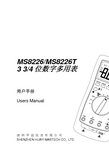
目录概述 (1)开箱检查 (1)安全信息 (2)安全要求 (3)快速开始 (5)安全符号 (5)仪表面板 (6)按键功能 (7)其它功能 (8)测量操作 (9)交直流电压测量 (9)交直流电流测量 (10)电阻测量 (11)电容测量 (12)频率和占空比测量 (13)温度测量 (14)二极管测量 (15)通断测试 (16)技术指标 (17)综合指标 (17)准确度和分辩率 (18)维护 (23)更换电池 (23)更换保险管 (24)其它 (24)RS232C串行接口 (25)概述MS8226/MS8226T是一款功能齐全、性能稳定、安全可靠性高的3 3/4位的数字多用表。
仪表使用了大规模集成电路双积分的A/D转换器,具有自动量程和手动量程,所有量程都具有过载保护功能,能测量交直流电压、交直流电流、电阻、二极管、通断测试、电容、频率、占空比和温度。
仪表采用先进的两次注塑工艺,使仪表的外壳具有更可靠的绝缘性能。
开箱检查打开包装箱取出仪表,请仔细检查下列附件是否缺少或损坏,如有缺少或损坏请立即与你的供应商联系。
z数字多用表一台z使用说明书一本z表笔一副z温度探头一个z PC接口电缆一根z软件光盘一张- 1 -IEC1010 –1过压CAT.Ⅲ,使用污染等级Ⅱ的安- 2 -安全要求为避免危及使用者的安全,在使用仪表之前请仔细阅读本使用手册,并严格遵守安全警告信息和操作说明来使用本仪表。
在测量30V以上的电压;测量10mA以上的电流;测量带电感负载的交流电力线;测量电力波动期间的交流电力线时,请要特别小心以防电击。
在每次使用仪表之前都要检查您的仪表和表笔线是否有异常或破损,如果发现任何异常情况,如表笔线磨损或断裂、外壳破裂、显示器无显示等,请立即停止使用并送修。
仪表只有和所配备的表笔线一起使用才符合安全标准的要求。
如表笔线破损时,必需更换上同样型号或者相同电气规格的表笔线。
不要使用其它未经指定或认可的保险管来更换仪表内部的保险管。
TCL100DC3-V中文资料
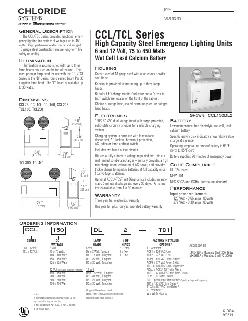
# OF HEADS 3 = Three 2 = Two 1 = One
12 Volt (Includes standard voltmeter) 150 = 150 Watt 200 = 200 Watt 300 = 300 Watt 450 = 450 Watt
12 Volt DNY = 12 Watt, Tungsten DE = 28 Watt, Tungsten DK = 25 Watt, Tungsten DG = 30 Watt, Tungsten
Battery Low maintenance, free electrolyte, wet cell, lead calcium battery
Charging system is complete with low voltage disconnect, AC lockout, brownout protection, AC indicator lamp and test switch.
Self-Diagnostics The ACCU-TEST Self-Diagnostics option conducts automatic and manual tests, and indicates real time status of the lamp, battery and charger via LED indicator lamps. Automatic tests include: Systems analysis every 10 seconds, with actual load tests performed for a 3 minute duration every 30 days. A manual tests is available from 1 to 90 minutes.
三位半数字万用表

第一章系统概述1.1 课程设计的目的与要求课程设计的主要目的,是通过电子技术的综合设计,熟悉一般电子电路综合设计过程、设计要求、完成的工作内容和具体的设计方法。
通过设计也有助于复习、巩固以往的学习模电、数电内容,达到灵活应用的目的。
在设计完成后,还要将设计的电路进行安装、调试以加强学生的动手能力。
在此过程中培养从事设计工作的整体观念。
课程设计应强调以能力培养为主,在独立完成设计任务同时注意多方面能力的培养与提高,主要包括以下方面:1、独立工作能力和创造力。
2、综合运用专业及基础知识,解决实际工程技术问题的能力。
3、查阅图书资料、产品手册和各种工具书的能力。
4、熟悉常用电子仪器操作使用和测试方法。
5、工程绘图能力。
6、写技术报告和编制技术资料的能力。
题目:设计3 1/2数字万用表具体要求:(一)根据题目,利用所学知识,通过上网或到图书馆查阅资料,设计实现数字万用表的方案,须采用中小规模集成电路、MC14433A/D转换器等电路进行设计,写出已确定方案详细工作原理,计算出参数。
(二)技术指标:1、测量直流电压1999-0001V;199.9-0.1V;19.99-0.01V;1.999-0.001V;测量交流电压1999-199V。
2、交、直流电流;3、电阻、电容;4、三位半数字显示。
1.2 方案设计与论证方案一:根据系统功能实现要求,决定控制系统采用AVR单片机,A/D转换采用其内置的10位AD、四个共阴极LED数码管。
系统除能确保实现要求的功能外,还可以方便地进行数据通讯上传,存储等扩展功能。
图1.1单片机原理图方案二:采用双积分A/D转换器MC14433,七段译码驱动器CD4511,基准电源MC1403。
图1.2MC14433原理框图方案三:由ICL7106构成的3 1/2为数字万用表原理:该系统采用ICL7106、四个共阴极LED数码管,ICL7106内部包括模拟电路(即双积分A/D转换器)、数字电路两大部分。
V30V1.0-C01说明书

本说明书使用的标识含义如下: 标识 含义 提醒在操作设备过程中需要注意的事项,不当的操作可能会导 致设置无法生效、数据丢失或者损坏设备。 对操作内容的描述进行必要的补充和说明。
注意 提示
内容简介
本说明书各章节内容安排如下: 章节 1 产品介绍 2 快速上网 3 设备管理 4 附录 内容 介绍设备的外观、包装及功能特性。 介绍通过设备上网的快速设置步骤。 介绍设备 WEB 管理页面中各功能的使用。 介绍设置电脑 IP 地址、 连接 WiFi、 常见问题解答、 有毒有害物质。
声明
声明
版权所有©2015 深圳市和为顺网络技术有限公司。保留一切权利。 未经本公司书面许可,任何单位或个人不得擅自复制、摘抄及翻译本文档部分或全部内容, 并不得以任何形式传播。 是深圳市和为顺网络技术有限公司在中国和(或)其它国家与地区的 注册商标。其它品牌和产品名称均为其相应持有人的商标或注册商标。 由于产品版本升级或其它原因,本文档内容会不定期更新。除非另有约定,本文档仅作为使 用指导,文中的所有陈述、信息和建议均不构成任何形式的担保。
2 快速上网 .................................................................................. 6
第一步:准备工作 ........................................................................................................................... 7 第二步:安装路由器 ..................................................................................................................... 10 桌面安装 ...................................................................................................................................... 10 挂壁安装 ...................................................................................................................................... 11 第三步:连接路由器 ..................................................................................................................... 14 第四步:设置上网 ......................................................................................................................... 15 步骤一:登录路由器管理页面 ................................................................................................ 15 步骤二:设置上网信息 ............................................................................................................. 16 第五步:客户端上网 ..................................................................................................................... 19
V30100PW-M34W;中文规格书,Datasheet资料
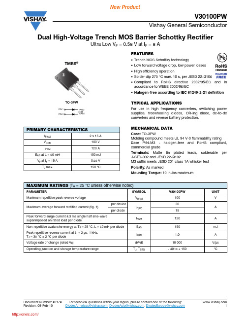
Document Number: 89178For technical questions within your region, please contact one of the following:Dual High-Voltage Trench MOS Barrier Schottky RectifierUltra Low V F = 0.58 V at I F = 8 AV30100PWVishay General SemiconductorFEATURES•Trench MOS Schottky technology•Low forward voltage drop, low power losses •High efficiency operation•Solder dip 275 °C max. 10 s, per JESD 22-B106•Compliant to RoHS directive 2002/95/EC and in accordance to WEEE 2002/96/EC•Halogen-free according to IEC 61249-2-21 definitionTYPICAL APPLICATIONSFor use in high frequency converters, switching power supplies, freewheeling diodes, OR-ing diode, dc-to-dc converters and reverse battery protection.MECHANICAL DATACase: TO-3PWMolding compound meets UL 94 V-0 flammability rating Base P/N-M3 - halogen-free and RoHS compliant,commercial gradeTerminals: Matte tin plated leads, solderable per J-STD-002 and JESD 22-B102M3 suffix meets JESD 201 class 1A whisker test Polarity: As markedMounting Torque: 10 in-lbs maximumPRIMARY CHARACTERISTICSI F(AV) 2 x 15 A V RRM 100 V I FSM120 A E AS at L = 60 mH 150 mJ V F at I F = 15 A 0.68 V T J max.150 °CMAXIMUM RATINGS (T A = 25°C unless otherwise noted)PARAMETERSYMBOL V30100PWUNIT Maximum repetitive peak reverse voltage V RRM 100V Maximum average forward rectified current (fig. 1)per device I F(AV)30A per diode15Peak forward surge current 8.3 ms single half sine-wave superimposed on rated load per diodeI FSM 120A Non-repetitive avalanche energy at T J = 25 °C, L = 60 mH per diode E AS 150mJ Peak repetitive reverse current at t p = 2 μs, 1 kHz,T J = 38 °C ± 2 °C per diode I RRM 1.0A Voltage rate of change (rated V R )dV/dt 10 000V/μs Operating junction and storage temperature rangeT J , T STG- 40 to + 150°C For technical questions within your region, please contact one of the following:Document Number: 89178V30100PWVishay General SemiconductorNotes(1)Pulse test: 300 μs pulse width, 1 % duty cycle (2)Pulse test: Pulse width ≤ 40 msRATINGS AND CHARACTERISTICS CURVES(T A = 25 °C unless otherwise noted)Fig. 1 - Forward Current Derating Curve Fig. 2 - Forward Power Loss Characteristics Per DiodeELECTRICAL CHARACTERISTICS (T A = 25°C unless otherwise noted)PARAMETER TEST CONDITIONS SYMBOL TYP.MAX.UNIT Breakdown voltageI R = 1.0 mA T J = 25 °C V BR100 (minimum)-VInstantaneous forward voltage per diodeI F = 8 AT J = 25 °CV F (1)0.64-V I F = 15 A 0.830.91I F = 8 A T J = 125 °C 0.58-I F = 15 A 0.680.76Reverse current per diodeV R = 70 VT J = 25 °C I R (2) 6.3-μA T J = 125 °C 4.4-mA V R = 100 VT J = 25 °C 22450μA T J = 125 °C1026mATHERMAL CHARACTERISTICS (T A = 25°C unless otherwise noted)PARAMETERSYMBOL V30100PWUNIT Typical thermal resistanceper diode R θJC2.0°C/Wper device1.4ORDERING INFORMATION (Example)PACKAGE PREFERRED P/N UNIT WEIGHT (g)PACKAGE CODEBASE QUANTITYDELIVERY MODETO-3PWV30100PW-M3/4W4.54W30/tubeTubeDocument Number: 89178For technical questions within your region, please contact one of the following:V30100PWVishay General SemiconductorFig. 3 - Typical Instantaneous Forward Characteristics Per Diode Fig. 4 - Typical Reverse Characteristics Per Diode Fig. 5 - Typical Junction Capacitance Per DiodeFig. 6 - Typical Transient Thermal Impedance Per DiodePACKAGE OUTLINE DIMENSIONS in inches (millimeters)Legal Disclaimer Notice VishayDisclaimerALL PRODU CT, PRODU CT SPECIFICATIONS AND DATA ARE SU BJECT TO CHANGE WITHOU T NOTICE TO IMPROVE RELIABILITY, FUNCTION OR DESIGN OR OTHERWISE.Vishay Intertechnology, Inc., its affiliates, agents, and employees, and all persons acting on its or their behalf (collectively,“Vishay”), disclaim any and all liability for any errors, inaccuracies or incompleteness contained in any datasheet or in any other disclosure relating to any product.Vishay makes no warranty, representation or guarantee regarding the suitability of the products for any particular purpose or the continuing production of any product. To the maximum extent permitted by applicable law, Vishay disclaims (i) any and all liability arising out of the application or use of any product, (ii) any and all liability, including without limitation special, consequential or incidental damages, and (iii) any and all implied warranties, including warranties of fitness for particular purpose, non-infringement and merchantability.Statements regarding the suitability of products for certain types of applications are based on Vishay’s knowledge of typical requirements that are often placed on Vishay products in generic applications. Such statements are not binding statements about the suitability of products for a particular application. It is the customer’s responsibility to validate that a particular product with the properties described in the product specification is suitable for use in a particular application. Parameters provided in datasheets and/or specifications may vary in different applications and performance may vary over time. All operating parameters, including typical parameters, must be validated for each customer application by the customer’s technical experts. Product specifications do not expand or otherwise modify Vishay’s terms and conditions of purchase, including but not limited to the warranty expressed therein.Except as expressly indicated in writing, Vishay products are not designed for use in medical, life-saving, or life-sustaining applications or for any other application in which the failure of the Vishay product could result in personal injury or death. Customers using or selling Vishay products not expressly indicated for use in such applications do so at their own risk and agree to fully indemnify and hold Vishay and its distributors harmless from and against any and all claims, liabilities, expenses and damages arising or resulting in connection with such use or sale, including attorneys fees, even if such claim alleges that Vishay or its distributor was negligent regarding the design or manufacture of the part. Please contact authorized Vishay personnel to obtain written terms and conditions regarding products designed for such applications.No license, express or implied, by estoppel or otherwise, to any intellectual property rights is granted by this document or by any conduct of Vishay. Product names and markings noted herein may be trademarks of their respective owners.Material Category PolicyVishay Intertechnology, Inc. hereb y certifies that all its products that are identified as RoHS-Compliant fulfill the definitions and restrictions defined under Directive 2011/65/EU of The European Parliament and of the Council of June 8, 2011 on the restriction of the use of certain hazardous substances in electrical and electronic equipment (EEE) - recast, unless otherwise specified as non-compliant.Please note that some Vishay documentation may still make reference to RoHS Directive 2002/95/EC. We confirm that all the products identified as being compliant to Directive 2002/95/EC conform to Directive 2011/65/EU.Revision: 12-Mar-121Document Number: 91000分销商库存信息:VISHAY-GENERAL-SEMICONDUCTOR V30100PW-M3/4W。
GT30L32S4W规格书V1.1I_A
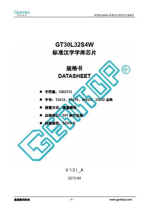
8.1 GB2312 1 区字符 (846 字符) ........................................................................................................................................................27 8.2 8×16 点国标扩展字符(126 字符) .............................................................................................................................................30 8.3 8×16 点特殊字符(64 字符) .......................................................................................................................................................31
- 1、下载文档前请自行甄别文档内容的完整性,平台不提供额外的编辑、内容补充、找答案等附加服务。
- 2、"仅部分预览"的文档,不可在线预览部分如存在完整性等问题,可反馈申请退款(可完整预览的文档不适用该条件!)。
- 3、如文档侵犯您的权益,请联系客服反馈,我们会尽快为您处理(人工客服工作时间:9:00-18:30)。
V30100C, VF30100C, VB30100C & VI30100CVishay General SemiconductorDocument Number: 89010For technical questions within your region, please contact one of the following:Dual High-Voltage Trench MOS Barrier Schottky RectifierUltra Low V F = 0.455 V at I F = 5 AFEATURES•Trench MOS Schottky technology •Low forward voltage drop, low power losses •High efficiency operation •Low thermal resistance•Meets MSL level 1, per J-STD-020, LF maximum peak of 245 °C (for TO-263AB package) •Solder bath temperature 275 °C maximum, 10 s,per JESD 22-B106 (for TO-220AB, ITO-220AB and TO-262AA package) •Compliant to RoHS directive 2002/95/EC and in accordance to WEEE 2002/96/EC TYPICAL APPLICATIONSFor use in high frequency converters, switching power supplies, freewheeling diodes, OR-ing diode, dc-to-dc converters and reverse battery protection.MECHANICAL DATACase: TO-220AB, ITO-220AB, TO-263AB and TO-262AAMolding compound meets UL 94 V-0 flammability ratingBase P/N-E3 - RoHS compliant, commercial grade Terminals: Matte tin plated leads, solderable per J-STD-002 and JESD 22-B102E3 suffix meets JESD 201 class 1A whisker test Polarity: As markedMounting Torque: 10 in-lbs maximumPRIMARY CHARACTERISTICSI F(AV) 2 x 15 A V RRM 100 V I FSM 160 A V F at I F = 15 A 0.63 V T J max.150 °C12312KMAXIMUM RATINGS (T A = 25°C unless otherwise noted)PARAMETER S YMBOL V30100C VF30100C VB30100C VI30100C UNITMaximum repetitive peak reverse voltage V RRM 100V Maximum average forward rectified current (fig. 1)per device per diodeI F(AV)3015A Peak forward surge current 8.3 ms single half sine-wave superimposed on rated load per diode I FSM 160ANon-repetitive avalanche energy at T J = 25 °C, L = 60 mH per diodeE AS 210mJ Peak repetitive reverse current at t p = 2 µs, 1 kHz, T J = 38 °C ± 2 °C per diode I RRM 1.0A Voltage rate of change (rated V R )dV/dt 10 000V/µs Isolation voltage (ITO-220AB only)from terminal to heatsink t = 1 minV AC 1500V Operating junction and storage temperature range T J , T STG- 40 to + 150°CV30100C, VF30100C, VB30100C & VI30100CVishay General Semiconductor For technical questions within your region, please contact one of the following:Document Number: 89010Notes(1) Pulse test: 300 µs pulse width, 1 % duty cycle (2) Pulse test: Pulse width ≤ 40 msRATINGS AND CHARACTERISTICS CURVES (T A = 25 °C unless otherwise noted)ELECTRICAL CHARACTERISTICS (T A = 25°C unless otherwise noted)PARAMETER TEST CONDITIONS SYMBOL TYP.MAX.UNITBreakdown voltageI R = 1.0 mA T A = 25 °C V BR100 (minimum)-VInstantaneous forward voltage per diode (1)I F = 5 A I F = 7.5 A I F = 15 A T A = 25 °CV F0.5160.5760.734--0.80I F = 5 A I F = 7.5 A I F = 15 A T A = 125 °C 0.4550.5220.627--0.68Reverse current per diode (2)V R = 70 VT A = 25 °C T A = 125 °C I R7.28.0--µA mA V R = 100 VT A = 25 °C T A = 125 °C652050035µA mA THERMAL CHARACTERISTICS (T A = 25°C unless otherwise noted)PARAMETER S YMBOL V30100CVF30100CVB30100CVI30100CUNITTypical thermal resistance per diodeR θJC 2.55.52.52.5°C/WORDERING INFORMATION (Example)PACKAGE PREFERRED P/N UNIT WEIGHT (g)PACKAGE CODEBASE QUANTITYDELIVERY MODETO-220AB V30100C-E3/4W 1.884W 50/tube Tube ITO-220AB VF30100C-E3/4W 1.754W 50/tube Tube TO-263AB VB30100C-E3/4W 1.394W 50/tube Tube TO-263AB VB30100C-E3/8W 1.398W 800/reel Tape and reelTO-262AAVI30100C-E3/4W1.464W50/tubeTubeFigure 1. Forward Current Derating CurveFigure 2. Forward Power Loss Characteristics Per DiodeV30100C, VF30100C, VB30100C & VI30100CVishay General SemiconductorDocument Number: 89010For technical questions within your region, please contact one of the following:Figure 3. Typical Instantaneous Forward Characteristics Per Diode Figure 4. Typical Reverse Characteristics Per Diode Figure 5. Typical Junction CapacitanceFigure 6. Typical Transient Thermal Impedance Per DiodeFigure7. Typical Transient Thermal Impedance Per DiodeV30100C, VF30100C, VB30100C & VI30100CVishay General Semiconductor For technical questions within your region, please contact one of the following:Document Number: 89010PACKAGE OUTLINE DIMENSIONS in inches (millimeters)Legal Disclaimer Notice VishayDisclaimerALL PRODU CT, PRODU CT SPECIFICATIONS AND DATA ARE SU BJECT TO CHANGE WITHOU T NOTICE TO IMPROVE RELIABILITY, FUNCTION OR DESIGN OR OTHERWISE.Vishay Intertechnology, Inc., its affiliates, agents, and employees, and all persons acting on its or their behalf (collectively,“Vishay”), disclaim any and all liability for any errors, inaccuracies or incompleteness contained in any datasheet or in any other disclosure relating to any product.Vishay makes no warranty, representation or guarantee regarding the suitability of the products for any particular purpose or the continuing production of any product. To the maximum extent permitted by applicable law, Vishay disclaims (i) any and all liability arising out of the application or use of any product, (ii) any and all liability, including without limitation special, consequential or incidental damages, and (iii) any and all implied warranties, including warranties of fitness for particular purpose, non-infringement and merchantability.Statements regarding the suitability of products for certain types of applications are based on Vishay’s knowledge of typical requirements that are often placed on Vishay products in generic applications. Such statements are not binding statements about the suitability of products for a particular application. It is the customer’s responsibility to validate that a particular product with the properties described in the product specification is suitable for use in a particular application. Parameters provided in datasheets and/or specifications may vary in different applications and performance may vary over time. All operating parameters, including typical parameters, must be validated for each customer application by the customer’s technical experts. Product specifications do not expand or otherwise modify Vishay’s terms and conditions of purchase, including but not limited to the warranty expressed therein.Except as expressly indicated in writing, Vishay products are not designed for use in medical, life-saving, or life-sustaining applications or for any other application in which the failure of the Vishay product could result in personal injury or death. Customers using or selling Vishay products not expressly indicated for use in such applications do so at their own risk and agree to fully indemnify and hold Vishay and its distributors harmless from and against any and all claims, liabilities, expenses and damages arising or resulting in connection with such use or sale, including attorneys fees, even if such claim alleges that Vishay or its distributor was negligent regarding the design or manufacture of the part. Please contact authorized Vishay personnel to obtain written terms and conditions regarding products designed for such applications.No license, express or implied, by estoppel or otherwise, to any intellectual property rights is granted by this document or by any conduct of Vishay. Product names and markings noted herein may be trademarks of their respective owners.Material Category PolicyVishay Intertechnology, Inc. hereb y certifies that all its products that are identified as RoHS-Compliant fulfill the definitions and restrictions defined under Directive 2011/65/EU of The European Parliament and of the Council of June 8, 2011 on the restriction of the use of certain hazardous substances in electrical and electronic equipment (EEE) - recast, unless otherwise specified as non-compliant.Please note that some Vishay documentation may still make reference to RoHS Directive 2002/95/EC. We confirm that all the products identified as being compliant to Directive 2002/95/EC conform to Directive 2011/65/EU.Revision: 12-Mar-121Document Number: 91000分销商库存信息:VISHAY-GENERAL-SEMICONDUCTOR V30100C-E3/4W。