1520A-30-1.0A中文资料
uscar-30 中文版
4 一般要求概述 ................................................................................................................. 錯誤! 尚未定義書籤。
4.1 持續紀錄................................................................................................................. 錯誤! 尚未定義書籤。 4.2 樣品文件................................................................................................................. 錯誤! 尚未定義書籤。 4.3 樣品尺寸................................................................................................................. 錯誤! 尚未定義書籤。 4.4 默認測試公差......................................................................................................... 錯誤! 尚未定義書籤。 4.5 默認測試條件......................................................................................................... 錯誤! 尚未定義書籤。 4.6 設備......................................................................................................................... 錯誤! 尚未定義書籤。 4.7 測量方法................................................................................................................. 錯誤! 尚未定義書籤。 4.8 測量重復性&標准性............................................................................................. 錯誤! 尚未定義書籤。 4.9 一致性規定............................................................................................................. 錯誤! 尚未定義書籤。 4.10 樣品處置................................................................................................................. 錯誤! 尚未定義書籤。 4.11 零件耐久性 E.......................................................................................................... 錯誤! 尚未定義書籤。
AP1520

PWM Control 2A Step-Down ConverterFeatures- Input voltage: 3.6V to 23V. - Output voltage: 0.8V to V CC .- Duty ratio: 0% to 100% PWM control - Oscillation frequency: 300KHz typ.- Soft-start, Current Limit, Enable function - Thermal Shutdown function- Built-in internal SW P-channel MOS - SOP-8L Pb-Free Package.Applications- PC Motherboard - LCD Monitor - Graphic Card- DVD-Video Player - Telecom Equipment - ADSL Modem- Printer and other Peripheral Equipment - Microprocessor core supply - Networking power supplyGeneral DescriptionAP1520 consists of step-down switching regulator with PWM control. These devices include a reference voltage source, oscillation circuit, error amplifier, internal PMOS and etc.AP1520 provides low-ripple power, high efficiency, and excellent transient characteristics. The PWM control circuit is able to vary the duty ratio linearly from 0 up to 100%. This converter also contains an error amplifier circuit as well as a soft-start circuit that prevents overshoot at startup. An enable function, an over current protect function and a short circuit protect function are built inside, and when OCP or SCP happens, the operation frequency will be reduced from 300KHz to 30KHz. Also, an internal compensation block is built in to minimum external component count.With the addition of an internal P-channel Power MOS, a coil, capacitors, and a diode connected externally, these ICs can function as step-down switching regulators. They serve as ideal power supply units for portable devices when coupled with the SOP–8L mini-package, providing such outstanding features as low current consumption. Since this converter can accommodate an input voltage up to 23V, it is also suitable for the operation via an AC adapter.Pin AssignmentsOutput OCSET Output EN Vss VssV CCPin DescriptionsName Pin Description FB 1 Feedback pin.EN 2Power-off pinH: Normal operation (Step-down operation)L: Step-down operation stopped (All circuits deactivated)OCSET 3Add an external resistor to setmax output current.V CC 4 IC power supply pinOutput 5、6Switch Pin. Connect external inductor/diode here. Minimizetrace area at this pin to reduce EMI. V SS7、8GND PinPWM Control 2A Step-Down ConverterOrdering InformationAP1520X XPackage PackingS: SOP-8L Blank : TubeA : TapingBlock DiagramVccAbsolute Maximum RatingsSymbol Parameter Rating UnitV CC V CC Pin Voltage V SS - 0.3 to V SS + 25 VV FB Feedback Pin Voltage V SS - 0.3 to V CC V V EN EN Pin Voltage V SS - 0.3 to V IN + 0.3 VPinVoltage V SS - 0.3 to V IN + 0.3 V V OUTPUT SwitchP D Power Dissipation Internally limited mWT OPR Operating Temperature Range -20 to +125 o CT STG Storage Temperature Range -40 to +150 o CCaution: The absolute maximum ratings are rated values exceeding which the product could suffer physical damage. These values must therefore not be exceeded under any conditions.PWM Control 2A Step-Down ConverterElectrical Characteristics (V IN = 12V, T a =25°C , unless otherwise specified)Symbol Parameter Conditions Min.Typ. Max.Unit V IN Input Voltage -- 3.6 - 23 V V FB Feedback Voltage I OUT =0.1A 0.7840.8 0.816V I FB Feedback Bias Current I OUT =0.1A - 0.1 0.5 µA I SW Switch Current -- 2.5 - - AI SSS Current ConsumptionDuring Power offV EN =0V - 10 - µA∆V OUT/V OUT Line Regulation V IN = 5V~23V-1 2 % ∆V OUT/V OUT Load Regulation I OUT =0.1 to 2A - 0.2 0.5 %f OSC Oscillation Frequency Measure waveform at SW pin 240 300 360 KHzf OSC1Frequency of Current Limitor Short Circuit ProtectMeasure waveform at SW pin 10 - - KHz V SH Evaluate oscillation at SW pin 2.0 - -V SL EN Pin Input Voltage Evaluate oscillation stop at SW pin - - 0.8 V I SH -- - 20 - µA I SL EN Pin Input Leakage Current -- - -10 - µA I OCSET OCSET Pin Bias Current -- 75 90 105 µA T SS Soft-Start Time -- 0.3 1 2 msV IN =5V, V FB =0V - 110 150R DSON Internal MOSFET RdsonV IN =12V, V FB =0V - 70 100 m ΩEFFI EfficiencyV IN = 12V, V OUT = 5VI OUT = 2A- 92 - % θJA Thermal Resistance Junction-to-Ambient- 65 - oC/WTypical Application CircuitOUTV Note: V OUT = V FB x (1+R A /R B ) R B =0.7K~5K ohmV IN =12V, I MAX =2AV OUT 2.5V 3.3V 5V L1 Value22uH 27uH 33uHPWM Control 2A Step-Down Converter Typical Performance CharacteristicsPWM Control 2A Step-Down ConverterTypical Performance Characteristics (Continued)AP1520 Vout Ripple(Vin=12V; Vout=3.3V; Iout=0.1A) AP1520 Vout Ripple(Vin=12V; Vout=3.3V; Iout=2A)Test CircuitPWM Control 2A Step-Down ConverterFunction DescriptionPWM ControlThe AP1520 consists of DC/DC converters that employ a pulse-width modulation (PWM) system. In converters of the AP1520, the pulse width varies in a range from 0 to 100%, according to the load current. The ripple voltage produced by the switching can easily be removed through a filter because the switching frequency remains constant. Therefore, these converters provide a low-ripple power over broad ranges of input voltage and load current.Under Voltage LockoutThe under voltage lockout circuit of the AP1520 assures that the high-side MOSFET driver outputs remain in the off state whenever the supply voltage drops below 3.3V. Normal operation resumes once V CC rises above 3.5V.R DS(ON) Current LimitingThe current limit threshold is setting by the external resistor connecting from V CC supply to OCSET. The internal 100uA sink current crossing the resistor sets the voltage at the pin of OCSET. When the PWM voltage is less than the voltage at OCSET, an over-current condition is triggered.R I R I OCSET OCSET DS(ON)LOAD ×=×See above formula for setting the current limit value.Marking Information( Top View )LogoPart no.ID code: internal Year: "01" =2001 "02" =2002Xth week: 01~52~AP1520YY WW XPWM Control 2A Step-Down ConverterPackage InformationPackage Type: SOP-8LDimensions In Millimeters Dimensions In InchesSymbolMin. Nom. Max. Min. Nom. Max.A 1.40 1.60 1.75 0.055 0.063 0.0690.040 - 0.100A1 0.10 - 0.25A2 1.30 1.45 1.50 0.051 0.057 0.059B 0.33 0.41 0.51 0.013 0.016 0.020C 0.19 0.20 0.25 0.0075 0.008 0.010D 4.80 5.05 5.30 0.189 0.199 0.209E 3.70 3.90 4.10 0.146 0.154 0.161e - 1.27 - - 0.050 -H 5.79 5.99 6.20 0.228 0.236 0.244L 0.38 0.71 1.27 0.015 0.028 0.050y - - 0.10 - - 0.004θ0O - 8O0O - 8O。
30V20A电源说明书

高精度直流稳压电源使用说明书(RYI-1510 RYI-1520 RYI-3010 RYI-3020 RYI3030)一、概述PYI―1510A、PYI―3020A型高精度直流稳压电源,是采用截止式保护电路,保护速度快,对电源及负载的短路和过流(≥10.2A、≥20.2A)能及时加以保护,消除短路及过流故障后从新启动一下电源开关即可恢复正常工作。
RYI-3010A、RYI3005A型为高精度恒压、恒流型直流稳压电源,特点为精度高、可靠性强。
适用于科技产品开发、实验室、电子生产线及移动电话、无线寻呼机维修使用。
二、参数规格2-1、额定工作条件及外形尺寸:电源电压220V±10%50/60HZ(根据要求也可以定在110V±10%50/60HZ)工作条件温度:-10℃-40℃相对湿度:<90%储存条件温度: -20℃-80℃相对湿度:<80%外形尺寸:165×118×195(mm)、165×118×230 mm2-2、稳压工作状态:(1)输出电压从0到标称值之间连续可调(2)电压稳定度电源稳定度≤0.01%+2mV负载稳定度≤0.01%+2mV(3)恢复时间≤100uS(4)纹波噪声≤1MVRMS(有效值)(5)温度系数≤300PPM/℃(6)保护启动电流大于最大标称值的10%2-3、恒流状态(1)输出电流在0到称值之间连续可调(2)电流、负载变化稳定度≤0.2%+3mA(3)纹波和噪声:≤3mArms三、使用说明3-1、注意事项:(1)交流输入交流输入应为220V±10%50HZ(如果是110V±10%60HZ在机箱后面会标明)(2)绝缘请勿在坏境温度超过40℃的地方使用,散热器位于仪器的后部,应留有足够的空间,以利于散热。
散热器温度可达100℃,长时间使用时,请不要用手触到散热器。
(3)输出电压过冲限制当开关电源时,输出端之间的电压不超过预置3-2、操作方法:(1)接上电源。
交流接触器AX09-30-01.
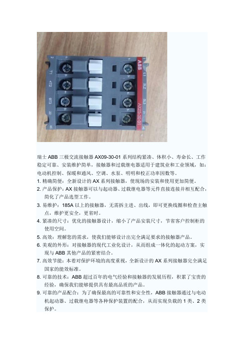
瑞士ABB三极交流接触器AX09-30-01系列结构紧凑、体积小、寿命长、工作稳定可靠、安装维护简单,接触器和过载继电器适用于建筑业和工业领域,如:电动机控制、保暖和通风、空调、水泵、明明和校正功率因数等。
1. 精确简便:全新设计的AX系列接触器,使现场的安装和使用更加简便。
2. 产品保护:AX接触器可以与起动器、过载继电器等元件直接连接并相互配合,简化了产品选型工作。
3. 易维护:185A以上的接触器,无需拆主进、出线,即可更换线圈和检查主触点,维护更安全,更省时。
4. 紧凑的尺寸:优化的接触器设计,缩小了产品安装尺寸,节省客户控制柜的使用空间。
5. 高效:理解您的需求,使我们能够设计出完全满足要求的接触器产品。
6. 美观的外形:对接触器的现代工业化设计,从而组成一体化的起动方案,实现与ABB其他产品的紧密结合。
7. 高效节能:本着对保护环境的高度重视,全新设计的AX系列接触器完全满足国家的能效标准。
8. 可靠的技术:ABB超过百年的电气经验和接触器的发展历程,积累了宝贵的经验,确保我们能够提供具有最高品质的产品。
9. 可靠的产品配合:为了确保最高的可靠性和安全性,ABB接触器通过与电动机起动器、过载继电器等各种保护装置的配合,从而实现负载的1类、2类保护。
10. 材质:为了减少环境的影响,我们选择符合ROHS指令和国内有关规定的产品材质。
11. 产品认证:符合IEC60947-4-1、GB14048.4。
具有CCC、CE、CCS认证保顺0577********.新华社北京10月3日电(记者许晟)工业和信息化部近日发布数据,今年前8个月,电子信息产业500万元以上项目完成固定资产投资额8573.5亿元,同比增长15.9%,高于同期工业投资7.2个百分点。
数据显示,今年前8个月,东部、西部地区电子信息产业投资增速较快,中部和东北地区增速低于全国平均水平。
其中北京增长61.4%,福建增长48.2%,广东增长40.6%;湖南则持续负增长,东北地区完成投资367.1亿元,同比增长5.5%,青海增长91.3%,增速居全国首位。
LH1522资料

LH1531, LH1532, LH1544 2
A. LED Voltage vs. Temperature
1.6
1.5 IF = 20 mA
1.4
IF = 50 mA
LED FORWARD VOLTAGE (V)
1.3
1.2 IF = 1 mA
IF = 2 mA 1.1
IF = 5 mA
1.0
IF = 10 mA
40
IFON = 4 mA
20 LH1L5H3212532
0
–40 –20
0
20
40
60
80
AMBIENT TEMPERATURE (°C)
1
Electrical Characteristics TA=25°C Minimum and maximum values are testing require-
–40 –20
0
20
40
60
80
AMBIENT TEMPERATURE (°C)
C. LED Current for Switch Turn-On vs. Temperature
LED FORWARD CURRENT FOR SWITCH TURN-ON (%) NORMALIZED TO 25 °C
Parameter
Symbol Test Conditions
Values
LH1531
LH1532
LH1544 Units
LED Forward Current for Switch Turn-on
INPUT
LED Forward Current for Switch Turn-off
MAX15301数据手册中文版

MAX15301是一个全功能,高效,数字化的点负载(POL)操纵器与先进的电源治理和遥测功能与PID 为基础的数字电源稳压器,MAX15301采纳Maxim拥有专利的Intune的™自动补偿,状态空间操纵算法。
Intune 的操纵律是有效的小信号和大信号响应,占占空比饱和度的阻碍。
这排除需要用户以确信和设置的阈值从线性转换到非线性模式。
这些能力在快速环路的瞬态响应,并减少输出电容器的数量相较,竞争的模拟和数字操纵器。
MAX15301包括多种功能,以优化效率。
内部开关BabyBuck的稳压器可产生栅极驱动器和内部偏置电源,低功耗的操纵器。
一种先进的,高效率的MOSFET的栅极驱动器,具有自适应非重叠按时,而持续调整的高侧和低侧的按时和驱动电压的全范围内的电压,电流和温度,以尽可能减少开关损耗。
MAX15301设计最终客户的设计环境的初衷。
上的PMBus™兼容的串行总线接口进行通信的监控器监控和故障治理。
全套的电源治理功能,无需复杂和昂贵的测序和监控IC。
大体的DC-DC转换操作,可设置通过引脚搭接,并非需要用户配置固件。
这使得电源子系统的快速进展前完成板级系统的工程。
Maxim提供支持的硬件和软件配置MAX15301 ,MAX15301可在32引线,5mm×5mm TQFN封装,工作在-40°C至+85°C的温度范围内。
特点:的自动补偿功能能够确保稳固,同时优化瞬态性能2.在快速瞬态响应减少输出电容的非线性补偿结果3.差分远端电压传感许诺±1%V OUT精度在整个温度范围内(-40°C至+85°C)接口用于配置,操纵和监测5.支持电压定位6.提高效率(自适应非重叠时序驱动器)至14V的宽输入电压范围8.高效片上BabyBuck稳压器的自偏置9.输出电压范围从到10.进入预偏置输出启动11.可配置的软启动和软停止时刻12.固定工作频率同步(300kHz至1MHz)13.灵活的排序和故障治理14.引脚手动跳线配置(输出电压,从机地址,开关频率,电流限制)15.能够快速原型图表典型工作电路引脚名字功能1SYNC外部开关频率同步输入端。
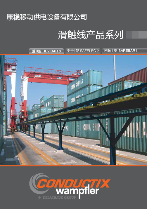
康稳(武汉汉发)滑触线样本
加强型提挂夹STRENGTHENED HANGER CLAMPS
类型
部件号 重量(KG)
四孔加强 提挂件
396007
1.17
四孔中间加 强紧固夹
396011
1.79
三孔加强 提挂件
396012
1.01
三孔中间加 强紧固夹
345016
1.47Βιβλιοθήκη 每极滑触线之间的定位中心 距是50mm。
396011
396007
04
重Ⅲ型 HEVIBAR 3 安全滑触线 630-1250A系列
滑触线 CONDUCTOR BARS
额定电流
标准型相线(橙色) 标准型地线(绿色) 中等耐热型(红色) 重量(Kg)
630A
345102 345123 345104 8.4
800A
345205 345249 345229 9.8
1000A
◆ 最大允许电压降; ◆ 环境温度、环境外在条件(灰尘、沿海、潮湿、酸雾)
电压降的计算:
三相交流电:△U= 3×I×D×Z 单相交流电:△U=2×I×D×Z 直 流 电:△U=2×I×D×Z
△U%=(△U×100)/Un
其中: Un=电压(伏) △U=电压降(伏) I=最大电流 D=供电点与取电点之间的距离(米) R=滑触线导体的电阻(欧姆/米) Z=滑触线导体的电抗(欧姆/米)
1 标准型相线
-346240-
2
3
供电接头 POWER FEEDS
额定电流
标准型相线(橙色) 标准型地线(绿色) 中等耐热型(红色) 重量(KG)
630A/800A
346250 346251 346116
0.96
FGA15N120AN中文资料

I CES Collector Cut-Off Current V CE = V CES, V GE = 0V----3mA I GES G-E Leakage Current V GE = V GES, V CE = 0V ----± 100nAOn CharacteristicsV GE(th)G-E Threshold Voltage I C = 15mA, V CE = V GE 3.5 5.57.5VV CE(sat)Collector to EmitterSaturation VoltageI C = 15A, V GE = 15V-- 2.4 3.2VI C = 15A, V GE = 15V,T C = 125°C-- 2.9--VI C = 24A, V GE = 15V-- 3.0--VDynamic CharacteristicsC ies Input Capacitance VCE = 30V, V GE = 0V,f = 1MHz --1150--pFC oes Output Capacitance--120--pF C res Reverse Transfer Capacitance--56--pFSwitching Characteristicst d(on)Turn-On Delay TimeV CC = 600 V, I C = 15A,R G = 20Ω, V GE = 15V,Inductive Load, T C = 25°C --90--nst r Rise Time--70--ns t d(off)Turn-Off Delay Time--310--ns t f Fall Time--60120ns E on Turn-On Switching Loss-- 3.27 4.9mJ E off Turn-Off Switching Loss--0.60.9mJ E ts TotalSwitchingLoss-- 3.68 5.8mJt d(on)Turn-On Delay TimeV CC = 600 V, I C = 15A,R G = 20Ω, V GE = 15V,Inductive Load, T C = 125°C --80--nst r Rise Time--60--ns t d(off)Turn-Off Delay Time--310--ns t f Fall Time--50--ns E on Turn-On Switching Loss-- 3.41--mJ E off Turn-Off Switching Loss--0.84--mJ E ts TotalSwitchingLoss-- 4.25--mJQ g Total Gate ChargeV CE = 600 V, I C = 15A,V GE = 15V --120180nCQ ge Gate-Emitter Charge--914nC Q gc Gate-Collector Charge--6395nC L e Internal Emitter Inductance Measured 5mm from PKG--14--nHFGA15N120ANDISCLAIMERFAIRCHILD SEMICONDUCTOR RESERVES THE RIGHT TO MAKE CHANGES WITHOUT FURTHER NOTICE TO ANY PRODUCTS HEREIN TO IMPROVE RELIABILITY, FUNCTION OR DESIGN. FAIRCHILD DOES NOT ASSUME ANY LIABILITY ARISING OUT OF THE APPLICATION OR USE OF ANY PRODUCT OR CIRCUIT DESCRIBED HEREIN;NEITHER DOES IT CONVEY ANY LICENSE UNDER ITS PATENT RIGHTS, NOR THE RIGHTS OF OTHERS.LIFE SUPPORT POLICYFAIRCHILD’S PRODUCTS ARE NOT AUTHORIZED FOR USE AS CRITICAL COMPONENTS IN LIFE SUPPORT DEVICES OR SYSTEMS WITHOUT THE EXPRESS WRITTEN APPROVAL OF FAIRCHILD SEMICONDUCTOR CORPORATION.As used herein:1. Life support devices or systems are devices or systems which, (a) are intended for surgical implant into the body,or (b) support or sustain life, or (c) whose failure to perform when properly used in accordance with instructions for use provided in the labeling, can be reasonably expected to result in significant injury to the user.2. A critical component is any component of a life support device or system whose failure to perform can be reasonably expected to cause the failure of the life support device or system, or to affect its safety or effectiveness.PRODUCT STATUS DEFINITIONS Definition of TermsDatasheet Identification Product Status DefinitionAdvance InformationFormative or In Design This datasheet contains the design specifications for product development. Specifications may change in any manner without notice.PreliminaryFirst ProductionThis datasheet contains preliminary data, andsupplementary data will be published at a later date.Fairchild Semiconductor reserves the right to make changes at any time without notice in order to improve design.No Identification Needed Full ProductionThis datasheet contains final specifications. Fairchild Semiconductor reserves the right to make changes at any time without notice in order to improve design.Obsolete Not In ProductionThis datasheet contains specifications on a product that has been discontinued by Fairchild semiconductor.The datasheet is printed for reference information only.TRADEMARKSThe following are registered and unregistered trademarks Fairchild Semiconductor owns or is authorized to use and is not intended to be an exhaustive list of all such trademarks.FACT Quiet Series™FAST ®FASTr™FRFET™GlobalOptoisolator™GTO™HiSeC™I 2C™ImpliedDisconnect™ISOPLANAR™LittleFET™MICROCOUPLER™MicroFET™MicroPak™MICROWIRE™MSX™MSXPro™OCX™OCXPro™OPTOLOGIC ®OPTOPLANAR™PACMAN™POP™Power247™PowerTrench ®QFET ®QS™QT Optoelectronics™Quiet Series™RapidConfigure™RapidConnect™SILENT SWITCHER ®SMART START™SPM™Stealth™SuperSOT™-3SuperSOT™-6SuperSOT™-8SyncFET™TinyLogic ®TINYOPTO™TruTranslation™UHC™UltraFET ®VCX™ACEx™ActiveArray™Bottomless™CoolFET™CROSSVOLT ™DOME™EcoSPARK™E2CMOS™EnSigna™FACT™Across the board. Around the world.™The Power Franchise™Programmable Active Droop™。
- 1、下载文档前请自行甄别文档内容的完整性,平台不提供额外的编辑、内容补充、找答案等附加服务。
- 2、"仅部分预览"的文档,不可在线预览部分如存在完整性等问题,可反馈申请退款(可完整预览的文档不适用该条件!)。
- 3、如文档侵犯您的权益,请联系客服反馈,我们会尽快为您处理(人工客服工作时间:9:00-18:30)。
152010-TAP DIP/SMD DELAY LINE T D /T R = 5(SERIES 1520)FEATURES PACKAGES1413121110981234567GNDT1T3T5T6T8T10IN N/C T2 T4 T7 T9 GND• 10 taps of equal delay increment IN Signal Input T1-T10Tap Outputs GND GroundNote:Standard pinout shownOther pinouts available• Delays to 1000ns • Low profile• Epoxy encapsulated• Meets or exceeds MIL-D-23859CFUNCTIONAL DESCRIPTIONThe 1520-series device is a fixed, single-input, ten-output, passive delay line. The signal input (IN) is reproduced at the outputs (T1-T10) in equal increments. The delay from IN to T10 (T D ) and the characteristic impedance of the line (Z) aredetermined by the dash number. The rise time (T R ) of the line is 20% of T D , and the 3dB bandwidth is given by 1.75 / T D . The device is available in a 14-pin DIP (1520) or a 14-pin SMD (1520S), and a wide range of pinouts may be specified.Part numbers are constructed according to the scheme shown at right. For example, 1520C-101-500B is a 290 mil DIP, 100ns, 50Ω delay line with pinout code B. Similarly, 1520SB-201-251 is a 240 mil SMD, 200ns, 250Ω delay line with standard pinout.DELAY TIMEExpressed in nanoseconds (ns)First two digits are significant figures Last digit specifies # of zeros to followIMPEDANCEExpressed in nanoseconds (ns)First two digits are significant figures Last digit specifies # of zeros to followPINOUT CODESee TableOmit for STD pinoutMOUNTING HEIGHT CODESee Table PART NUMBER CONSTRUCTION1520(S)m - xxx - zzz pSERIES SPECIFICATIONSDELAY SPECIFICATIONST D T I T R ATTENUATION (%) TYPICAL (ns) (ns) (ns) Z=50Ω Z =100Ω Z=200ΩZ=300ΩZ=500Ω10 1.0 3.0 3 5 N/A N/A N/A 20 2.0 5.5 3 5 5 N/A N/A 30 3.0 6.5 3 5 5 N/A N/A 40 4.0 8.0 3 5 5 5 N/A 50 5.0 10.0 3 5 5 5 7 60 6.0 12.0 3 5 5 5 7 75 7.5 15.0 3 5 5 5 7 100 10.0 20.0 3 5 5 7 7 120 12.0 24.0 3 5 6 7 8 150 15.0 30.0 3 5 6 7 8 180 18.0 36.0 4 5 6 7 8 200 20.0 40.0 4 5 6 7 8 220 22.0 44.0 4 5 6 7 8 250 25.0 50.0 4 5 6 7 8 300 30.0 60.0 N/A 5 8 10 10 375 37.5 75.0 N/A 7 8 10 10 500 50.0 100.0N/A 8 10 12 12 600 60.0 120.0N/A N/A N/A 15 15 750 75.0 150.0N/A N/A N/A 15 20 1000 100.0 200.0N/A N/A N/A N/A 20Notes: T I represents nominal tap-to-tap delay increment Tolerance on T D = ±5% or ±2ns, whichever is greater Tolerance on T I = ±5% or ±1ns, whichever is greater “N/A” indicates that delay is not available at this Z• Dielectric breakdown: 50 Vdc • Distortion @ output: 10% max. • Operating temperature: -55°C to +125°C • Storage temperature: -55°C to +125°C •Temperature coefficient: 100 PPM/°CPINOUT CODESCODE IN T1 T2 T3 T4 T5 T6 T7 T8 T9T10GND STD 14 2 12 3 11 4 5 10 6 9 7 1,8 A 1 2 13 3 12 4 10 5 9 6 7 14 B 2 3 4 5 6 7 9 10 11 12131,14 C 7 9 6 10 5 11 12 3 13 2 141,8 D 1 13 2 12 3 11 4 10 5 9 6 7,8,14E 2 3 4 5 6 7,8 9 10 11 12131,14 F 1 13 2 12 3 11 4 10 5 9 6 7 G 2 13 3 12 4 11 5 10 6 9 7 8,14 H 2 3 4 12 6 7 9 10 11 1213 1 I 1 13 2 12 3 11 5 10 6 9 7 8,14 J 1 2 13 3 12 4 10 5 9 6 7 8,14 K 1 2 3 4 5 6 12 11 10 9 8 7 L 13 12 11 10 9 7,8 6 5 4 3 2 1,14 N 1 2 3 4 5 6 10 11 12 13147 P 1 13 3 12 4 11 5 10 6 9 7 8,14 T 1 2 3 4 5 6 9 10 11 12137,14 U 2 3 4 5 6 8 9 10 11 12131,7 V 2 3 4 5 6 8 9 10 11 1213 1 W 1 13 2 12 3 11 4 10 5 9 6 7,14 Z 1 13 3 12 4 11 5 10 6 9 8 72004 Data Delay DevicesDoc #97028DATA DELAY DEVICES, INC.15/5/043 Mt. Prospect Ave. Clifton, NJ 070131520MOUNTING HEIGHT CODESCODE HEIGHT(MAX) DIP SMDA 0.187 YesNoB 0.240 YesYesC 0.290 YesYes FUNCTIONAL DIAGRAMGNDIN T10T1T2T3T4T6T7T8T9T5GNDNote:Codes A and B are notfor all values of T DContact technical staff foavailabler detailsPACKAGE DIMENSIONS1520-xx (DIP)each .100±.010Non-Accumulative1520S-xx (Gull-Wing)Doc #97028DATA DELAY DEVICES, INC. 25/5/04 Tel: 973-773-2299 Fax: 973-773-9672 1520PASSIVE DELAY LINE TEST SPECIFICATIONSTEST CONDITIONSINPUT: OUTPUT:Ambient Temperature: 25o C ± 3oC R load : 10M Ω Input Pulse: High = 3.0V typical C load : 10pf Low = 0.0V typical Threshold: 50% (Rising & Falling) Source Impedance: 50Ω Max. Rise/Fall Time: 3.0 ns Max. (measured at 10% and 90% levels) Pulse Width (TD <= 75ns): PW IN = 100ns Period (T D <= 75ns): PER IN = 1000ns Pulse Width (T D > 75ns): PW IN = 2 x T D Period (T D > 75ns): PER IN = 10 x T DNOTE: The above conditions are for test only and do not in any way restrict the operation of the device.Timing Diagram For TestingT RISET FALLPER INPW INT RISE T FALL10%10%50%50%90%90%50%50%V IHV ILV OHV OLINPUTSIGNALOUTPUT SIGNALT RISET FALL10%10%90%90%INT1OUTTRIGIN TRIGTest SetupDEVICE UNDER TEST (DUT)OSCILLOSCOPEPULSE GENERATOR50 ΩR OUTR INR IN = R OUT = Z LINET2T3T4T5T6T7T8T9T10Doc #97028DATA DELAY DEVICES, INC.35/5/043 Mt. Prospect Ave. Clifton, NJ 07013。