ACT-5260PC-200P10Q中文资料
浪潮全产品手册.pdf说明书

浪潮全产品手册浪潮服务器关键应用主机高性能人工智能英信服务器统一存储天梭M13天梭TS860G3天梭TS860M5TL1000/2000DPS-M1BCP FS5900FS6500/6600FS6800FS9510/9520 NF5180M5NF5280M5NF5270M5NF8480M5大数据云海Insight 云海大数据一体机NF5486M5NF5466M5I9000SR整机柜InCloudRack融合架构整机柜AS5600G2/AS5800G2AS2200G2/AS2600G2AS5300G2/AS5500G2AS5600AS18000NP5570M5ON5263M5OB5161M4OB5162M5存储光纤交换机备份软件业务连续性保护软件磁带库DP1000-M1备份一体机目录NF8260M5i24NF5280M5AGX-2GX4NF5280M5-VNF5468M5SR-AI整机柜F10A FPGAAS1300G2/1500G2/1600G2AS13000HF5000软件定义存储HF系列全闪AS2600G2-F/AS5300G2-F/AS5500G2-F/AS5600G2-F/AS5800G2-F安全可信服务器SSR主机安全增强系统安全应用交付系统运维安全管控系统数据库安全审计系统AIStation天眼AI应用程序特征分析系统深度学习框架CAFFE-MPIi48云操作系统K-DB数据库超融合架构一体机InCloud OpenStack云操作系统I8020刀片服务器 NF5288M5(AGX-2)NF5280M5i24i48TS860M5ClusterEngine集群管理平台基因一体机GeneEngine M2F10A FPGA天眼高性能应用特征监控分析系统K-DB K-RAC集群云海OS·服务器虚拟化系统 V5数据中心管理平台InCloud Manager01关键应用主机天梭M13支持高达48TB内存容量的千核级新一代关键应用主机,拥有单日处理数十亿笔交易的强大计算能力,为客户核心业务量身打造。
2SD2260资料
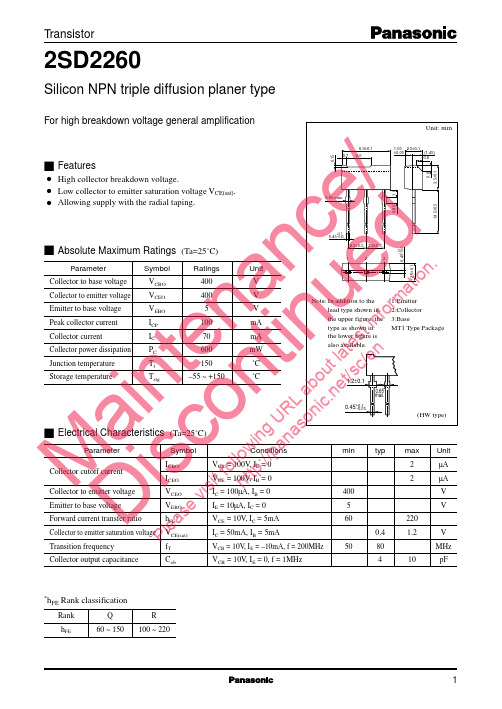
12Request for your special attention and precautions in using the technical information andsemiconductors described in this book(1)If any of the products or technical information described in this book is to be exported or provided to non-residents, the laws andregulations of the exporting country, especially, those with regard to security export control, must be observed. (2)The technical information described in this book is intended only to show the main characteristics and application circuit examplesof the products, and no license is granted under any intellectual property right or other right owned by our company or any other company. Therefore, no responsibility is assumed by our company as to the infringement upon any such right owned by any other company which may arise as a result of the use of technical information described in this book.(3)The products described in this book are intended to be used for standard applications or general electronic equipment (such as officeequipment, communications equipment, measuring instruments and household appliances). Consult our sales staff in advance for information on the following applications:– Special applications (such as for airplanes, aerospace, automobiles, traffic control equipment, combustion equipment, life support systems and safety devices) in which exceptional quality and reliability are required, or if the failure or malfunction of the prod-ucts may directly jeopardize life or harm the human body.– Any applications other than the standard applications intended.(4)The products and product specifications described in this book are subject to change without notice for modification and/or im-provement. At the final stage of your design, purchasing, or use of the products, therefore, ask for the most up-to-date Product Standards in advance to make sure that the latest specifications satisfy your requirements. (5)When designing your equipment, comply with the range of absolute maximum rating and the guaranteed operating conditions(operating power supply voltage and operating environment etc.). Especially, please be careful not to exceed the range of absolute maximum rating on the transient state, such as power-on, power-off and mode-switching. Otherwise, we will not be liable for any defect which may arise later in your equipment.Even when the products are used within the guaranteed values, take into the consideration of incidence of break down and failure mode, possible to occur to semiconductor products. Measures on the systems such as redundant design, arresting the spread of fire or preventing glitch are recommended in order to prevent physical injury, fire, social damages, for example, by using the products.(6)Comply with the instructions for use in order to prevent breakdown and characteristics change due to external factors (ESD, EOS,thermal stress and mechanical stress) at the time of handling, mounting or at customer's process. When using products for which damp-proof packing is required, satisfy the conditions, such as shelf life and the elapsed time since first opening the packages.(7)This book may be not reprinted or reproduced whether wholly or partially, without the prior written permission of MatsushitaElectric Industrial Co., Ltd.M a i n t e n a n D i s c o n t i n u eP le a s ev i s it f o l l o w i n g U R L a b o u t l a t e s t i n fo r mh t t p ://p a n a s o n i c .n e t /s c /e n。
PF525变频器技术手册

技术数据PowerFlex 525 交流变频器技术参数中文版说明书主题页码产品概述2产品目录号说明8技术参数9环境参数11认证12尺寸和重量13设计考虑因素15熔断器和断路器额定值25附件及尺寸29安全断开扭矩功能38其他资源422罗克韦尔自动化出版物 520-TD001A-ZH-E - 2013年2 月PowerFlex 525 交流变频器技术参数产品概述PowerFlex® 525 交流变频器采用创新型设计,功能全面多样,既可配合独立机器使用,也可简单方便地集成到系统中。
PowerFlex 525 可为 30 HP 至 22 kW 的应用项目提供常规用途控制。
PowerFlex 525 变频器集各类电机控制选项、通信功能、节能特性和标准安全功能于一身,且经济实用,适合种类广泛的应用项目。
利用 PowerFlex 525 变频器提供的下列关键特性,将最大程度提高您的系统性能和生产率。
PowerFlex 525 变频器特性模块化设计•整个功率范围全部采用标准控制模块。
•可拆卸式控制模块和电源模块可令您边配置边安装。
•MainsFree™ 配置允许使用标准 USB 电缆,简化了控制模块与 PC 之间的连接,可快速上传、下载和更新变频器的新设置。
•可同时支持两个附件卡,而不增加占用空间。
封装和安装•对于 A 、B 和 C 型框架变频器,可利用 DIN 导轨安装特性快捷方便地完成安装。
同时支持面板安装方式,以增加安装灵活性。
•当环境温度在 45 °C 以下时,可通过零间距叠加™ 方式节省宝贵的面板空间。
•所有 200 V 和 400 V 级别变频器均采用集成滤波器,提供了一种经济型方案,并符合 EN61800-3 C2 和 C3 类电磁兼容性要求。
而外部滤波器则确保所有级别的 PowerFlex 525 变频器符合 EN61800-3 C1、C2 和 C3 类电磁兼容性要求。
•可选的 IP 30,NEMA/UL 类型 1 导轨槽可方便地适应标准 IP 20 (NEMA 开放型) 产品,提供更高的环境等级。
KA5Q1265RFYDTU中文资料

Rev.1.0.4Features•Quasi Resonant Converter Controller•Internal Burst Mode Controller for Stand-by Mode •Pulse by Pulse Current Limiting •Over Current Latch Protection•Over V oltage Protection (Vsync: Min. 11V)•Internal Thermal Shutdown Function •Under V oltage Lockout•Internal High V oltage Sense FET •Auto-Restart ModeDescriptionThe Fairchild Power Switch(FPS) product family is specially designed for an off-line SMPS with minimal externalcomponents. The Fairchild Power Switch(FPS) consist of high voltage power SenseFET and current mode PWM controller IC.PWM controller features integrated fixed oscillator, undervoltage lock out, leading edge blanking, optimized gate turn-on/turn-off driver, thermal shut down protection, over voltage protection, temperature compensated precision current sources for loop compensation and fault protection circuit. compared to discrete MOSFET and controller or R CC switching converter solution, a Fairchild Power Switch(FPS) can reduce totalcomponent count, design size, and weight and at the same time increase & efficiency, productivity, and system reliability. It has a basic platform well suited for cost-effective design in quasi resonant converter as C-TV power supply.TO-220F-5L1. Drain2. GND3. V CC4. FB5. SyncTO-3PF-5L11KA5Q-SERIESKA5Q0765RT/KA5Q12656RT/KA5Q1265RF/KA5Q1565RFFairchild Power Switch(FPS)KA5Q-SERIESAbsolute Maximum Ratings(Ta=25°C, unless otherwise specified)Characteristic Symbol Value Unit KA5Q0765RTDrain-source Voltage V DSS650V Drain-Gate Voltage(R GS=1MΩ)V DGR650V Gate-Source(GND) Voltage V GS±30V Drain Current Pulsed(1)I DM15ADC Continuous Drain Current (Tc = 25°C)I D 3.8ADC Continuous Drain Current (Tc = 100°C)I D 2.4ADC Single Pulsed Avalanch Current(3)(Energy (2))I AS(E AS)20(570)A(mJ) Maximum Supply Voltage V CC,MAX40VInput Voltage RangeV FB-0.3 to V CC V V Sync-0.3 to 13VTotal Power Dissipation P D47W Operating Junction Temperature.T J+160°C Operating Ambient Temperature.T A-25 to +85°C Storage Temperature Range.T STG-55 to +150°C Thermal Resistance Rthjc 2.7°C/W ESD Capability, HBM Model (All pins) 2.0kV ESD Capability, Machine Model (All pins)300VKA5Q12656RTDrain-source Voltage V DSS650V Drain-Gate Voltage(R GS=1MΩ)V DGR650V Gate-Source(GND) Voltage V GS±30V Drain Current Pulsed(1)I DM21ADC Continuous Drain Current (Tc = 25°C)I D 5.3ADC Continuous Drain Current (Tc = 100°C)I D 3.4ADC Single Pulsed Avalanch Current(Energy (2))I AS(E AS)30(950)A(mJ) Maximum Supply Voltage V CC,MAX40VInput Voltage RangeV FB-0.3 to V CC V V Sync-0.3 to13VTotal Power Dissipation P D55W Operating Junction Temperature.T J+160°C Operating Ambient Temperature.T A-25 to +85°C Storage Temperature Range.T STG-55 to +150°C Thermal Resistance Rthjc 2.7°C/W ESD Capability, HBM Model (All pins) 2.0kV ESD Capability, Machine Model (All pins)300VKA5Q-SERIESAbsolute Maximum Ratings (Continued)(Ta=25°C, unless otherwise specified)Note:1. Repetitive rating : Pulse width limited by maximum junction temperature2. L = 10mH, V DD =50V, R G = 27Ω, starting Tj = 25°C3. L = 13uH, starting Tj = 25°CCharacteristic Symbol Value Unit KA5Q1265RF Drain-source VoltageV DSS 650V Drain-Gate Voltage(R GS =1M Ω)V DGR 650V Gate-Source(GND) Voltage V GS ±30V Drain Current Pulsed (1)I DM 36ADC Continuous Drain Current (Tc = 25°C)I D 8.3ADC Continuous Drain Current (Tc = 100°C)I D 5.3ADC Single Pulsed Avalanch Current(Energy (2))I AS (E AS )33(950)A(mJ)Maximum Supply Voltage V CC,MAX 40V Input Voltage Range V FB -0.3 to V CC V V Sync -0.3 to 13V Total Power DissipationP D 95W Operating Junction Temperature.T J +160°C Operating Ambient Temperature.T A -25 to +85°C Storage Temperature Range.T STG -55 to +150°C Thermal ResistanceRthjc2.7°C/W ESD Capability, HBM Model (All pins) 2.0kV ESD Capability, Machine Model (All pins)300VKA5Q1565RF Drain-source VoltageV DSS 650V Drain-Gate Voltage(R GS =1M Ω)V DGR 650V Gate-Source(GND) Voltage V GS ±30V Drain Current Pulsed (1)I DM 60ADC Continuous Drain Current (Tc = 25°C)I D 10.3ADC Continuous Drain Current (Tc = 100°C)I D 6.6ADC Single Pulsed Avalanch Current(Energy (2))I AS (E AS )36(1050)A(mJ)Maximum Supply Voltage V CC,MAX 40V Input Voltage Range V FB -0.3 to V CC V V Sync -0.3 to 13V Total Power DissipationP D 98W Operating Junction Temperature.T J +160°C Operating Ambient Temperature.T A -25 to +85°C Storage Temperature Range.T STG -55 to +150°C Thermal ResistanceRthjc2.7°C/W ESD Capability, HBM Model (All pins) 2.0kV ESD Capability, Machine Model (All pins)300VKA5Q-SERIESElectrical Characteristics (SFET part)(Ta=25°C unless otherwise specified)Parameter Symbol Conditions Min.Typ.Max.Unit KA5Q0765RTDrain-Source Breakdown Voltage BV DSS V GS=0V, I D=50µA650--VZero Gate Voltage Drain Current I DSS V DS=Max., Rating, V GS=0V--200µA V DS=0.8Max., Rating,V GS=0V, T C=85°C--300µAStatic Drain-Source on Resistance(1)R DS(on)V GS=10V, I D=4.0A- 1.3 1.6ΩInput Capacitance CissV GS=0V, V DS=25V,f = 1MHz -1110-pFOutput Capacitance Coss-105-Reverse Transfer Capacitance Crss-50-Turn on Delay Time td(on)V DD=0.5BV DSS, I D=7.0A(MOSFET switchingtime are essentiallyindependent ofoperating temperature)-25-nSRise Time tr-55-Turn Off Delay Time td(off)-80-Fall Time tf-50-Total Gate Charge (Gate-Source+Gate-Drain)QgV GS=10V, I D=7.0A,V DS=0.5BV DSS(MOSFETSwitching time areEssentially independent ofOperating temperature)-5774nCGate-Source Charge Qgs-9.3-Gate-Drain (Miller) Charge Qgd-29.3-KA5Q12656RT/KA5Q1265RFDrain-Source Breakdown Voltage BV DSS V GS=0V, I D=50µA650--VZero Gate Voltage Drain Current I DSS V DS=Max., Rating, V GS=0V--200µA V DS=0.8Max., Rating,V GS=0V, T C=85°C--300µAStatic Drain-Source on Resistance (1)R DS(on)V GS=10V, I D=6A-0.70.9ΩInput Capacitance CissV GS=0V, V DS=25V,f = 1MHz -1820-pFOutput Capacitance Coss-185-Reverse Transfer Capacitance Crss-32-Turn on Delay Time td(on)V DD=0.5BV DSS, I D=12.0A(MOSFET switchingtime are essentiallyindependent ofoperating temperature)-38-nSRise Time tr-120-Turn Off Delay Time td(off)-200-Fall Time tf-100-Total Gate Charge (Gate-Source+Gate-Drain)QgV GS=10V, I D=12.0A,V DS=0.5BV DSS(MOSFETSwitching time areEssentially independent ofOperating temperature)-6078nCGate-Source Charge Qgs-10-Gate-Drain (Miller) Charge Qgd-30-KA5Q-SERIESAbsolute Maximum Ratings (SFET Part)(Ta=25°C, unless otherwise specified)Note:1. Pulse test: Pulse width ≤ 300µS, duty cycle ≤ 2%Characteristic Symbol Test condition Min.Typ.Max.Unit KA5Q1565RFDrain-Source Breakdown Voltage BV DSS V GS =0V, I D =50µA 650--V Zero Gate Voltage Drain Current I DSS V DS =Max., Rating, V GS =0V--200µA V DS =0.8Max., Rating,V GS =0V, T C =85°C --300µA Static Drain-Source on Resistance (Note)R DS(ON)V GS =10V, I D =7.3A -0.50.65W Input Capacitance Ciss V GS =0V, V DS =25V,f=1MHz-2580-pFOutput CapacitanceCoss -270-Reverse Transfer Capacitance Crss -50-Turn on Delay Time td(on)V DD =0.5BV DSS , I D =14.6A (MOSFET switching time are essentially independent ofoperating temperature)-50-nSRise Timetr -155-Turn Off Delay Time td(off)-270-Fall Timetf -125-Total Gate Charge(Gate-Source+Gate-Drain)Qg V GS =10V, I D =14.6A,V DS =0.8BV DSS (MOSFET switching time areessentially independent of operating temperature)-90117nCGate-Source Charge Qgs -15-Gate-Drain (Miller) ChargeQgd-45-KA5Q-SERIESElectrical Characteristics (Control Part)(Ta=25°C unless otherwise specified)Parameter Symbol Conditions Min.Typ.Max.Unit UVLO SECTIONStart Threshold Voltage V START V FB=GND141516V Stop Threshold Voltage V STOP V FB=GND8910V OSCILLATOR SECTIONInitial Frequency F OSC-182022kHz Voltage Stability F STABLE12V ≤ V CC ≤ 23V013% Temperature Stability (Note2)∆F OSC-25°C ≤ Τa≤ 85°C0±5±10% Maximum Duty Cycle D MAX-929598% Minimum Duty Cycle D MIN---0% FEEDBACK SECTIONFeedback Source Current I FB V FB=GND0.70.9 1.1mA Shutdown Feedback Voltage V SD V FB ≥ 6.9V 6.97.58.1V Shutdown Delay Current I DELAY V FB=5V456µA SYNC. SECTIONNormal Sync High Threshold Voltage V NSH V CC=16V, Vfb=5V 4.0 4.6 5.2V Normal Sync Low Threshold Voltage V NSL V CC=16V, Vfb=5V 2.3 2.6 2.9V Burst Sync High Threshold Voltage V BSH V CC=10.5V, Vfb=0V 3.2 3.6 4.0V Burst Sync Low Threshold Voltage V BSL V CC=10.5V, Vfb=0V 1.1 1.3 1.5V BURST MODE SECTIONBurst Mode Low Threshold Voltage V BURL V FB=0V10.411.011.6V Burst Mode High Threshold Voltage V BURH V FB=0V11.412.012.6V Burst Mode Enable Feedback Voltage V BEN V CC=10.5V0.7 1.0 1.3V Burst Mode Peak Current Limit(Note4)I BURPK V CC=10.5V , V FB=0V0.650.85 1.1A CURRENT LIMIT(SELF-PROTECTION)SECTIONPeak Current Limit (Note4)I OVER KA5Q0765RT 4.40 5.00 5.60A KA5Q12656RT 5.28 6.00 6.72KA5Q1265RF7.048.008.96KA5Q1565RF10.1211.5012.88PROTECTION SECTIONOver Voltage Protection V OVP V SYNC ≥ 11V111213V Over Current Latch voltage(Note3)V OCL-0.9 1.0 1.1V Thermal Shutdown Tempature(Note2)TSD-140160-°CKA5Q-SERIESElectrical Characteristics (Control Part) (Continued)(Ta=25°C unless otherwise specified)Note:1. These parameters is the Current Flowing in the Control IC.2. These parameters, although guaranteed, are not 100% tested in production3. These parameters, although guaranteed, are tested in EDS(wafer test) process4. These parameters are indicated Inductor Current.ParameterSymbolConditionsMin.Typ.Max.UnitTOTAL DEVICE SECTION Start Up CurrentI START V FB =GND, V CC =14V -0.10.2mAOperating Supply Current(Note1)I OP V FB =GND, V CC =16V -1018mAI OP(MIN)V FB =GND, V CC =12V I OP(MAX)V FB =GND, V CC =28V PRIMARY SIDE REGULATION SECTION (ONLY KA5Q0765RT/KA5Q12656RT)Primary Regulation Threshold Voltage V PR I FB =700uA, V FB =4V32.032.533.0V Primary Regulation TransconductanceG PR- 2.02.6-mA/VTypical Performance CharacteristicsFigure 1. Start Threshold VoltageFigure 2. Stop Threshold VoltageFigure 3. Start Up CurrentFigure 4. Operting Supply CurrentFigure 6. Maximum DutyTypical Performance Characteristics (Continued)Figure 7. Feedback Offset VoltageFigure 8. Feedback Source CurrentFigure 9. Over Voltage ProtectionFigure 10. Shutdown Feedback VoltageFigure 12. Burst mode Enable Feedback VoltageKA5Q-SERIES Typical Performance Characteristics (Continued)Figure 13. Burst mode Low Threshold Voltage Figure 14. Burst mode HighThreshold VoltageFigure 15. Burst Sync. High Threshold Voltage Figure 16. Burst Sync. Low Threshold VoltageFigure17. Primary Regulation Threshold Voltage Figure 18. Primary Regulation TransconductanceTypical Performance Characteristics (Continued)Figure 19. Peak Current Limit Figure 20. Burst mode Peak Current LimitFigure 21. Normal Sync. High Threshold Voltage Figure 22. Normal Sync. Low Threshold Voltage11Package DimensionsTO-220F-5L12Package Dimensions (Continued)13Package Dimensions (Continued)14Package Dimensions (Continued)1512/16/04 0.0m 001Stock#DSxxxxxxxx2004 Fairchild Semiconductor CorporationLIFE SUPPORT POLICYFAIRCHILD’S PRODUCTS ARE NOT AUTHORIZED FOR USE AS CRITICAL COMPONENTS IN LIFE SUPPORT DEVICES OR SYSTEMS WITHOUT THE EXPRESS WRITTEN APPROVAL OF THE PRESIDENT OF FAIRCHILD SEMICONDUCTOR CORPORATION. As used herein:1.Life support devices or systems are devices or systemswhich, (a) are intended for surgical implant into the body, or (b) support or sustain life, and (c) whose failure to perform when properly used in accordance with instructions for use provided in the labeling, can bereasonably expected to result in a significant injury of the user.2. A critical component in any component of a life supportdevice or system whose failure to perform can bereasonably expected to cause the failure of the life support device or system, or to affect its safety or effectiveness.DISCLAIMERFAIRCHILD SEMICONDUCTOR RESERVES THE RIGHT TO MAKE CHANGES WITHOUT FURTHER NOTICE TO ANY PRODUCTS HEREIN TO IMPROVE RELIABILITY, FUNCTION OR DESIGN. FAIRCHILD DOES NOT ASSUME ANYLIABILITY ARISING OUT OF THE APPLICATION OR USE OF ANY PRODUCT OR CIRCUIT DESCRIBED HEREIN; NEITHER DOES IT CONVEY ANY LICENSE UNDER ITS PATENT RIGHTS, NOR THE RIGHTS OF OTHERS.Ordering InformationTU : Non Forming Type YDTU : Forming TypeProduct Number Package Rating I OVER KA5Q0765RTTU TO-220F-5L 650V, 7A 5A KA5Q0765RTYDTU TO-220F-5L (Forming)KA5Q12656RTTU TO-220F-5L 650V,12A 6A KA5Q12656RTYDTU TO-220F-5L (Forming)KA5Q1265RFTU TO-3PF-5L 650V,12A 8A KA5Q1265RFYDTU TO-3PF-5L (Forming)KA5Q1565RFTU TO-3PF-5L 650V,15A11.5AKA5Q1565RFYDTUTO-3PF-5L (Forming)。
C2260资料

Pin Connections
1 2 3 4 Voltage Control (Vc) Ground (Case) RF output Supply Voltage Input (Vs)
Marking
C2260-xxxx frequency * C AYYWW
Vectron International ·
Max. 16.5 0.3 5 60
Units pF VDC VDC ns %
Condition
Ordering Code5 RFH
with Vs=3.3V and 15pF load with Vs=3.3V and 15pF load @ (Voh-Vol)/2
50
Frequency Tuning (EFC)
v.2005-12-15 · page 1 of 5 Vectron Asia Pacific Sales Office 1F-2F, No 8 Workshop, No 308 Fenju Road, WaiGaoQiao Free Trade Zone, Pudong, Shanghai, P.R. China 200131 +86 21 5048 0777 tel. +86 21 5048 1881 fax
RF output
Parameter Signal [Standard] Load R || C Output power Min 9 9 0.7 Typ Max. clipped Sinewave 10 11 10 11 Units kΩ pF Vpp Condition > 12.288MHz Ordering Code5 RFC
Weight Processing & Packing
安捷伦仪器使用说明书中文

Alpha安捷伦B1500A半导体器件分析仪用户!ˉ的GUID安捷伦科技公司声明?安捷伦科技公司2005年,2006年,2007年,2008本手册的任何部分不得转载任何形式或通过任何手段(包括电子电子存储和检索或翻译成外国语言)事先同意MENT和安捷伦的书面同意作为由美国科技公司在美国和国际版权法。
手册部件号B1500-90000版2005年7月第1版,第2版,2005年12月2006年4月第3版第4版,2007年1月2007年6月5日,版第6版,2007年11月2008年10月7日,版安捷伦科技公司5301史蒂文斯溪大道95051美国加利福尼亚州圣克拉拉保证本文档中所含的物质是提供MENT!°为是,±,是苏如有更改,恕不另行通知,在以后的版本。
此外,最大而且,在适用法律法律,安捷伦提供任何保证,明示或暗示,关于本手册的任何信息所载,包括但不不限于隐含保证为杆的适销性和适用性特定用途。
安捷伦不得承担错误或偶然或在相应的损害赔偿连接TION的家具,使用,或每本文件或任何性能所载资料。
应该安捷伦与用户有一个单独的与保修的书面协议在这个物质的范围,涵盖记录与这些冲突条款,在保修则以协议arate中的协议为准。
技术许可硬件和/或软件描述这份文件是依照许可可用于复制或只在雅跳舞的许可条款。
有限权利如果软件在使用的一种表现美国政府的首要合同或道,软件交付和许可!°商业计算机软件!±ADFAR252.227-7014(1995年6月)的定义,或作为一个!°商业项目!FA±定义2.101(a)或°有限计算机软!洁具!±作为定义在FAR52.227-19(六月1987)或任何相当机构法规或合同条款。
使用,重复或disclo的软件肯定是受安捷伦科技nologies!ˉ标准商业许可条款和非DOD部门和美国政府机构没有获得更大而不是限制权利定义在FAR 52.227-19中(C)(1-2)(6月1987年)。
pt2262中文资料_数据手册_参数

pins are used as data pins, they can be set only to “0” or “1”.
Transmission Enable.
/TE
I Active Low Signal. PT2262 outputs the encoded waveform to DOUT
Data Output Pin.
DOUT
O The encoded waveform is serially outputted to this pin. When PT2262
is not transmitting, DOUT outputs low (Vss) voltage.
Vcc
- Positive Power Supply
when this pin is pulled to low.
OSC1 OSC2
O Oscillator Pin No.1 I Oscillator Pin No.2
A resistor connected between these two pins determine the fundamental frequency of the PT2262.
DESCRIPTION
PT2262 is a remote control encoder paired with PT2272 utilizing CMOS Technology. It encodes data and address pins into a serial coded waveform suitable for RF or IR modulation. PT2262 has a maximum of 12 bits of tri-state address pins providing up to 531,441 (or 312) address codes; thereby, drastically reducing any code collision and unauthorized code scanning possibilities.
AM26LS31PC中文资料

Symbol VIL VIH IIL IIH
Min – 2.0 –
– – VIK VOL VOH IOS IO(Z) – – IO(off) – – VOS – VOS VOD ∆VOD ICCX – 2.0 – – – – 2.5 – 30
2
MOTOROLA ANALOG IC DEVICE DATA
元器件交易网
AM26LS31
Figure 1. Three–State Enable Test Circuit and Waveforms
To Scope (Input) 3.0 V or Gnd Input Inv Output To Scope Output
Characteristic Propagation Delay Times High to Low Output Low to High Output Output Skew Propagation Delay – Control to Output (CL = 10 pF, RL = 75 Ω to Gnd) (CL = 10 pF, RL = 180 Ω to VCC) (CL = 30 pF, RL = 75 Ω to Gnd) (CL = 30 pF, RL = 180 Ω to VCC) tPHZ(E) tPLZ(E) tPZH(E) tPZL(E) Symbol tPHL tPLH Min – – – – – – – Typ – – – – – – – Max 20 20 6.0 30 35 40 45 ns ns Unit ns
元器件交易网
Order this document by AM26LS31/D
- 1、下载文档前请自行甄别文档内容的完整性,平台不提供额外的编辑、内容补充、找答案等附加服务。
- 2、"仅部分预览"的文档,不可在线预览部分如存在完整性等问题,可反馈申请退款(可完整预览的文档不适用该条件!)。
- 3、如文档侵犯您的权益,请联系客服反馈,我们会尽快为您处理(人工客服工作时间:9:00-18:30)。
FeaturesBLOCK DIAGRAMs Full militarized QED RM5260 microprocessorsDual Issue superscalar QED RISCMark ™ - can issue one integer and one floating-point instruction per cycle microprocessor - can issue one integer and one floating-point instruction per cycleq 100, 133 and 150MHz frequency (200MHz future option) Consult Factory for latest speeds q 260 Dhrystone2.1 MIPSq SPECInt95 4.8. SPECfp95 5.1sHigh performance system interface compatible with R4600, R4700 and R5000q 64-bit multiplexed system address/data bus for optimum price/performance up to 100 MHz operating frequency q High performance write protocols maximize uncached write bandwidthq Operates at input system clock multipliers of 2 through 8q 5V tolerant I/O'sq IEEE 1149.1 JTAG boundary scansIntegrated on-chip caches - up to 3.2GBps internal data rate q 16KB instruction - 2 way set associative q 16KB data - 2 way set associative q Virtually indexed, physically taggedq Write-back and write-through on per page basisq Pipeline restart on first double for data cache misses sIntegrated memory management unitq Fully associative joint TLB (shared by I and D translations)q 48 dual entries map 96 pagesq Variable page size (4KB to 16MB in 4x increments)sEmbedded supply de-coupling capacitors and Pll filter componentssHigh-performance floating point unit - up to 400 MFLOPS q Single cycle repeat rate for common single precision operations and some double precision operationsq Two cycle repeat rate for double precision multiply and double precision combined multiply-add operations q Single cycle repeat rate for single precision combined multiply-add operation sMIPS IV instruction setq Floating point multiply-add instruction increases performance in signal processing and graphics applicationsq Conditional moves to reduce branch frequency q Index address modes (register + register)sEmbedded application enhancementsq Specialized DSP integer Multiply-Accumulate instruction and 3 operand multiply instruction q I and D cache locking by setq Optional dedicated exception vector for interrupts sFully static CMOS design with power down logicq Standby reduced power mode with WAIT instruction q 5 Watts typical at 3.3V , less than 175 mwatts in Standby s 208-lead CQFP , cavity-up package (F17)s208-lead CQFP , inverted footprint (F24), Intended to duplicate the commercial QED footprin t (Consult Factory)s179-pin PGA package (Future Product ) (P10)Store BufferData Set A Data Tag A DTLB Physical Data Tag BInstruction Set AInteger Instruction RegisterFP Instruction RegisterInstruction Set B Address Buffer Instruction Tag A ITLB PhysicalInstruction Tag BSys ADWrite Buffer Read Buffer Data Set BDBusControlFloating-point Register File Joint TLBTagAux TagIntIBusFloating-point Coprocessor 0Unpacker/PackerMAdd, Add, Sub,CvtPC Incrementer Branch Adder DVALoad AlignerInteger Register File Integer/Address Adder Data TLB Virtual Shifter/Store AlignerLogic Unit Integer Multiply, DivideInteger ControlInstruction TLB Virtual F l o a t i n g p o i n t C o n t r o lPhase Lock LoopInstruction SelectFPIBusABusSystem/MemoryControlProgram CounterIVADiv, SqRt64-Bit Superscaler MicroprocessorACT5260DESCRIPTION:The ACT5260 is a highly integrated superscalar microprocessor that implements a superset of the MIPS IV Instruction Set Architecture(ISA). It has a high performance 64-bit integer unit, a high throughput, fully pipelined 64-bit floating point unit, an operating system friendly memory management unit with a 48-entry fully associative TLB, a 16 KByte 2-way set associative instruction cache, a 16 KByte 2-way set associative data cache, and a high-performance 64-bit system interface. The ACT5260 can issue both an integer and a floating point instruction in the same cycle.The ACT5260 is ideally suited for high-end embedded control applications such as internetworking, high performance image manipulation, high speed printing, and 3-D visualization.HARDWARE OVERVIEWThe ACT5260 offers a high-level of integration targeted at high-performance embedded applications. Some of the key elements of the ACT5260 are briefly described below. Superscalar DispatchThe ACT5260 has an efficient asymmetric superscalar dispatch unit which allows it to issue an integer instruction and a floating-point computation instruction simultaneously. With respect to superscalar issue, integer instructions include alu, branch, load/store, and floating-point load/store, while floating-point computation instructions include floating-point add, subtract, combined multiply-add, converts, etc. In combination with its high throughput fully pipelined floating-point execution unit, the superscalar capability of the ACT5260 provides unparalleled price/performance in computationally intensive embedded applications.CPU RegistersLike all MIPS ISA processors, the ACT5260 CPU has a simple, clean user visible state consisting of 32 general purpose registers, two special purpose registers for integer multiplication and division, a program counter, and no condition code bits. PipelineFor integer operations, loads, stores, and other non-floating-point operations, the ACT5260 uses the simple 5-stage pipeline also found in the circuits R4600, R4700, and R5000. In addition to this standard pipeline, the ACT5260 uses an extended seven stage pipeline for floating-point operations. Like the R5000, the ACT5260 does virtual to physical translation in parallel with cache access.Integer UnitLike the R5000, the ACT5260 implements the MIPS IV Instruction Set Architecture, and is therefore fully upward compatible with applications that run on processors implementing the earlier generation MIPS I-III instruction sets. Additionally, the ACT5260 includes two implementation specific instructions not found in the baseline MIPS IV ISA but that are useful in the embedded market place. Described in detail in the QED RM5260 datasheet, these instructions are integer multiply-accumulate and 3-operand integer multiply.The ACT5260 integer unit includes thirty-two general purpose 64-bit registers, a load/store architecture with single cycle ALU operations (add, sub, logical, shift) and an autonomous multiply/divide unit. Additional register resources include: the HI/LO result registers for the two-operand integer multiply/ divide operations, and the program counter(PC). Register FileThe ACT5260 has thirty-two general purpose registers with register location 0 hard wired to zero. These registers are used for scalar integer operations and address calculation. The register file has two read ports and one write port and is fully bypassed to minimize operation latency in the pipeline.ALUThe ACT5260 ALU consists of the integer adder/ subtractor, the logic unit, and the shifter. The adder performs address calculations in addition to arithmetic operations, the logic unit performs all logical and zero shift data moves, and the shifter performs shifts and store alignment operations. Each of these units is optimized to perform all operations in a single processor cycleFor additional Detail Information regarding the operation of the Quantum Effect Design (QED) RISCMark™ RM5260™, 64-Bit Superscalar Microprocessor see the latest QED datasheet (Revision 1.1 July 1998).Absolute Maximum Ratings1Symbol Rating Range Units V TERM T erminal Voltage with respect to GND-0.52 to 4.6V Tc Operating T emperature-55 to +125°C T BIAS Case T emperature under Bias-55 to +125°C T STG Storage T emperature-55 to +125°CI IN DC Input Current203mAI OUT DC Output Current50mA Notes:1. Stresses above those listed under "AbsoluteMaximums Rating" may cause permanent damage to the device. This is a stress rating only and functional operation of the device at these or any other conditions above those indicated in the operational sections of this specification is not implied. Exposure to absolute maximum rating conditions for extended periods may affect device reliability.2. V IN minimum = -2.0V for pulse width less than 15nS. V IN maximum should not exceed +5.5 Volts.3. When V IN < 0V or V IN > Vcc.4. No more than one output should be shorted at one time. Duration of the short should not exceed more than 30 second.Recommended Operating ConditionsSymbol Parameter Minimum Maximum Units V CC Power Supply Voltage+3.135+3.465V V IH Input High Voltage0.7V CC V CC+ 0.5V V IL Input Low Voltage-0.50.2V CC V T C Operating Temperature Case -55+125°C For 133MHz Parts only -40+125°CDC Characteristics(V CC = 3.3V ±5%; 133MHz parts: Tc =-40°C to +125°C, All other parts Tc =-55°C to +125°C)Parameter Sym Conditions 100 / 133 / 150MHzUnits Min MaxOutput Low Voltage V OL1I OL = 20 µA-0.1V Output High Voltage V OH1I OL = 20 µA Vcc - 0.1-V Output Low Voltage V OL2I OL = 4 mA-0.4V Output High Voltage V OH2I OL = 4 mA 2.4-V Input High Voltage V IH0.7V CC V CC+ 0.5V Input Low Voltage V IL-0.50.2V CC V Input Current I IN1V IN = 0V-20+20µA Input Current I IN2V IN = V CC-20+20µA Input Current I IN3V IN = 5.5V-250+250µA Input Capacitance C IN-10pF Output Capacitance C OUT-10pFAC Characteristics(V CC = 3.3V ±5%; 133MHz parts: Tc =-40°C to +125°C, All other parts Tc =-55°C to +125°C)Power ConsumptionParameter Symbol Conditions100MHz, 3.3V 133MHz, 3.3V 150MHz, 3.3V Units Typ 5Max Typ 5Max Typ 5Max Active Operating Supply CurrentI CC1C L = 0pF ,No SysAD activity8001550800155010001750mA I CC2C L = 50pF , R4000 writeprotocol without FPU operation 100017501000175011501950mA I CC3C L = 50pF , write re-issue or pipelined writes 110020001100200012502250mA Standby CurrentI SB1C L = 0pF 7515075150100175mA I SB1C L = 50pF7515075150100175mANotes:5. Typical integer instruction mix and cache miss rates.Capacitive Load DerationSymbol Parameter100 / 133 / 150MHz Units MinimumMaximumC LDLoad Derate-2ns/25pFClock ParametersParameter Symbol Test Conditions100/133/150MHz Units Min Max SysClock High t SCHigh T 4-ns SysClock Low t SCLowT 4-ns SysClock Frequency 63375MHz SysClock Period t SCP -30ns Clock Jitter for SysClock t JitterIn -±250ps SysClock Rise Time t SCRise -5ns SysClock Fall Time t SCFall -5ns ModeClock Period t ModeCKP -256*t SCP ns JTAG Clock Periodt JTAGCKP -4*t SCPnsNotes:6. Operation of the ACT5260 is only guaranteed with the Phase Loop enabled.System Interface Parameters7Parameter Symbol Test Conditions100MHz133MHz150MHzUnits Min Max Min Max Min MaxData Output8t DO mode14...13 = 10 (fastest) 1.07.0 1.07.0 1.07.0ns mode14...13 = 11 1.07.5 1.07.5 1.07.5ns mode14...13 = 00 1.08.0 1.08.0 1.08.0ns mode14...13 = 01 (slowest) 1.08.5 1.08.5 1.08.5nsData Setup t DS t RISE = 5ns 5.0- 5.0- 5.0-ns Data Hold t DH t FALL= 5ns 2.0- 2.0- 2.0-ns Notes: -7. Timmings are are measured from from 1.5V of the clock to 1.5V of the signal.8. Capacitive load for all output timing is 50pF.Boot Time Interface ParametersParameter Symbol Test Conditions 100/133/150MHzUnits Min MaxMode Data Setup t DS4-SysClock cycles Mode Data Hold t DH0-SysClock cycles1.8401.8801.700BSC 1.700BSC 1.8401.880V U T R P N M L K J H G F E D C B A123456789101112131415161718Bottom ViewSide ViewFuture Package – "P10" – PGA 179 Pins (Advanced)1.131 (28.727) SQ 1.109 (28.169) SQ1.009 (25.63).9998 (25.37)51 Spaces at .0197(51 Spaces at .50).0236 (.51).0158 (.49)52120815615710510453Pin 1 ChamferDetail "A"0°±5°1.331 (33.807)1.269 (32.233).005 (.127).008 (.258).055 (1.397)REF .055 (1.397).045 (1.143).115 (2.921)MAX.960 (24.384) SQREF.130 (3.302)MAX.010R MIN.010R MIN .009 (.253).007 (.178).015 (.381).009 (.229).100 (2.540).080 (2.032)Package Information – "F17" – CQFP 208 LeadsDetail "A"BSC.100.221MAX.018.050Note: Pin rotation is opposite of QEDs PQUAD due to cavity-up construction..035 (.889).025 (.635)Units: Inches (Millimeters)ACT5260 Microprocessor CQFP Pinouts – "F17"Pin #Function Pin #Function Pin # Function Pin # Function 1Vcc (3.3V)53NC105Vcc (3.3V)157NC2NC54NC106NMI*158NC3NC55NC107ExtRqst*159NC4Vcc (3.3V)56Vcc (3.3V)108Reset*160NC5Vss57Vss109ColdReset*161Vcc (3.3V) 6SysAD458ModeIn110VccOK162Vss7SysAD3659RdRdy*111BigEndian163SysAD28 8SysAD560WrRdy*112Vcc (3.3V)164SysAD60 9SysAD3761ValidIn*113Vss165SysAD29 10Vcc (3.3V)62ValidOut*114SysAD16166SysAD61 11Vss63Release*115SysAD48167Vcc (3.3V) 12SysAD664VccP116Vcc (3.3V)168Vss13SysAD3865VssP117Vss169SysAD30 14Vcc (3.3V)66SysClock118SysAD17170SysAD62 15Vss67Vcc (3.3V)119SysAD49171Vcc (3.3V) 16SysAD768Vss120SysAD18172Vss17SysAD3969Vcc (3.3V)121SysAD50173SysAD31 18SysAD870Vss122Vcc (3.3V)174SysAD63 19SysAD4071Vcc (3.3V)123Vss175SysADC2 20Vcc (3.3V)72Vss124SysAD19176SysADC6 21Vss73SysCmd0125SysAD51177Vcc (3.3V) 22SysAD974SysCmd1126Vcc (3.3V)178Vss23SysAD4175SysCmd2127Vss179SysADC3 24Vcc (3.3V)76SysCmd3128SysAD20180SysADC7 25Vss77Vcc (3.3V)129SysAD52181Vcc (3.3V) 26SysAD1078Vss130SysAD21182Vss27SysAD4279SysCmd4131SysAD53183SysADC0 28SysAD1180SysCmd5132Vcc (3.3V)184SysADC4 29SysAD4381Vcc (3.3V)133Vss185Vcc (3.3V) 30Vcc (3.3V)82Vss134SysAD22186Vss31Vss83SysCmd6135SysAD54187SysADC1 32SysAD1284SysCmd7136Vcc (3.3V)188SysADC5 33SysAD4485SysCmd8137Vss189SysAD0 34Vcc (3.3V)86SysCmdP138SysAD23190SysAD32 35Vss87Vcc (3.3V)139SysAD55191Vcc (3.3V) 36SysAD1388Vss140SysAD24192Vss37SysAD4589Vcc (3.3V)141SysAD56193SysAD1 38SysAD1490Vss142Vcc (3.3V)194SysAD33 39SysAD4691Vcc (3.3V)143Vss195Vcc (3.3V) 40Vcc (3.3V)92Vss144SysAD25196Vss41Vss93Int0*145SysAD57197SysAD2 42SysAD1594Int1*146Vcc (3.3V)198SysAD34 43SysAD4795Int2*147Vss199SysAD3 44Vcc (3.3V)96Int3*148SysAD26200SysAD35 45Vss97Int4*149SysAD58201Vcc (3.3V) 46ModeClock98Int5*150SysAD27202Vss47JTDO99Vcc (3.3V)151SysAD59203NC48JTDI100Vss152Vcc (3.3V)204NC49JTCK101NC153Vss205NC50JTMS102NC154NC206NC51Vcc (3.3V)103NC155NC207Vcc (3.3V) 52Vss104NC156Vss208VssOrdering InformationPart NumberScreeningSpeed (MHz)Package ACT-5260PC-100F17C Commercial Temperature (0°C to +70°C)100 208 Lead CQFP ACT-5260PC-133F17C Commercial Temperature (0°C to +70°C)133 208 Lead CQFP ACT-5260PC-150F17C Commercial Temperature (0°C to +70°C)150 208 Lead CQFP ACT-5260PC-100F17I Industrial Temperature (-40°C to +85°C)100 208 Lead CQFP ACT-5260PC-133F17I Industrial Temperature (-40°C to +85°C)133 208 Lead CQFP ACT-5260PC-150F17I Industrial Temperature (-40°C to +85°C)150 208 Lead CQFP ACT-5260PC-100F17T Military Temperature (-55°C to +125°C)100 208 Lead CQFP ACT-5260PC-133F17T Reduced Military Temperature (-40°C to +125°C)133 208 Lead CQFP ACT-5260PC-150F17T Military Temperature (-55°C to +125°C)150 208 Lead CQFP ACT-5260PC-100F17M Military Temperature, Screened* (-55°C to +125°C)100 208 Lead CQFP ACT-5260PC-133F17M Reduced Military Temperature, Screened* (-40°C to +125°C)133 208 Lead CQFP ACT-5260PC-150F17MMilitary Temperature, Screened* (-55°C to +125°C)150208 Lead CQFPAeroflex Circuit Technology 35 South Service RoadPlainview New York 11803 Telephone: (516) 694-6700FAX: (516) 694-6715Toll Free Inquiries: (800) /act1.htmE-Mail: sales-act@Specifications subject to change without notice.C I R C U I T T E C H N O L O G YPart Number BreakdownACT–5260PC –100F17MAeroflex Circuit TechnologyBase Processor Type 100 = 100MHz133 = 133MHz (Screening: T & M -40°C to +125°C only)150 = 150MHz200 = 200MHZ (Future option)Cache StylePackage Type & SizeC = Commercial Temp, 0°C to +70°C I = Industrial T emp, -40°C to +85°C T = Military Temp, -55°C to +125°CM = Military T emp, -55°C to +125°C, Screened *Q = MIL-PRF-38534 Compliant/SMD if applicableScreening* Screened to the individual test methods of MIL-STD-883PC = Primary Cache Maximum Pipeline Freq.Surface Mount PackageF17 = 1.120" SQ 208 Lead CQFPF24 = 1.120" SQ Inverted 208 Lead CQFP (Consult Factory)Thru-Hole PackageP10 = 1.86"SQ PGA 179 pins with shoulder Future Product。