PE4420中文资料
442SA2TADN中文资料
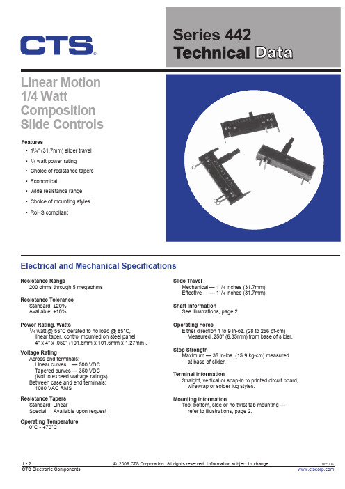
®Linear Motion 1/4 Watt Composition Slide Controls•11/4" (31.7mm) slider travel•1/4watt power rating •Choice of resistance tapers •Economical•Wide resistance range•Choice of mounting stylesElectrical and Mechanical SpecificationsResistance Range200 ohms through 5 megaohmsResistance ToleranceStandard:±20%Available:±10%Power Rating, Watts1/4watt @ 55°C derated to no load @ 85°C,linear taper, control mounted on steel panel4" x 4" x .050" (101.6mm x 101.6mm x 1.27mm). Voltage RatingAcross end terminals:Linear curves — 500 VDCTapered curves — 350 VDC(Not to exceed wattage ratings)Between case and end terminals:1080 VAC RMSResistance TapersStandard:LinearSpecial:Available upon request Slide TravelMechanical — 11/4inches (31.7mm)Effective — 11/4inches (31.7mm)Shaft InformationSee illustrations, page 2.Operating ForceEither direction 1 to 9 in-oz. (28 to 256 gf-cm)Measured .250" (6.35mm) from base of slider.Stop StrengthMaximum — 35 in-lbs. (15.9 kg-cm) measuredat base of slider.Terminal InformationStraight, vertical or snap-in to printed circuit board,wirewrap or solder lug styles.Mounting InformationTop, bottom, side or no twist tab mounting —refer to illustrations, page 2.FeaturesOperating Temperature0°C - +70°C•RoHS compliant1-2©2006CTS C orporati o n. A ll r i g hts r eserved. I nformati o n s ubject t o c hange.9/21/06 CTS Electronic Components Ordering Information CTS Series 442DIMENSION:mmINCHSUGGESTED PANEL PIERCING VIEWED FROM TOP SIDE FOR TWIST TABS AND ACTUATOR FROM TOP SIDE FOR TWIST TABS SUGGESTED PANEL PIERCING VIEWED2.03851.77SUGGESTED PANEL PIERCING VIEWED FROMCENTERLINE OF CONTROL FOR VERTICAL P.C. TERMINALS CONTROL SIDE FOR STRAIGHT P.C. & WIREWRAP TERMINALSSUGGESTED PANEL PIERCING VIEWED FROMALTERNATE TERMINAL STYLESNO MOUNT2-2©2006CTS C orporati o n. A ll r i g hts r eserved. I nformati o n s ubject t o c hange.9/21/06 CTS Electronic Components CONTROL SIDE FOR SNAP-IN P.C. TERMINALSSUGGESTED PANEL PIERCING VIEWED FROM。
TC4429COA;TC4420COA;TC4429CPA;TC4420CPA;TC4420EPA;中文规格书,Datasheet资料
VDD Output
DS21419C-page 2
/
2004 Microchip Technology Inc.
1.0 ELECTRICAL CHARACTERISTICS
Absolute Maximum Ratings†
Supply Voltage ..................................................... +20V Input Voltage .................................. – 5V to VDD + 0.3V Input Current (VIN > VDD)................................... 50 mA Power Dissipation (TA ≤ 70°C)
- 4.5V to 18V • High Capacitive Load Drive Capability: 10,000 pF • Short Delay Time: 55 ns (typ.) • CMOS/TTL Compatible Input • Low Supply Current With Logic ‘1’ Input:
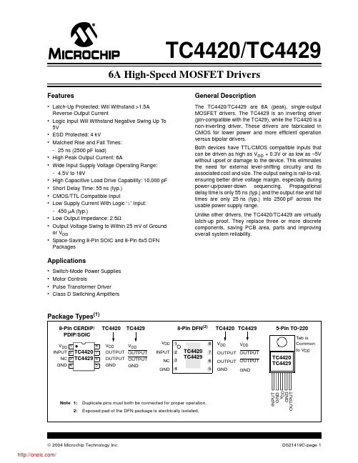
TC4420/TC4429
† Stresses above those listed under “Absolute Maximum Ratings” may cause permanent damage to the device. These are stress ratings only and functional operation of the device at these or any other conditions above those indicated in the operation sections of the specifications is not implied. Exposure to Absolute Maximum Rating conditions for extended periods may affect device reliability.
TLRO4420中文资料

12
6
www.vishay.de • FaxBack +1-408-970-5600 2 (9)
Document Number 83045 Rev. A1, 04-Feb-99
元器件交易网
TLR.442.
Vishay Telefunken
Green (TLRG4420 ) Parameter Luminous intensity Dominant wavelength Peak wavelength Angle of half intensity Forward current Breakdown voltage Junction capacitance Test Conditions VF = 12 V VF = 12 V VF = 12 V VF = 12 V VS = 12 V IR = 10 mA VR = 0, f = 1 MHz Type Symbol IV ld lp ϕ IF VBR Cj Min 1.6 562 Typ 4 565 ±30 10 70 50 Max 575 Unit mcd nm nm deg mA V pF
12
6
Soft orange (TLRO4420 ) Parameter Luminous intensity Dominant wavelength Peak wavelength Angle of half intensity Forward current Breakdown voltage Junction capacitance Test Conditions VF = 12 V VF = 12 V VF = 12 V VF = 12 V VS = 12 V IR = 10 mA VR = 0, f = 1 MHz Type Symbol IV ld lp ϕ IF VBR Cj Min 4 598 Typ 10 605 ±30 10 70 50 Max 611 Unit mcd nm nm deg mA V pF
440变频器使用大全
1 2 3 4 5 6 7 8 9 10 11 12 13 14 15 16 17 A B C D E F
MICROMASTER 440变频器 0.12kW - 250kW
系统参数 排障 MICROMASTER 440 的技术规格 可选件
使用大全 用户文件
电磁兼容性 MICROMASTER 440 变频器的参数表 功能框图 二进制互联连接(BiCo)功能 通讯 高级操作板( AOP ) 编码器 制动电阻
Email: techsupport@ad.siemens.de 星期一至星期五:上午 7: 00 至下午 5: 00 (当地时间) 西门子(中国)有限公司技术支持部 北京 电话: 传真: 010 – 64738566 010 – 64731096,647地址 用户可以在以下网址查到技术资料和一般信息: http:///products/sd。 联系地址: 如果您在阅读本手册时有什麽疑问或问题,请根据本手册封底的地址与西门子公司的办事处联 系。
本手册中对某些有效的功能可能未加说明。但是,在新的控制装置 中或进行服务时,并不因为西门子公司提供了这些功能而要承担任 未经书面许可,不得翻印、传播、或使用本手册及其相关内 何责任。 容。违者将对所造成的损害负法律责任。西门子公司保留一切 编审过程中,我们对本手册的内容与所述的硬件和软件的一致性进 权利,包括由专利许可、实用样机注册、或工程设计等所产生 行了审核。但是,仍然可能存在矛盾和谬误的地方,不可能保证它 的所有权利。 们完全一致。我们将定期检查本手册中涵盖的内容,并在以后修订 的版本中予以必要的修正。欢迎提出改进的建议。 © Siemens AG 2001。保留一切权利。 西门子公司的手册都是用无氯纸张印刷的,这种纸张的生产原料来 源于可持续生长的森林。打印和装订的过程中未使用化学溶剂。 MICROMASTER® 是西门子公司已注册的商标。 保留不予先通知而修改本手册的权利。
HSDL-4420中文资料

HHigh-Performance IR Emitterand IR PIN Photodiode inSubminiature SMT PackageTechnical DataFeatures• Subminiature Flat Top and Dome PackageSize – 2x2 mm• IR Emitter875 nm TS AlGaAsIntensity – 17 mW/srSpeed – 40 ns• Wide Range of Drive Currents500 µA to 500 mA• IR DetectorPIN PhotodiodeHigh SensitivitySpeed – 7.5 ns• Flexible Lead ConfigurationsSurface Mount orThrough Hole Applications• Short Distance IR Links • IrDA Compatible• Small Handheld Devices PagersIndustrial Handhelds• Diffuse LANs• Wireless Audio DescriptionFlat Top PackageThe HSDL-4400 Series of flat topIR emitters use an untinted,nondiffused, truncated lens toprovide a wide radiation patternthat is useful for short distancecommunication where alignmentof the emitter and detector is notcritical. The HSDL-5400 Series offlat top IR detectors uses thesame truncated lens design as theHSDL-4400 Series of IR emitterswith the added feature of a blacktint that acts as an optical filter toreduce the effects of ambientlight, such as sun, incandescentand fluorescent light frominterfering with the IR signal.Dome PackageThe HSDL-4420 Series of domeIR emitters uses an untinted,nondiffused lens to provide a 24degree viewing angle with highon-axis intensity. The HSDL-5420Series of IR detectors uses thesame lens design as the HSDL-4420 IR emitter and optical filterused in the HSDL-5400 IRdetector.Lead ConfigurationAll of these devices are made byencapsulating LED and PINphotodiode chips on axial leadframes to form molded epoxysubminiature packages. A varietyof lead configurations is availableand includes: surface mount gullwing, yoke lead, or Z-bend andthrough hole lead bends at 2.54mm (0.100 inch) center spacing.TechnologyThe subminiature solid stateemitters utilize a highly optimizedLED material, transparent sub-strate aluminum gallium arsenide,TS AlGaAs. This material has avery high radiant efficiency,capable of producing high lightoutput over a wide range of drivecurrents and temperature.HSDL-44XX IR EmitterSeriesHSDL-54XX IR DetectorSeries5964-9018E4-68Device Selection GuideIR EmittersPart Number Device Description[1]Device Outline Drawing HSDL-4400LED, Flat Top, 110 deg AHSDL-4420LED, Dome, 24 deg BIR DetectorsPart Number Device Description[1]Device Outline Drawing HSDL-5400PIN Photodiode, Flat Top, 110 deg CHSDL-5420PIN Photodiode, Dome, 28 deg DPackage Configuration OptionsNotes:1. IR Emitters have untinted, nondiffused lenses and IR Detectors have black tinted, nondiffused lenses.2. Emitters and detectors are supplied in 12 mm embossed tape on 178 mm (7 inch) diameter reels, with 1500 unitsper reel. Minimum order quantity and order increment are in quantity of reels only.3. Emitters and detectors are supplied in bulk form in bags of 50 units.4-694-701.912.16(0.085)Package Dimensions(A) Flat Top Emitters0.76(0.030)R.0.18(0.007)(B) Dome Emitters0.50 (0.020) REF.NOTES:1. ALL DIMENSIONS ARE IN MILLIMETRES (INCHES).2. PROTRUDING SUPPORT TAB IS CONNECTED TO ANODE LEAD.3. LEAD POLARITY FOR THESE TS AlGaAs SUBMINIATURE LAMPS IS OPPOSITE TO THE LEAD POLARITY OF SUBMINIATURE LAMPS USING OTHER LED TECHNOLOGIES. CATHODE STRIPE MARKING IS BLACK.4-710.76(0.030)R.0.18(0.007) 2.16(0.085)(D) Dome Detectors(C) Flat Top Detectors0.50 (0.020) REF.NOTES:1. ALL DIMENSIONS ARE IN MILLIMETERS (INCHES).2. PROTRUDING SUPPORT TAB IS CONNECTED TO CATHODE LEAD.3. CATHODE STRIPE MARKING IS SILVER.4-720.76 (0.030) MAX.(F) “Yoke” Lead, Options 0210.76 (0.030) MAX.Package DimensionsThe following notes affect the package outline drawings E through I.1. The pinout represents the HSDL-54XX IR detectorswhere the protruding support tab is closest to the anode lead. While the pinout is reversed for the HSDL-44XXIR emitters where the pro-truding support tab is closest to the cathode lead.2. The protruding support tab of the HSDL-54XX is connected to the cathode lead. While the protruding support tab of the HSDL-44XX is connected to the anode lead.ALL DIMENSIONS ARE IN MILLIMETRES (INCHES)(E) Gull Wing Lead, Option 0114-73(G) Z-Bend Lead, Options 0310.76 (0.030) MAX.(H) Thru Hole Lead Option 1L1(I) Thru Hole Lead Option 1S1Package Dimensions: Surface Mount Tape and Reel Options (J) 12 mm Tape and Reel, Gull Wing Lead, Option 011GULL WING LEAD SUBMINIATURE PACKAGE NOTES:1. EMPTY COMPONENT POCKETS SEALED WITH TOP COVER TAPE.2. 7 INCH REEL – 1500 PIECES PER REEL.3. MINIMUM LEADER LENGTH AT EITHER END OF THE TAPE IS 500 mm.4. THE MAXIMUM NUMBER OF CONSECUTIVE MISSING DEVICES IS TWO.5. IN ACCORDANCE WITH ANSI/EIA RS-481 SPECIFICATIONS, THECATHODE IS ORIENTED TOWARDS THE TAPE SPROCKETS HOLE.At the time of this publication XX/96, Light Emitting Diodes (LEDs) that are contained in this product are regulated for eye safety in Europe by the Commission for European Electrotechnical Standardization (CENELEC) EN60825-1. Please refer to Application Brief I-008 for more information.4-74(K) 12 mm Tape and Reel, “Yoke” Lead, Option 021“YOKE” LEADSUBMINIATURE PACKAGE4-75(L) 12 mm Tape and Reel, Z-Bend Lead, Option 031Z-BEND LEADSUBMINIATURE PACKAGE4-76(M) 12 mm Tape and Reel4-77HSDL-44XX Absolute Maximum RatingsParameter Symbol Min.Max.Unit Ref. Peak Forward Current (Duty Factor = 20%,I FPK500mA Fig. 7, 8 Pulse Width = 100 µs)DC Forward Current I FDC100mA Fig. 6 Power Dissipation P DISS180mWReverse Voltage (I R = 100 µA)V R5VTransient Forward Current(10 µs Pulse)I FTR 1.0A[1] Operating Temperature T O-4085°CStorage Temperature T S-55100°CJunction Temperature T J110°CLead Solder Temperature260/5 s°C[1.6 mm (0.063 in.) from body]Reflow Soldering TemperaturesConvection IR235/90 s°CVapor Phase215/180 s°CNotes:1. The transient peak current in the maximum nonrecurring peak current the device can withstand without damaging the LED die andthe wire bonds.HSDL-44XX Electrical Characteristics at T A = 25°CParameter Symbol Min.Typ.Max.Unit Condition Ref. Forward Voltage V F 1.30 1.50 1.70V I FDC = 50 mA Fig. 21.40 1.67 1.85I FDC = 100 mA2.15I FPK = 250 mAForward Voltage∆V F/∆T-2.1mV/°C I FDC = 50 mA Fig. 3 Temperature Coefficient-2.1I FDC = 100 mASeries Resistance R S 2.8ΩI FDC = 100 mADiode Capacitance C O40pF0 V, 1 MHzReverse Voltage V R520V I R = 100 µAThermal Resistance,Rθjp170°C/WJunction to Pin4-78HSDL-44XX Optical Characteristics at T A = 25°CParameter Symbol Min.Typ.Max.Unit Condition Ref. Radiant Optical PowerHSDL-4400P O16mW I FDC = 50 mA30I FDC = 100 mA HSDL-4420P O16mW I FDC = 50 mA30I FDC = 100 mARadiant On-Axis IntensityHSDL-4400I E138mW/sr I FDC = 50 mA Fig. 4, 56I FDC = 100 mA15I FPK = 250 mA HSDL-4420I E91730mW/sr I FDC = 50 mA Fig. 4, 532I FDC = 100 mA85I FPK = 250 mARadiant On-Axis Intensity∆I E/∆T-0.35%/°C I FDC = 50 mA Temperature Coefficient-0.35I FDC = 100 mAViewing AngleHSDL-44002θ1/2110deg I FDC = 50 mA Fig. 9 HSDL-44202θ1/224deg I FDC = 50 mA Fig. 10 Peak WavelengthλPK860875895nm I FDC = 50 mA Fig. 1 Peak Wavelength∆λ/∆T0.25nm/°C I FDC = 50 mA Temperature CoefficientSpectral Width at FWHM∆λ37nm I FDC = 50 mA Fig. 1 Optical Rise and Fall t r/t f40ns I FPK = 50 mATimes, 10%-90%Bandwidth f c9MHz I FDC = 50 mA Fig. 11± 10 mA4-79HSDL-54XX Absolute Maximum RatingsParameter Symbol Min.Max.Unit Power Dissipation P DISS150mW Reverse Voltage (I R = 100 µA)V R40V Operating Temperature T O-4085°C Storage Temperature T S-55100°C Junction Temperature T J110°C Lead Solder Temperature [1.6 mm (0.063 in.) from body]260/5 s°C Reflow Soldering TemperaturesConvection IR235/90 s°C Vapor Phase215/180 s°C= 25°CHSDL-54XX Electrical Characteristics at T4-80HSDL-54XX Optical Characteristics at T = 25°C4-814-82R E L A T I V E R A D I A N T I N T E N S I T Yλ – WAVELENGTH – nmI F P K – P E A K F O R W A R D C U R R E N T – m AV F – FORWARD VOLTAGE – VFigure 3. Forward Voltage vs Ambient Temperature.V F – FO R W A R D V O L T A G E – V2.01.0T A – AMBIENT TEMPERATURE – °C1.21.81.61.4Figure 1. Relative Radiant Intensity vs. Wavelength.Figure 2. Peak Forward Current vs.Forward Voltage.Figure 5. Normalized RadiantIntensity vs. Peak Forward Current (0 to 10 mA).N O R M A LI Z E D R A D I A N T I N T E N S I T Y5.000I FPK – PEAK FORWARD CURRENT – mA 4.000.502.501.001.502.003.003.504.50N O R M A L I Z E D R A D I A N T I NT E N S I T Y1.000.01I FPK – FORWARD CURRENT – mA0.10I F D C – M A X I M U M D C F O R W A R D C U R R E N T – mA1200T A – AMBIENT TEMPERATURE – °C60100804020Figure 4. Normalized RadiantIntensity vs. Peak Forward Current.Figure 6. Maximum DC Forward Current vs. Ambient Temperature.Derated Based on T JMAX = 110°C.I F P K – P E A K F O R W A R D C U R R E N T – m A0t PW – PULSE WIDTH – ms 300500400200100I F P K – P E A K F O R W A R D C U RR E N T – m A6000T A – AMBIENT TEMPERATURE – °C300500400200100Figure 8. Maximum Peak Forward Current vs. Ambient Temperature.Derated Based on T JMAX = 110°C.Figure 7. Maximum Peak Forward Current vs. Duty Factor.4-83Figure 12. Reverse Dark Current vs.Ambient Temperature.Figure 13. Relative Reverse Light Current vs. Ambient Temperature.Figure 10. Relative Radiant Intensity vs. Angular Displacement HSDL-4420.R E L A T I V E R A D I A N T I N T E N S I T Y1.00θ – ANGLE FROM OPTICAL CENTERLINE – DEGREES (CONE HALF ANGLE)0.80.60.50.70.20.10.30.40.9Figure 9. Relative Radiant Intensity vs. Angular Displacement HSDL-4400.R E L A T I V E R A D I A N T I N T E N S I T Y1.00θ – ANGLE FROM OPTICAL CENTERLINE – DEGREES (CONE HALF ANGLE)0.80.60.50.70.20.10.30.40.9Figure 11. Relative Radiant Intensity vs. Frequency.R E L A T I V E R A D I A N T I N TE N S I T Y2-10 f – FREQUENCY – Hz-4-7-110-2-3-5-6-8-9I D – R E V E R S E D A R K C U R R E N T – n A10.0000.001T A – AMBIENT TEMPERATURE – °C 0.1000.0101.000N O R M AL I Z E D P H O T O C U R R E N T1.400.60T A – AMBIENT TEMPERATURE – °C1.000.801.201.301.100.900.704-84Figure 19. Relative Radiant Intensity vs. Angular Displacement.HSDL-5420.N O R M A L I Z E D P H O T O C U R R E N T1.00θ – ANGLE FROM OPTICAL CENTERLINE – DEGREES (CONE HALF ANGLE)0.80.60.50.70.2-50°0.10.30.4-40°-30°-20°-10°0°10°20°30°40°50°0.9Figure 17. Relative Spectral Sensitivity vs. Wavelength.N O R M A L I Z E D P H O TO C U R R E N Tλ – WAVELENGTH – nmN O R M A L I Z E D P H O T O C U R R E N T1.00θ – ANGLE FROM OPTICAL CENTERLINE – DEGREES (CONE HALF ANGLE)0.80.60.50.70.20.10.30.40.9N O R M A L I Z E D P H O T O C U R R E N T100.01E e – IRRADIANCE – mW/cm 20.11N O R M A L I Z E D P H O T O C U R R E N TV R – REVERSE VOLTAGE – VC O –D I O DE C A P A C I T A N C E – p FV R – REVERSE VOLTAGE – VFigure 14. Reverse Light Current vs.Irradiance Figure 15. Reverse Light Current vs.Reverse Voltage.Figure 16. Diode Capacitance vs.Reverse Voltage.Figure 18. Relative Radiant Intensity vs. Angular Displacement.HSDL-5400.Note: At the time of this publication, Light Emitting Diodes (LEDs) that are contained in this product are regulated for eye safety in Europe by the Commission for European Electrotechnical Standardization (CENELEC) EN60825-1. Please refer to Application Briefs I-008, I-009, I-015 for more information.。
pe230芯片手册

pe230芯片手册摘要:1.PE230 芯片概述2.PE230 芯片的功能特点3.PE230 芯片的技术参数4.PE230 芯片的应用领域5.PE230 芯片的使用方法与注意事项正文:【PE230 芯片概述】PE230 是一款高性能、低功耗的芯片,适用于各种电子设备和系统。
其具有丰富的功能和灵活的配置选项,可满足不同应用场景的需求。
【PE230 芯片的功能特点】PE230 芯片具有以下功能特点:1.高性能:PE230 芯片采用了先进的设计理念和技术,具有较高的运算速度和处理能力。
2.低功耗:在保证性能的同时,PE230 芯片还具有较低的功耗,可降低设备的能耗,提高续航时间。
3.可编程:PE230 芯片支持编程,可根据实际需求配置相关参数,实现多种功能。
4.接口丰富:PE230 芯片提供了多种接口,便于与其他设备或系统连接,实现数据交换和信息共享。
5.稳定性高:PE230 芯片具有较强的抗干扰能力,可在恶劣环境下稳定工作。
【PE230 芯片的技术参数】PE230 芯片的主要技术参数如下:1.工作电压:1.8V-3.6V2.工作温度:-40℃至+85℃3.处理器:32 位单核处理器4.内存:最大支持64KB Flash 和20KB RAM5.通信接口:支持UART、I2C、SPI、GPIO 等多种接口6.存储接口:支持SD 卡存储【PE230 芯片的应用领域】PE230 芯片广泛应用于以下领域:1.消费电子:如智能家居、智能穿戴设备等。
2.工业控制:如自动化生产线、机器人控制等。
3.医疗设备:如心电图仪、血压计等。
4.交通运输:如车载导航、智能交通系统等。
【PE230 芯片的使用方法与注意事项】1.使用前请仔细阅读芯片手册,了解相关参数和功能。
2.根据实际需求配置芯片参数,注意不要超过芯片的最大工作范围。
3.在焊接芯片时,请确保焊接牢固,避免虚焊和短路。
4.在使用过程中,注意防潮、防尘和防静电,以保证芯片的稳定性能。
TC4420IJA资料
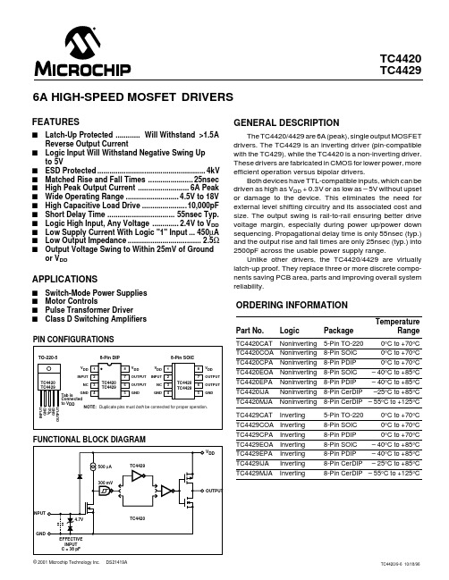
TC4420TC44296A HIGH-SPEED MOSFET DRIVERSORDERING INFORMATIONTemperaturePart No.LogicPackageRangeTC4420CAT Noninverting 5-Pin TO-2200°C to +70°C TC4420COA Noninverting 8-Pin SOIC 0°C to +70°C TC4420CPA Noninverting 8-Pin PDIP 0°C to +70°C TC4420EOA Noninverting 8-Pin SOIC – 40°C to +85°C TC4420EPA Noninverting 8-Pin PDIP – 40°C to +85°C TC4420IJA Noninverting 8-Pin CerDIP –25°C to +85°C TC4420MJA Noninverting 8-Pin CerDIP – 55°C to +125°C TC4429CAT Inverting 5-Pin TO-2200°C to +70°C TC4429COA Inverting 8-Pin SOIC 0°C to +70°C TC4429CPA Inverting 8-Pin PDIP 0°C to +70°C TC4429EOA Inverting 8-Pin SOIC – 40°C to +85°C TC4429EPA Inverting 8-Pin PDIP – 40°C to +85°C TC4429IJA Inverting 8-Pin CerDIP – 25°C to +85°C TC4429MJAInverting8-Pin CerDIP – 55°C to +125°CFEATURESs Latch-Up Protected ............ Will Withstand >1.5A Reverse Output Currents Logic Input Will Withstand Negative Swing Up to 5Vs ESD Protected.....................................................4kV s Matched Rise and Fall Times ......................25nsec s High Peak Output Current .........................6A Peak s Wide Operating Range ..........................4.5V to 18V s High Capacitive Load Drive ......................10,000pF s Short Delay Time .................................55nsec Typ.s Logic High Input, Any Voltage .............2.4V to V DD s Low Supply Current With Logic "1" Input...450µA s Low Output Impedance....................................2.5ΩsOutput Voltage Swing to Within 25mV of Ground or V DDAPPLICATIONSs Switch-Mode Power Supplies s Motor Controlss Pulse Transformer Driver sClass D Switching AmplifiersGENERAL DESCRIPTIONThe TC4420/4429 are 6A (peak), single output MOSFET drivers. The TC4429 is an inverting driver (pin-compatible with the TC429), while the TC4420 is a non-inverting driver.These drivers are fabricated in CMOS for lower power, more efficient operation versus bipolar drivers.Both devices have TTL-compatible inputs, which can be driven as high as V DD + 0.3V or as low as – 5V without upset or damage to the device. This eliminates the need for external level shifting circuitry and its associated cost and size. The output swing is rail-to-rail ensuring better drive voltage margin, especially during power up/power down sequencing. Propagational delay time is only 55nsec (typ.)and the output rise and fall times are only 25nsec (typ.) into 2500pF across the usable power supply range.Unlike other drivers, the TC4420/4429 are virtually latch-up proof. They replace three or more discrete compo-nents saving PCB area, parts and improving overall system reliability.FUNCTIONAL BLOCK DIAGRAMPIN CONFIGURATIONS6A HIGH-SPEED MOSFET DRIVERSTC4420TC4429ELECTRICAL CHARACTERISTICS: T A = +25°C with 4.5V ≤ V DD ≤ 18V, unless otherwise specified.SymbolParameterTest Conditions MinTypMaxUnitInput V IH Logic 1 High Input Voltage 2.4 1.8—V V ILLogic 0 Low Input Voltage — 1.30.8V V IN (Max)Input Voltage Range – 5—V DD +0.3V I IN Input Current0V ≤ V IN ≤ V DD– 10—10µA Output V OH High Output Voltage See Figure 1V DD – 0.025——V V OL Low Output VoltageSee Figure 1——0.025V R O Output Resistance, High I OUT = 10 mA, V DD = 18V — 2.1 2.8ΩR O Output Resistance, Low I OUT = 10 mA, V DD = 18V — 1.5 2.5ΩI PK Peak Output Current V DD = 18V (See Figure 5)—6—A I REVLatch-Up ProtectionDuty Cycle ≤ 2% 1.5——AWithstand Reverse Currentt ≤ 300µsecSwitching Time (Note 1)t R Rise Time Figure 1, C L = 2500pF —2535nsec t F Fall Time Figure 1, C L = 2500pF —2535nsec t D1Delay Time Figure 1—5575nsec t D2Delay Time Figure 1—5575nsec Power Supply I S Power Supply Current V IN = 3V —0.45 1.5mA V IN = 0V—55150µA V DDOperating Input Voltage4.5—18VABSOLUTE MAXIMUM RATINGS*Supply Voltage.........................................................+20V Input Voltage...............................................– 5V to > V DD Input Current (V IN > V DD ).........................................50mA Power Dissipation, (T A ≤ 70°C)PDIP ...............................................................730mW SOIC...............................................................470mW CerDIP............................................................800mW 5-Pin TO-220......................................................1.6W Package Power Dissipation, T C ≤ 25°C5-Pin TO-220 (With Heat Sink).........................12.5W Derating Factors (To Ambient)PDIP .............................................................8mW/°C SOIC.............................................................4mW/°C CerDIP.......................................................6.4mW/°C 5-Pin TO-220..............................................12mW/°C Thermal Impedances (To Case)5-Pin TO-220 R θJ-C ......................................................10°C/WStorage Temperature Range ................– 65°C to +150°C Operating Temperature (Chip)..............................+150°C Operating Temperature Range (Ambient)C Version...............................................0°C to +70°C I Version ...........................................– 25°C to +85°C E Version ..........................................– 40°C to +85°C M Version .......................................– 55°C to +125°C Lead Temperature (Soldering, 10 sec).................+300°C*Static-sensitive device. Unused devices must be stored in conductive material. Protect devices from static discharge and static fields.Stresses above those listed under "Absolute Maximum Ratings" may cause permanent damage to the device. These are stress ratings only and functional operation of the device at these or any other conditions above those indicated in the operation sections of the specifications is not implied. Exposure to absolute maximum rating conditions for extended periods may affect device reliability.6A HIGH-SPEED MOSFET DRIVERSTC4420TC4429ELECTRICAL CHARACTERISTICS: Measured over operating temperature range with 4.5V ≤ V DD ≤ 18V,unless otherwise specified.SymbolParameterTest Conditions MinTypMaxUnitInput V IH Logic 1 High Input Voltage 2.4——V V ILLogic 0 Low Input Voltage ——0.8V V IN (Max)Input Voltage Range – 5—V DD + 0.3V I IN Input Current0V ≤ V IN ≤ V DD– 10—10µA Output V OH High Output Voltage See Figure 1V DD – 0.025——V V OL Low Output VoltageSee Figure 1——0.025V R O Output Resistance, High I OUT = 10mA, V DD = 18V —35ΩR OOutput Resistance, LowI OUT = 10mA, V DD = 18V —2.35ΩSwitching Time (Note 1)t R Rise Time Figure 1, C L = 2500pF —3260nsec t F Fall Time Figure 1, CL = 2500pF —3460nsec t D1Delay Time Figure 1—50100nsec t D2Delay Time Figure 1—65100nsec Power Supply I S Power Supply Current V IN = 3V —0.453mA V IN = 0V—60400µA V DDOperating Input Voltage4.5—18VNOTE: 1. Switching times guaranteed by design.Figure 1. Switching Time Test Circuit6A HIGH-SPEED MOSFET DRIVERSTC4420TC4429TYPICAL CHARACTERISTICS60402010100010,000CAPACITIVE LOAD (pF)T I M E (n s e c )Fall Time vs. Capacitive Load8010050403020100–60–202060100140T A (°C)D E L A Y T I M E (n s e c )Propagation Delay Timevs. Temperature100100010,000CAPACITIVE LOAD (pF)S U P P L Y C U R R EN T (m A )Supply Current vs. Capacitive Load84705642281465605550454035D E L A Y T I M E (n s e c )4681012141618SUPPLY VOLTAGE (V)Propagation Delay Time vs. Supply Voltaget D2t D160402010100010,000CAPACITIVE LOAD (pF)Rise Time vs. Capacitive Load80100T I M E (n s e c )100100100010,000FREQUENCY (kHz)S U P P L Y C U R R E N T (m A )Supply Current vs. Frequency101000–60–202060100140T A (°C)V (V)DD5791113155040302010T I M E (n s e c )Rise and Fall Times vs. TemperatureV (V)DD120100806040200T I M E (n s e c )Rise Time vs. Supply VoltageT I M E (n s e c )Fall Time vs. Supply Voltage6A HIGH-SPEED MOSFET DRIVERSTC4420TC44292.521.515913V (V)DDLow-State Output ResistanceR ( )ΩO U T711152001601208040D E L A Y T I M E (n s e c )567111315Effect of Input Amplitudeon Propagation Delay89101214V (V)DD567111315Total nA •S Crossover*89101214SUPPLY VOLTAGE (V)5913V (V)DDHigh-State Output ResistanceR ( )ΩO U T 71115The values on this graph representthe loss seen by the driver during one complete cycle. For a single transition, divide the value by 2.*TYPICAL CHARACTERISTICS (Cont.)6A HIGH-SPEED MOSFET DRIVERS TC4420TC44296A HIGH-SPEED MOSFET DRIVERSTC4420TC4429Information contained in this publication regarding device applications and the like is intended through suggestion only and may be superseded by updates. It is your responsibility to ensure that your application meets with your specifications. No representation or warranty is given and no liability is assumed by Microchip Technology Incorporated with respect to the accuracy or use of such information, or infringement of patents or other intellectual property rights arising from such use or otherwise. Use of Microchipís products as critical components in life support systems is not authori zed except with express written approval by Microchip. No licenses are conveyed, implicitly or otherwise, except as maybe explicitly expressed herein, under any intellec-tual property rights. The Microchip logo and name are registered trademarks of Microchip Technology Inc. in the U.S.A. and other countries. All rights reserved. All other trademarks mentioned herein are the property of their respective companies.All rights reserved. © 2001 Microchip Technology Incorporated. Printed in the USA. 1/01Printed on recycled paper.AMERICASCorporate Office2355 West Chandler Blvd.Chandler, AZ 85224-6199Tel: 480-792-7200 Fax: 480-792-7277Technical Support: 480-792-7627Web Address: Rocky Mountain2355 West Chandler Blvd.Chandler, AZ 85224-6199Tel: 480-792-7966 Fax: 480-792-7456Atlanta500 Sugar Mill Road, Suite 200B Atlanta, GA 30350Tel: 770-640-0034 Fax: 770-640-0307AustinAnalog Product Sales8303 MoPac Expressway North Suite A-201Austin, TX 78759Tel: 512-345-2030 Fax: 512-345-6085Boston2 Lan Drive, Suite 120Westford, MA 01886Tel: 978-692-3848 Fax: 978-692-3821BostonAnalog Product SalesUnit A-8-1 Millbrook Tarry Condominium 97 Lowell RoadConcord, MA 01742Tel: 978-371-6400 Fax: 978-371-0050Chicago333 Pierce Road, Suite 180Itasca, IL 60143Tel: 630-285-0071 Fax: 630-285-0075Dallas4570 Westgrove Drive, Suite 160Addison, TX 75001Tel: 972-818-7423 Fax: 972-818-2924DaytonTwo Prestige Place, Suite 130Miamisburg, OH 45342Tel: 937-291-1654 Fax: 937-291-9175DetroitTri-Atria Office Building32255 Northwestern Highway, Suite 190Farmington Hills, MI 48334Tel: 248-538-2250 Fax: 248-538-2260Los Angeles18201 Von Karman, Suite 1090Irvine, CA 92612Tel: 949-263-1888 Fax: 949-263-1338Mountain ViewAnalog Product Sales 1300 Terra Bella AvenueMountain View, CA 94043-1836Tel: 650-968-9241 Fax: 650-967-1590New York150 Motor Parkway, Suite 202Hauppauge, NY 11788Tel: 631-273-5305 Fax: 631-273-5335San JoseMicrochip Technology Inc.2107 North First Street, Suite 590San Jose, CA 95131Tel: 408-436-7950 Fax: 408-436-7955Toronto6285 Northam Drive, Suite 108Mississauga, Ontario L4V 1X5, Canada Tel: 905-673-0699 Fax: 905-673-6509ASIA/PACIFICChina - BeijingMicrochip Technology Beijing Office Unit 915New China Hong Kong Manhattan Bldg.No. 6 Chaoyangmen Beidajie Beijing, 100027, No. ChinaTel: 86-10-85282100 Fax: 86-10-85282104China - ShanghaiMicrochip Technology Shanghai Office Room 701, Bldg. BFar East International Plaza No. 317 Xian Xia Road Shanghai, 200051Tel: 86-21-6275-5700 Fax: 86-21-6275-5060Hong KongMicrochip Asia PacificRM 2101, Tower 2, Metroplaza 223 Hing Fong RoadKwai Fong, N.T., Hong KongTel: 852-2401-1200 Fax: 852-2401-3431IndiaMicrochip Technology Inc.India Liaison Office Divyasree Chambers 1 Floor, Wing A (A3/A4)No. 11, O íShaugnessey Road Bangalore, 560 025, IndiaTel: 91-80-2290061 Fax: 91-80-2290062JapanMicrochip Technology Intl. Inc.Benex S-1 6F3-18-20, Shinyokohama Kohoku-Ku, Yokohama-shi Kanagawa, 222-0033, JapanTel: 81-45-471- 6166 Fax: 81-45-471-6122KoreaMicrochip Technology Korea 168-1, Youngbo Bldg. 3 Floor Samsung-Dong, Kangnam-Ku Seoul, KoreaTel: 82-2-554-7200 Fax: 82-2-558-5934ASIA/PACIFIC (continued)SingaporeMicrochip Technology Singapore Pte Ltd.200 Middle Road #07-02 Prime Centre Singapore, 188980Tel: 65-334-8870 Fax: 65-334-8850TaiwanMicrochip Technology Taiwan 11F-3, No. 207Tung Hua North Road Taipei, 105, TaiwanTel: 886-2-2717-7175 Fax: 886-2-2545-0139EUROPEAustraliaMicrochip Technology Australia Pty Ltd Suite 22, 41 Rawson Street Epping 2121, NSW AustraliaTel: 61-2-9868-6733 Fax: 61-2-9868-6755DenmarkMicrochip Technology Denmark ApS Regus Business Centre Lautrup hoj 1-3Ballerup DK-2750 DenmarkTel: 45 4420 9895 Fax: 45 4420 9910FranceArizona Microchip Technology SARL Parc d íActivite du Moulin de Massy 43 Rue du Saule Trapu Batiment A - ler Etage 91300 Massy, FranceTel: 33-1-69-53-63-20 Fax: 33-1-69-30-90-79GermanyArizona Microchip Technology GmbH Gustav-Heinemann Ring 125D-81739 Munich, GermanyTel: 49-89-627-144 0 Fax: 49-89-627-144-44GermanyAnalog Product Sales Lochhamer Strasse 13D-82152 Martinsried, GermanyTel: 49-89-895650-0 Fax: 49-89-895650-22ItalyArizona Microchip Technology SRL Centro Direzionale ColleoniPalazzo Taurus 1 V. Le Colleoni 120041 Agrate Brianza Milan, ItalyTel: 39-039-65791-1 Fax: 39-039-6899883United KingdomArizona Microchip Technology Ltd.505 Eskdale Road Winnersh Triangle WokinghamBerkshire, England RG41 5TUTel: 44 118 921 5869Fax: 44-118 921-582001/09/01。
TC4420IPA中文资料
DC CHARACTERISTICS
Electrical Specifications: Unless otherwise noted, TA = +25°C with 4.5V ≤ VDD ≤ 18V.
Parameters
Sym
Min
Typ Max Units
Conditions
Input
Logic ‘1’, High Input Voltage
Applications
• Switch-Mode Power Supplies • Motor Controls • Pulse Transformer Driver • Class D Switching Amplifiers
General Description
The TC4420/TC4429 are 6A (peak), single-output MOSFET drivers. The TC4429 is an inverting driver (pin-compatible with the TC429), while the TC4420 is a non-inverting driver. These drivers are fabricated in CMOS for lower power and more efficient operation versus bipolar drivers.
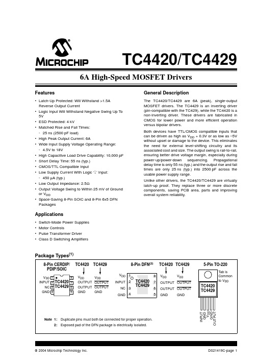
Package Types(1)
8-Pin CERDIP/ TC4420 TC4429 PDIP/SOIC
VDD 1
8
INPUT 2 TC4420 7
NC 3 TC4429 6
GND 4
5
VDD
VDD