REC5-0509DRWH2中文资料
Recom RP100H-RW DC DC 转换器产品说明书
FeaturesRegulated Converter• 4:1 wide input range• 3kVAC reinforced insulation for 110Vin 2.25kVDC basic insulation for 24Vin & 48Vin • Efficiency up to 93%• No minimum load required• EN50155, IEC/EN60950-1 & UL60950-1 certifiedDescriptionThe half-brick RP100H series DC/DC converters are designed for railway rolling stock and high voltage battery applications. Each series has three 4:1 input voltage range options to cover all input voltages from 9VDC up to 160VDC with isolated and regulated 5V to 48VDC outputs. The converters have high efficiencies and metal base-RP100H-RW DC/DC Converter100 Watt Half BrickEN50155 certifiedIEC/EN60950-1 certified UL60950-1 certifiedE196683RP100H-2415SRW 9-36 15 6700 4601 100 91 4460RP100H-2424SRW 9-36 24 4200 4666 101 90 1750RP100H-2448SRW 9-36 48 2100 4666 101 90 430RP100H-4805SRW 16.5-75 5 20000 2240 100 93 40000RP100H-4812SRW 16.5-75 12 8400 2333 101 90 7000RP100H-4815SRW 16.5-75 15 6700 2300 100 91 4460RP100H-4824SRW 16.5-75 24 4200 2333 101 90 1750RP100H-4848SRW 16.5-75 48 2100 2307 101 90 430RP100H-11005SRW 43-160 5 20000 1010 100 93 40000RP100H-11012SRW 43-160 12 8400 1018 101 90 7000RP100H-11015SRW 43-160 15 6700 1015 100 91 4460RP100H-11024SRW 43-160 24 4200 1018 101 90 1750RP100H-11048SRW 43-160 48 2100 1007 101 90 430Ordering ExamplesRP100H-2405SRW/N = 24V Input, 5V Output, Single, Neg. CTRL function RP100H-11012SRW/P = 110V Input, 12V Output, Single, Pos. CTRL functionRP100H-2405SRW/N-HC = 24V Input, 5V Output, Single, Neg. CTRL function, premounted Heat-sinkModel NumberingInput Voltage Output VoltageS ingleRP100H-__ __SRW/_ _Notes:Note2: standard part is with suffix “P” for positive logic (1=ON, 0=OFF) or add suffix “N” instead for negative logic (0=ON, 1=OFF) Note3: add suffix “-HC” for premounted Heat-sink CTRL Logic (2)Package (3)Notes:Note1:Efficiency is tested by nominal Vin, full load and at 25°Chttps:///pdf/Powerline_DC-DC/RSPxxx-168.pdf/eval-ref-boardsSpecifications (measured @Ta = 25°C, resistive load, nominal Vin and rated Iout unless otherwise noted)Specifications (measured @Ta = 25°C, resistive load, nominal Vin and rated Iout unless otherwise noted)RP100H-4805SRW708090100Efficiency vs. Output CurrentPower up Start-up CharacteristicON/OFF Control Start-up Rise CharacteristicSpecifications (measured @Ta = 25°C, resistive load, nominal Vin and rated Iout unless otherwise noted)Efficiency vs. Input Voltage60708090100708010090RP100H-11005SRWEfficiency vs. Output CurrentPower up Start-up CharacteristicSpecifications (measured @Ta = 25°C, resistive load, nominal Vin and rated Iout unless otherwise noted)OUTPUT TRIM Typical Output Ripple and NoisePower up Start-up CharacteristicOutput Voltage TrimmingRP100H-RW converters offer the feature of trimming the output voltage over a certain range around the nominal value by using external trim resistors. The values for trim resistors shown in trim tables below are according to standard E96 values; therefore, the specified voltage may slightly vary; they also can be calculated with below shown equation.TRIM DOWNTRIM UPTRIM-Sense+SenseSpecifications (measured @Ta = 25°C, resistive load, nominal Vin and rated Iout unless otherwise noted)OUTPUT TRIMRP100H-xx05SRWRP100H-xx12SRWRP100H-xx15SRWRP100H-xx24SRWRP100H-xx48SRWTrim Down all Vout‘sTrim up 12345678910%Vout = 5.05 5.10 5.15 5.20 5.25 5.30 5.35 5.4 5.45 5.50Volts R 1 = 30915810578.763.453.646.440.236.533.2kOhms Trim up 12345678910%Vout =12.1212.2412.3612.4812.6012.7212.8412.9613.0813.20Volts R 1 = 88745330122618215413311810595.3kOhms Trim up 12345678910%Vout =15.1515.3015.4515.6015.7515.9016.0516.2016.3516.50Volts R 1 = 1130576383294237196169150137124kOhms Trim up 12345678910%Vout =24.2424.4824.7224.9625.2025.4425.6825.9226.1626.40Volts R U = 1870953634487392324280249226205kOhms Trim up 12345678910%Vout =48.4848.9649.4449.9250.4050.8851.3651.8452.3252.80Volts R 1 = 3830196013001000806681576511464422kOhms Trim down 12345678910%R 2 = 97.647.531.623.217.814.712.110.59.098.06kOhms Trim down 11121314151617181920%R 2 =7.156.345.765.114.644.223.923.573.243.01kOhmsTrim CalculationVout = Output VoltageR 1 =100*Vout+D Vout * Vout)- (100+2D Vout) k Ω D Vout = Output Voltage Trim in %1.225*D Vout D VoutR1 =trim up resistorR2 = trim down resistor R 2 = 100 - 2 k ΩD Vout Practical Example:Trim Up:Vout = 5V, D Vout = 10% (5.5V)R 1 =100*Vout+D Vout * Vout) - (100+2D Vout) k Ω = 100*5 +10*5 - 100+2*10= 44.89 - 12 = 32.9k Ω 1.225*D Vout D Vout 1.225*10 10Trim down:Vout = 5V, D Vout = -10% (4.5V)R 2 = 100 - 2 k Ω = 100 - 2 = 8.06k ΩD Vout 10Specifications (measured @Ta = 25°C, resistive load, nominal Vin and rated Iout unless otherwise noted)REGULATIONSParameter Condition ValueOutput Accuracy±1.0%Line Regulation low line to high line at full load±0.1% Load Regulation0% to 100% load0.1% Transient Response25% load step change200µs typ.; 250µs max.Transient Response to Dynamic Load Change from 100% to 75% to 100% of Full Load at nom.VinRP100H-4805SRWRP100H-2405SRWRP100H-11005SRWSpecifications (measured @Ta = 25°C, resistive load, nominal Vin and rated Iout unless otherwise noted)ENVIRONMENTALParameterCondition ValueOperating Case Temperature Range refer to derating graphMaximum Case Temperature 105°CTemperature Coefficient ±0.02%/°C max.Thermal Impedance vertical direction by natural convection (0.1m/s) without Heat-sink vertical direction by natural convection (0.1m/s) with Heat-sink6.7°C/W 4.7°C/W Operating Humidity 5% - 95% RHPollution Degree PD2Shock according to EN61373 standard Thermal Shock according to MIL-STD-810F standardVibrationaccording to EN61373 standardFire protection on railway vehicles according to EN45545-2, 2013 standardMTBFaccording to MIL-HDBK-217F standard, 25°C408.7 x 103 hoursPROTECTIONSParameterConditionValueShort Circuit Protection (SCP)below 100m Ωcontinuous, automatic recovery Over Voltage Protection (OVP)% of nom. Vout115%-130%, Hiccup Mode Over Load Protection (OLP)% Iout rated24Vin, 48Vin 110Vin120%-150%, Hiccup Mode 150% typ., Hiccup ModeOver Temperature Protection (OTP)+110°C to +120°C Isolation Voltage110VinI/P to O/P I/P or O/P to Case 3kVAC/1minute 1.5kVAC/1minute 24Vin, 48VinI/P to O/P I/P or O/P to Case2.25kVDC/1minute 1.6kVDC/1minuteIsolation Resistance 500 VDC1G Ω min.Isolation Capacitance 2500pF max.Isolation Grade110 Vin 24Vin, 48Vin reinforced insulationbasic insulationThermal CalculationNotes:Note4: Refer to local wiring regulations if input over-current protection is also required. Recommended fuse: T35A slow blow.R thcase-ambient = 6.7°C/W (vertical) T case = Case Temperature R thcase-ambientHC = 4.7°C/W (vertical) T ambient = Environment Temperature P dissipation = Internal lossesR thcase-ambient = T case - T ambientP IN = Input PowerP dissipationP OUT = Output Power h = Efficiency under given Operating ConditionsP dissipation = P IN - P OUT = P OUTapp- P OUTapp R thcase-ambient = Thermal Impedance h Practical Example:Take the RP100H-2405SRW with 9V input Voltage and 50% load. What is the maximum ambient operating temperature? Use converter vertical in application without airflow.Eff min = 91% @ V nomP OUT = 100W P OUTapp = 100 x 0.5 = 50W h = 91% (Efficiency vs. Load Graph)without Heat-sink with Heat-sinkR th = T casemax - T amb --> 6.7°C/W = 105-T amb R thHC = T casemax - T amb--> 4.7°C/W = 105-T amb P dissipation 4.95W P dissipation4.95W T amb = 72°C T ambHC = 82°CSpecifications (measured @Ta = 25°C, resistive load, nominal Vin and rated Iout unless otherwise noted)Specifications (measured @Ta = 25°C, resistive load, nominal Vin and rated Iout unless otherwise noted)DC/DC ConverterSpecifications (measured @Ta = 25°C, resistive load, nominal Vin and rated Iout unless otherwise noted)RP100H-RWSeriesConducted Emission EN55022 Class AConducted Emission EN55022 Class AC4C5C6C7C8Shield PlaneL1C18+V INEMI Filtering according to EN55022/11 Class A and EN50121-1 (110Vin)DC/DC ConverterSpecifications (measured @Ta = 25°C, resistive load, nominal Vin and rated Iout unless otherwise noted)RP100H-RWSeriescontinued on next pageEMI Filtering according to EN55022/11 Class B (24Vin and 48Vin)Shield Plane100-110xxSRW, Class BNNC6C9C8C3C4CaseL2C7C19C20Shield PlaneC12C13C14C10C11C16C2C4L1L2C5C8C6C7C11C3Conducted Emission EN55022 Class ADC/DC ConverterSpecifications (measured @Ta = 25°C, resistive load, nominal Vin and rated Iout unless otherwise noted)RP100H-RWSeriesEMI Filtering according to EN55022/11 Class B (110Vin)C8Shield PlaneShield PlaneC9C1C2C3C11C12C10CaseL1C4C5C8C13C14C17C9C19C3C4L1L2C12C10C11C15C15Shield PlaneC9C10C12Conducted Emission EN55022 Class BSpecifications (measured @Ta = 25°C, resistive load, nominal Vin and rated Iout unless otherwise noted)Specifications (measured @Ta = 25°C, resistive load, nominal Vin and rated Iout unless otherwise noted)The product information and specifications may be subject to changes even without prior written notice.The product has been designed for various applications; its suitability lies in the responsibility of each customer. The products are not authorized for use in safety-critical applications without RECOM’s explicit written consent. A safety-critical application is an application where a failure may reasonably be expected to endanger or cause loss of life, inflict bodily harm or damage property. The applicant shall indemnify and hold harmless RECOM, its affiliated companies and its representatives against any damage claims in connection with the unauthorizeduse of RECOM products in such safety-critical applications.PACKAGING INFORMATIONParameterTypeValuePackaging Dimension traywithout Heat-sink with Heat-sink157.0 x 88.0 x 12.8mm 157.0 x 88.0 x 24.8mmPackaging Quantity 2pcs.Storage Temperature Range -55°C to +125°C Storage Humidity5% - 95% RH。
常用三极管参数大全
玉林万顺达电脑芯片级维修资料 2010-07-20整理玉林万顺达电脑芯片级维修资料 2010-07-20整理玉林万顺达电脑芯片级维修资料 2010-07-20整理玉林万顺达电脑芯片级维修资料 2010-07-20整理玉林万顺达电脑芯片级维修资料 2010-07-20整理玉林万顺达电脑芯片级维修资料 2010-07-20整理玉林万顺达电脑芯片级维修资料 2010-07-20整理玉林万顺达电脑芯片级维修资料 2010-07-20整理玉林万顺达电脑芯片级维修资料 2010-07-20整理玉林万顺达电脑芯片级维修资料 2010-07-20整理玉林万顺达电脑芯片级维修资料 2010-07-20整理玉林万顺达电脑芯片级维修资料 2010-07-20整理玉林万顺达电脑芯片级维修资料 2010-07-20整理玉林万顺达电脑芯片级维修资料 2010-07-20整理玉林万顺达电脑芯片级维修资料 2010-07-20整理玉林万顺达电脑芯片级维修资料 2010-07-20整理玉林万顺达电脑芯片级维修资料 2010-07-20整理玉林万顺达电脑芯片级维修资料 2010-07-20整理玉林万顺达电脑芯片级维修资料 2010-07-20整理玉林万顺达电脑芯片级维修资料 2010-07-20整理玉林万顺达电脑芯片级维修资料 2010-07-20整理玉林万顺达电脑芯片级维修资料 2010-07-20整理玉林万顺达电脑芯片级维修资料 2010-07-20整理玉林万顺达电脑芯片级维修资料 2010-07-20整理玉林万顺达电脑芯片级维修资料 2010-07-20整理玉林万顺达电脑芯片级维修资料 2010-07-20整理玉林万顺达电脑芯片级维修资料 2010-07-20整理玉林万顺达电脑芯片级维修资料 2010-07-20整理玉林万顺达电脑芯片级维修资料 2010-07-20整理玉林万顺达电脑芯片级维修资料 2010-07-20整理。
WDH-31-200中文说明书1105A-2011年之前版本
(1)保护功能:装置具有过载(反时限特性)、欠载、起动加速超时、起动过流、运行过流(堵转)、电流不平衡、断相、过压、欠压等保护功能。用户可现场设置: 电动机起动时间、额定电流、过载动作曲线、欠载动作值、过压动作值、欠压动作值、起动过流/运行过流(堵转)电流倍数(相对于额定电流)、漏电保护动作电流值、电流不平衡动作值。
4.通讯协议………………………………………………………13
5.产品规格选择表………………………………………………15
6.订货须知………………………………………………………16
附录:参数通信地址表…………………………………………17
1.概述
1.1简介:
WDH-31-200是江苏斯菲尔电气股份有限公司推出的集保护、测量、变送、通讯等功能于一体的微机电动机保护装置,精度2 级以上,功能稳定可靠。
“MENU”键 :在整定状态下,长按“MENU”键,仪表显示“SAVE”
菜单;单击“MENU”键返回到上一个整定参数;在故障记录界面下,单击“MENU”键,返回到正常状态;在“ ”界面,单击“MENU”键,返回正常状态;
“ ”键 :在整定状态下,按“ ”键,进入下一个参数设置界面;保护动作后,按“ ”键保护输出触点复位;
在正常运行时,按“ ”键暂停电流值循环显示,只显示当前某相电流值,再按“ ”键,恢复电流值循环显示。
2.3操作及显示说明
保护装置上电后,LCD显示“ ”;电动机起动后LCD显示“ ”,起动结束后(根据用户整定的电动机起动时间),进入运行状态,LCD循环显示A、B、C三相电流值和辅助电源电压值,按“ ”键固定显示某相电流值或辅助电源值; 在此前提下,按“ ”或“ ”键,可以选择要固定显示的数据;再按“ ”键,则恢复三相电流值和辅助电源电压值的循环显示。
API-5LD中文版
抗腐蚀合金复合钢管或衬管规范API 5LD规范第二版1998年7月生效日期:1998年12月31日特别说明API出版物仅对普遍性问题做出了规定。
对一些特殊情况,应查阅联邦、州和地方的有关法规。
API不为供应商、制造商和雇主承担其雇员在健康、安全风险及预防措施进行教育、培训和装备等方面的义务。
亦不承担他们因违反联邦、州和地方法律而应负的责任。
有关健康、安全风险及预防措施方面的详细资料或情况可向雇主、供应商或制造商索取,或从材料的安全数据表处得到。
API出版物不能以任何方式解释为授予任何人权利不制造、销售或使用属于专利证书所涉及的方法、设备或产品。
同样不能解释为保证任何人因侵犯专利权而不承担责任。
一般情况下,API标准每5年至少进行一次复审、修改、重新确认或予以撤销。
有时审定周期会延长,延长期不超过两年。
所以,除已授权再版延期外,作为现行的API标准自出版之日起,5年后不再有效。
可向API勘探开发部[电话:(202)6828000]了解本出版物情况。
API每年颁布一次出版物和资料目录,每季度订正一次变动情况,API地址位于:American Petroleum Institute,1220,L Street,N.W.Washington,D.C.20005。
本文件是在保证获得适当通知和参与开发工作的基础上,根据API标准化程序制定的,称之为API标准。
涉及到本标准内容的解释和本标准制定程序的问题,请直接致函美国石油学会勘探开发部部长。
地址:American Petroleum Institute,1220,L Street,N.W.Washington,D.C.20005。
要求复制或翻译本资料全文或任一部分也可致函商务部长。
API标准的出版便于已被证实的安全可靠的技术工艺及具体做法的推广应用。
考虑到这些标准的使用时间和地点,这些标准无意排除对采用可靠技术方法的需求。
API标准的制定和出版无意以任何方式禁止任何人采用其它标准。
R9说明书
是IP-COM Trade Mark Holder注册商标。
这里提及的其它产品和产品名称均是此公司所属的商标或注册商标。
本产品的所有部分(包括配件和软件),其版权属于IP-COM Trade Mark Holder所有,在未经过IP-COM Trade Mark Holder许可的情况下,不得任意拷贝、抄袭、仿制或翻译。
本手册中的所有图片和产品规格参数仅供参考,随着软件或硬件的升级会略有差异,如有变更,恕不另行通知。
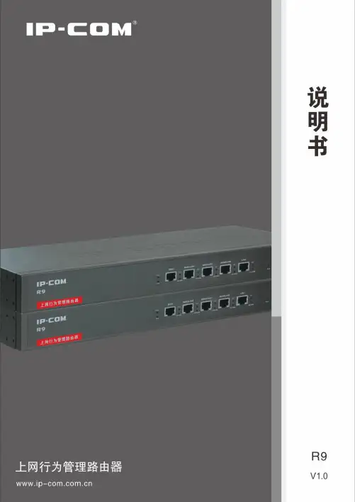
如需了解更多产品信息,请浏览我们的网站:目录第一章产品介绍 (2)1.1产品简介 (2)1.2主要特性 (2)1.3产品规格 (3)1.4包装清单 (4)1.5硬件描述 (5)1.6系统需求 (6)1.7安装环境要求 (6)第二章快速安装指南 (7)2.1硬件安装步骤 (7)2.2配置计算机网络设置 (7)2.3配置路由器设置 (13)第三章路由器详细设置 (17)3.1系统状态 (17)3.2设置向导 (20)3.3网络参数 (20)3.4过滤设置 (30)3.5安全设置 (40)3.6高级设置 (44)3.7VPN设置 (52)3.8系统监控 (73)3.9系统工具 (75)附录:常用命令介绍 (79)第一章产品介绍1.1 产品简介IP-COM企业/网吧安全网关—R9,专为中小企业、政府机关、教育及科研机构等用户设计,是具备“上网行为管理”和“多WAN路由器”双重功能的新一代硬件网络接入设备。
多线路负载均衡和弹性带宽可以保证网络的合理利用;上网行为管理和防火墙的安全功能可以帮助企业对员工访问Internet的行为进行限制和管理;VPN功能可以帮助远程用户,公司分支机构,商业伙伴及供应商同公司的内部网建立可信的安全连接,保证数据的安全传输。
总之R9是一款可以轻松解决带宽,网络管理和安全等问题的高端企业/网吧安全网关。
1.2主要特性符合IEEE 802.3、IEEE 802.3u、IEEE 802.3ab、IEEE 802.3x等标准高达550MHz的CPU处理能力,超强NAT转发性能,允许更多用户接入支持多线接入,自动实现带宽叠加、智能负载均衡(也可设置一定比例负载均衡) 支持弹性带宽,最大化的利用带宽资源提供1个10/100M/1000M自适应以太网(WAN)接口,连接外部网络提供3个10/100M/1000M自适应以太网(WAN/LAN)接口,可根据需要灵活切换为WAN/LAN口提供1个10/100M/1000M自适应以太网(LAN)接口,连接内部局域网支持LAN/WAN口访问控制,允许指定地址的主机通过SSL的方式管理路由器内建DHCP服务器,可进行静态地址分配支持MAC地址克隆,可以克隆当前PC的MAC地址支持端口模式,用户可根据需要选择不同的WAN口协商模式支持端口镜像,便于网吧监控内建防火墙,可精确控制上网时间;支持客户端过滤、MAC过滤、URL过滤支持网址分类过滤,更方便对域名的管理支持IP-MAC地址绑定功能,有效防止ARP攻击、ARP欺骗和非授权用户接入 支持攻击防御,保证网络安全稳定支持多组虚拟服务器、DMZ主机支持UPnP、DDNS(动态域名解析) 和静态路由支持电子公告功能,用户第一次打开网页时弹出公告内容支持即插即用功能,用户配置任意IP均能实现上网功能支持邮件密送功能,便于监控邮件支持地址伪装功能,可实现路由器LAN口下不同网段的PC上网支持PPTP/L2TP/IPsec VPN服务器功能,支持8组用户同时接入提供系统日志和流量统计功能支持配置文件备份与恢复1.3 产品规格支持的标准和协议IEEE 802.3、IEEE 802.3u、IEEE 802.3ab、IEEE 802.3x、TCP/IP、DHCP、ARP、NAT、PPPoE、SNTP、HTTP、DNS、ICMP网络介质10Base-T:3类或3类以上UTP 100Base-TX:5类UTP1000Base-T:超5类UTP端口和LED指示灯WAN/LAN口3个“WAN/LAN”指示灯和3个“1000M”指示灯WAN口1个“WAN”指示灯和1个“1000M”指示灯LAN口1个“LAN”指示灯和1个“1000M”指示灯其它Power(电源指示灯)、SYS(系统状态指示灯)外形尺寸(L x W x H)440mm×209mm×44mm使用环境工作温度:0℃到45℃;存储温度:-30℃到70℃;工作湿度:10%到90% RH无凝结;存储湿度:10%到90% RH无凝结;电源及功耗输入:AC 220V 50Hz功耗:最大4W1.4 包装清单在包装盒完整的情况下,开启包装盒。
REC5-4812DRW中文资料
元器件交易网
ECONOLINE - DC/DC-Converter
元器件交易网
ECONOLINE - DC/DC-Converter
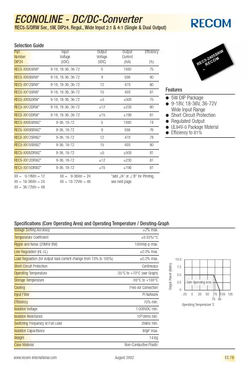
REC5-S/DRW Ser., 5W, DIP24, Regul., Wide Input 2:1 & 4:1 (Single & Dual Output) Selection Guide
Part Number DIP24 REC5-XX05SRW* REC5-XX09SRW* REC5-XX12SRW* REC5-XX15SRW* REC5-XX05DRW* REC5-XX12DRW* REC5-XX15DRW* REC5-XX05SRWZ* REC5-XX09SRWZ* REC5-XX12SRWZ* REC5-XX15SRWZ* REC5-XX05DRWZ* REC5-XX12DRWZ* REC5-XX15DRWZ* XX = 9-18Vin = 12 XX = 18-36Vin = 24 XX = 36-72Vin = 48 Input Voltage (VDC) 9-18, 18-36, 36-72 9-18, 18-36, 36-72 9-18, 18-36, 36-72 9-18, 18-36, 36-72 9-18, 18-36, 36-72 9-18, 18-36, 36-72 9-18, 18-36, 36-72 9-36, 18-72 9-36, 18-72 9-36, 18-72 9-36, 18-72 9-36, 18-72 9-36, 18-72 9-36, 18-72 XX = 9-36Vin = 24 XX = 18-72Vin = 48 Output Voltage (VDC) 5 9 12 15 ±5 ±12 ±15 5 9 12 15 ±5 ±12 ±15 Output Current (mA) 1000 556 470 400 ±500 ±230 ±190 1000 556 470 400 ±500 ±230 ±190 Efficiency (%) 75 80 80 81 75 80 81 74 76 78 80 81 81 81
大屏显示器说明书
一.概述本公司生产的LED 系列大屏幕显示器具有多种输入信号接口,适用于各种具有数字信号输出接口的称重、温度等仪表作外接显示器使用,是工矿企业和交通运输等部门作为远距离监视的合适的智能型数据显示器。
二.主要技术参数 1. 型号的意义2. 基本参数见表显示字高显示位数 外形尺寸 (mm)功 耗重 量5英寸(130mm ) 5 710(L )×195(H )×78(W )≤30VA ≤5Kg 8英寸(205mm ) 4 700(L )×280(H )×110(W )≤20VA ≤8Kg 8英寸(205mm ) 5 850(L )×275(H )×120(W )≤20VA ≤10Kg 12英寸(315mm ) 4 1026(L )×400(H )×120(W )≤40VA ≤13Kg 12英寸(315mm )51260(L )×400(H )×120(W )≤40VA ≤15Kg▲ 非标产品另行设计3. 使用工作条件及通讯参数(1)工作条件a 、电源电压:Vb 、电源频率:50±1Hzc 、环境温度:0~40℃d 、相对湿度:40℃(20~90)%RHe 、周围无腐蚀性气体或腐蚀液f 、应远离强电磁场,远离高压动力线及高频设备。
HG-2(2)通讯参数a、串行BCD码电流环通讯电流:10mA通讯距离:≤100mb、串行电流环波特率:300、600、1200 bit任选通讯电流:20mA通讯距离:≤200mc、RS 232 C波特率:300、600、1200 bit任选通讯距离:≤10md、标准模拟量输入信号:4-20mA通讯距离:≤100m注:1、用户如对波特率另有要求,请在订货时注明,可按非标订货。
2、通讯距离受现场环境的影响,可能缩短或延长。
三.安装方式及尺寸1. 安装方式:悬挂式2. 电源、通讯接口插座及保险丝的位置:出厂时一般都安装在大显示器左侧下(205为右侧下),如有特殊需要也可安装在其它位置。
R05J09中文资料
Dual Output TypesRxxG055/12±5±1007127RxxG095/12±9±557435DIP14 RxxG125/12±12±427542RxxG155/12±15±337641RxxG0524/48±5±10080/7045RxxG0924/48±9±557052/58DIP14 RxxG1224/48±12±427065/68RxxG1524/48±15±337070/75RxxH055/12±5±1007127RxxH095/12±9±557435SIP7 RxxH125/12±12±427542RxxH155/12±15±337641RxxH0524/48±5±10070/8045RxxH0924/48±9±557052/58SIP7 RxxH1224/48±12±427065/68RxxH1524/48±15±337070/75Absolute Maximum RatingsInput Voltage V IN5V types 7V typ.12V types 15V typ.24V types 24V typ.48V types48V typ.Short Circuit Duration 1)1s Internal Power Dissipation560mW Lead Temperature (1.5 mm from case for 10 seconds)300 °C1).Supply voltage must be discontinued at the end of the short circuit duration.Input Voltage Range V IN (continuous operation)5V input types 4.5VDC min./ 5.5VDC max.12V input types 10.8VDC min./ 13.2VDC max.24V input types 28VDC max.48V input types54VDC max.Reflected Ripple Current (depending on the type)20 mA p-p min.to 40 mA p-p max.Voltage Set Point Accuracy See Tolerance EnvelopeLine Regulation1.0% / 1.2% of V INLoad Voltage Regulation (10% load to 100% full load)single output types 6.7% min./ 15% max.dual output types 6.8% min./ 10% max.Ripple & Noise (20MHz band limited)single output types 32mVp-p min./ 80mVp-p max.dual output types24mVp-p min./ 40mVp-p max.Isolation Voltage (for 1 minute)3000VDC min.Test Voltage (50Hz,10 seconds)3000 Vpk min.Resistance (Viso = 1000V)10 G Ωtyp.Switching Frequency at Full Load (depending on the type)V IN 5V output types 120kHz min./ 135kHz max.V IN 12V output types 150kHz min./ 170kHz max.V IN 24V output types 150kHz max.V IN 48V output types150kHz max.Package Weight2.11 gOperating Temperature Range (all output types)–40°C min.to +85°C max.(see graph)Storage Temperature Range–50°C min.+125°C max.Case Temperature Above Ambient (depending on the type)5V output types+28°C max.all other output types +25°C max.MTTF 1) (depending on the type)–40°C,single output types 303kHrs min./ 2938kHrs max.+25°C,single output types 252kHrs min./ 2414kHrs max.+85°C,single output types 212kHrs min./ 1961kHrs max.–40°C,dual output types 185kHrs min./ 2068kHrs max.+25°C,dual output types 154kHrs min./ 1697kHrs max.+85°C,dual output types130kHrs min./ 1368kHrs max.1).Calculated using MIL-HDBK-217F with nominal input voltage at full load.Please contact us,if you need exact parameters for the converter you have selected.Electrical Specifications (measured at T A = 25°C,at nominal input voltage and rated output current unless otherwise specified)Package Style and Pinning (mm)。
噪声系数基础
Agilent Technologies Fundamentals of RF and Microwave Noise Figure Measurements Application Note 57-1Table of Contents1.What is Noise Figure? . . . . . . . . . . . . . . . . . . . . . . . . . . . . . . . . . . . .4Introduction . . . . . . . . . . . . . . . . . . . . . . . . . . . . . . . . . . . . . . . . . . . . . . . .4 The Importance of Noise in Communication Systems . . . . . . . . . . . . .5 Sources of Noise . . . . . . . . . . . . . . . . . . . . . . . . . . . . . . . . . . . . . . . . . . .6 The Concept of Noise Figure . . . . . . . . . . . . . . . . . . . . . . . . . . . . . . . . . .7 Noise Figure and Noise Temperature . . . . . . . . . . . . . . . . . . . . . . . . . .8 2.Noise Characteristics of Two-Port Networks . . . . . . . . . . . .9The Noise Figure of Multi-stage Systems . . . . . . . . . . . . . . . . . . . . . . .9 Gain and Mismatch . . . . . . . . . . . . . . . . . . . . . . . . . . . . . . . . . . . . . . . . .10 Noise Parameters . . . . . . . . . . . . . . . . . . . . . . . . . . . . . . . . . . . . . . . . . .10 The Effect of Bandwidth . . . . . . . . . . . . . . . . . . . . . . . . . . . . . . . . . . . . .11 3. The Measurement of Noise Figure . . . . . . . . . . . . . . . . . . . . . . .12Noise Power Linearity . . . . . . . . . . . . . . . . . . . . . . . . . . . . . . . . . . . . . . .12 Noise Sources . . . . . . . . . . . . . . . . . . . . . . . . . . . . . . . . . . . . . . . . . . . . .12 The Y-Factor Method . . . . . . . . . . . . . . . . . . . . . . . . . . . . . . . . . . . . . . . .13 The Signal Generator Twice-Power Method . . . . . . . . . . . . . . . . . . . . .14 The Direct Noise Measurement Method . . . . . . . . . . . . . . . . . . . . . . . .14 Corrected Noise Figure and Gain . . . . . . . . . . . . . . . . . . . . . . . . . . . . . .15 Jitter . . . . . . . . . . . . . . . . . . . . . . . . . . . . . . . . . . . . . . . . . . . . . . . . . . . . .15 Frequency Converters . . . . . . . . . . . . . . . . . . . . . . . . . . . . . . . . . . . . . . .16 Loss . . . . . . . . . . . . . . . . . . . . . . . . . . . . . . . . . . . . . . . . . . . . . . . . . .16LO Noise . . . . . . . . . . . . . . . . . . . . . . . . . . . . . . . . . . . . . . . . . . . . . .16LO Leakage . . . . . . . . . . . . . . . . . . . . . . . . . . . . . . . . . . . . . . . . . . . .16Unwanted Responses . . . . . . . . . . . . . . . . . . . . . . . . . . . . . . . . . . .16 Noise Figure Measuring Instruments . . . . . . . . . . . . . . . . . . . . . . . . . . .17 Noise Figure Analyzers . . . . . . . . . . . . . . . . . . . . . . . . . . . . . . . . . .17Spectrum Analyzers . . . . . . . . . . . . . . . . . . . . . . . . . . . . . . . . . . . . .17Network Analyzers . . . . . . . . . . . . . . . . . . . . . . . . . . . . . . . . . . . . .18Noise Parameter Test Sets . . . . . . . . . . . . . . . . . . . . . . . . . . . . . . .18Power Meters and True-RMS Voltmeters . . . . . . . . . . . . . . . . . . .184.Glossary . . . . . . . . . . . . . . . . . . . . . . . . . . . . . . . . . . . . . . . . . . . . . . . . . . .195.References . . . . . . . . . . . . . . . . . . . . . . . . . . . . . . . . . . . . . . . . . . . . . . . .296.Additional Agilent Resources, Literature and Tools . . . . .31Chapter 1.What is Noise Figure? IntroductionModern receiving systems must often process very weak signals, but the noise added by the system components tends to obscure those very weak signals. Sensitivity, bit error rate (BER) and noise figure are system parameters that characterize the ability to process low-level signals. Of these parameters, noise figure is unique in that it is suitable not only for characterizing the entire system but also the system components such as the pre-amplifier, mixer, and IF amplifier that make up the system. By controlling the noise figure and gain of system compo-nents, the designer directly controls the noise figure of the overall system. Once the noise figure is known, sys-tem sensitivity can be easily estimated from system bandwidth. Noise figure is often the key parameter that differentiates one system from another, one amplifier from another, and one transistor from another. Such widespread application of noise figure specifications implies that highly repeatable and accurate measure-ments between vendors and their customers are very important.The reason for measuring noise properties of networks is to minimize the problem of noise generated in receiving systems. The noise obscures weak signals. One approach to overcome noise is to make the weak signal stronger. This can be accomplished by raising the signal power transmitted in the direction of the receiver, or by increasing the amount of power the receiving antenna intercepts, for example, by increasing the aperture of the receiving antenna. Raising antenna gain, which usu-ally means a larger antenna, and raising the transmitter power, are eventually limited by government regulations, engineering considerations, or economics. The other approach is to minimize the noise generated within receiver components. Noise measurements are key to assuring that the added noise is minimal. Once noise joins the signals, receiver components can no longer dis-tinguish noise in the signal frequency band from legiti-mate signal fluctuations. The signal and noise get processed together. Subsequent raising of the signal level with gain, for example, will raise the noise level an equal amount.This application note is part of a series about noisemeasurement. Much of what is discussed is either mate-rial that is common to most noise figure measurements or background material. It should prove useful as a primer on noise figure measurements. The need for highly repeatable, accurate and meaningful measure-ments of noise without the complexity of manual meas-urements and calculations has lead to the development of noise figure measurement instruments with simple user interfaces. Using these instruments does not require an extensive background in noise theory. A little noise background may prove helpful, however, in build-ing confidence and understanding a more complete pic-ture of noise in RF and microwave systems. Other literature to consider for additional information on noise figure measurements is indicated throughout this note. Numbers appearing throughout this document in square brackets [ ] correspond to the same numerical listing in the References section. Related Agilent Technologies lit-erature and web resources appear later in this applica-tion note.NFA simplifies noise figure measurementsThe output signal-to-noise ratio depends on twothings—the input signal-to-noise ratio and the noise fig-ure. In terrestrial systems the input signal-to-noise ratio is a function of the transmitted power, transmitter antenna gain, atmospheric transmission coefficient,atmospheric temperature, receiver antenna gain, and receiver noise figure. Lowering the receiver noise figure has the same effect on the output signal-to-noise ratio as improving any one of the other quantities.In satellite systems, noise figure may be particularly important. Consider the example of lowering a direct broadcast satellite (DBS) receiver’s noise figure from 2 dB to 1dB by improving the LNA (low noise amplifier)in the receiver. This can have nearly the same effect on the signal-to-noise ratio as doubling the transmitter power. Doubling the satellite transmitter power, ifallowed, can be very costly compared to the small cost of improving the LNA.DBS receiverIn the case of a production line that produces satellite receivers, it may be quite easy to reduce the noise figure 1 dB by adjusting impedance levels or carefully selecting specific transistors. A 1dB reduction in noise figure has approximately the same effect as increasing the antenna diameter by 40%. But increasing the diameter could change the design and significantly raise the cost of the antenna and support structure.Sometimes noise is an important parameter of transmit-ter design. For example, if a linear, broadband, power amplifier is used on a base station, excess broadband noise could degrade the signal-to-noise ratio at the adja-cent channels and limit the effectiveness of the system.The noise figure of the power amplifier could be meas-ured to provide a figure of merit to insure acceptable noise levels before it is installed in the system.Sources of NoiseThe noise being characterized by noise measurements consists of spontaneous fluctuations caused by ordinary phenomena in the electrical equipment. Thermal noise arises from vibrations of conduction electrons and holes due their finite temperature. Some of the vibrations have spectral content within the frequency band of interest and contribute noise to the signals. The noise spectrum produced by thermal noise is nearly uniform over RF and microwave frequencies. The power delivered by a thermal source into an impedance matched load is kTB watts, where k is Boltzmann’s constant (1.38 x 10⁻²³ joules/K), T is the temperature in K, and B is the sys-tems noise bandwidth. The available power is independ-ent of the source impedance. The available power is directly proportional to the bandwidth so that twice the bandwidth would allow twice the power to be delivered to the load. (see Thermal Noise in the glossary)Shot noise arises from the quantized nature of current flow (see Shot Noise in the glossary). Other random phenomena occur in nature that are quantized and produce noise in the manner of shot noise. Examples are the generation and recombination of hole/electron pairs in semiconductors (G-R noise), and the division of emit-ter current between the base and collector in transistors (partition noise). These noise generating mechanisms have the characteristic that like thermal noise, the frequency spectra is essentially uniform, producing equal power density across the entire RF and microwave frequency range.There are many causes of random noise in electrical devices. Noise characterization usually refers to the combined effect from all the causes in a component. The combined effect is often referred to as if it all were caused by thermal noise. Referring to a device as having a certain noise temperature does not mean that the component is that physical temperature, but merely that it’s noise power is equivalent to a thermal source of that temperature. Although the noise temperature does not directly correspond with physical temperature there may be a dependence on temperature. Some very low noise figures can be achieved when the device is cooled to a temperature below ambient.Noise as referred to in this application note does not include human-generated interference, although such interference is very important when receiving weak sig-nals. This note is not concerned with noise from ignition, sparks, or with undesired pick-up of spurious signals. Nor is this note concerned with erratic disturbances like electrical storms in the atmosphere. Such noise prob-lems are usually resolved by techniques like relocation, filtering, and proper shielding. Yet these sources of noise are important here in one sense—they upset the meas-urements of the spontaneous noise this note is con-cerned with. A manufacturer of LNAs may have difficulty measuring the noise figure because there is commonly a base station nearby radiating RF power at the very frequencies they are using to make their sensi-tive measurements. For this reason, accurate noise fig-ure measurements are often performed in shielded rooms.Gain and MismatchThe device gain is an important parameter in noise cal-culations. When an input power of kT o B is used in these calculations, it is an available power, the maximum that can be delivered to a matched load. If the device has a large input mismatch (not unusual for low-noise ampli-fiers), the actual power delivered to the device would be less. If the gain of the device is defined as the ratio of the actual power delivered to the load to the maximum power available from the source we can ignore the mis-match loss present at the input of the device since it is taken into account in our gain definition. This definition of gain is called transducer gain, G t. When cascading devices, however, mismatch errors arise if the input impedance of the device differs from the load imped-ance. In this case the total gain of a cascaded series of devices does not equal the product of the gains. Available gain, (G a), is often given as a transistor param-eter, it is the gain that will result when a given source admittance, Y s, drives the device and the output is matched to the load. It is often used when designing amplifiers. Refer to the glossary for a more complete description of the different definitions of gain.Most often insertion gain, G i, or the forward transmission coefficient, (S21)2, is the quantity specified or measured for gain in a 50 ohm system. If the measurement system has low reflection coefficients and the device has a good output match there will be little error in applying the cascade noise figure equation (2-3) to actual systems. If the device has a poor output match or the measurement system has significant mismatch errors, an error between the actual system and calculated performance will occur. If, for example, the output impedance of the first stage was different from the 50 ohm source imped-ance that was used when the second stage was charac-terized for noise figure, the noise generated in the second stage could be altered. Fortunately, the second stage noise contribution is reduced by the first stage gain so that in many applications errors involving the second stage are minimal. When the first stage has low gain (G≤F2), second stage errors can become significant. The complete analysis of mismatch effects in noise cal-culations is lengthy and generally requires understand-ing the dependence of noise figure on source impedance. This effect, in addition to the gain mismatch effect will be discussed in the next section (Noise Parameters). It is because of this noise figure depend-ence that S-parameter correction is not as useful as it would seem in removing the errors associated with mis-match [4] Noise ParametersNoise figure is, in principle, a simplified model of the actual noise in a system. A single, theoretical noise ele-ment is present in each stage. Most actual amplifying devices such as transistors can have multiple noise con-tributors; thermal, shot, and partition as examples. The effect of source impedance on these noise generation processes can be a very complex relationship. The noise figure that results from a noise figure measurement is determined by the match of the noise source and the match of the measuring instrument. The actual noise fig-ure performance of the device when it is in its operating environment will be determined by the match of other system components.Designing low noise amplifiers requires tradeoffs between the gain of a stage and its corresponding noise figure. These decisions require knowledge of how the active device’s gain and noise figure change as a function of the source impedance or admittance. The minimum noise figure does not necessarily occur at either the sys-tem impedance, Z o, or at the conjugate match imped-ance that maximizes gain.To fully understand the effect of mismatch in a system, two characterizations of the device-under-test (DUT) are needed, one for noise figure and another for gain. While S-parameter correction can be used to calculate the available gain in a perfectly matched system, it can not be used to find the optimum noise figure. A noise parameter characterization uses a special tuner to pres-ent different complex impedances to the DUT. [29]The Effect of Bandwidth Array Although the system bandwidth is an important factor in many systems and is involved in the actual signal-to-noise calculations for demodulated signals, noise figure is independent of device bandwidth. A general assump-tion made when performing noise measurements is that the device to be tested has an amplitude-versus-frequen-cy characteristic that is constant over the measurement bandwidth. This means that noise measurement band-width should be less than the device bandwidth. When this is not the case, an error will be introduced [34]. The Agilent NFA series noise figure analyzer, N8973A, has variable bandwidths to facilitate measurement of nar-row-band devices, as do spectrum analyzer-based meas-urement systems.Most often the bandwidth-defining element in a system, such as a receiver, will be the IF or the detector. It will usually have a bandwidth much narrower than the RF circuits. In this case noise figure is a valid parameter to describe the noise performance of the RF circuitry. In the unusual case where the RF circuits have a band-width narrower than the IF or detector, noise figure may still be used as a figure of merit for comparisons, but a complete analysis of the system signal-to-noise ratio willrequire the input bandwidth as a parameter.Frequency Converters Array Frequency converters such as receivers and mixers usu-ally are designed to convert an RF frequency band to an IF frequency band. While the noise figure relationships discussed in this application note apply to converters as well as non-converters, there are some additional char-acteristics of these devices that can affect noise figure-measurements. In addition to DUTs that are frequency converters, sometimes the noise measurement system uses mixing to extend the measurement frequency range.LossAmplifiers usually have a gain associated with them, while passive mixers have loss. All the equations for noise figure still apply, however, the linear gain values used will be less than one. One implication of this can be seen by applying the cascade noise figure equation; the second stage noise contribution can be major. Another is that passive mixers, if measured using the Y-factor tech-nique, can have small Y-factors owing to their high noise figures. This may increase measurement uncertainty. High ENR noise sources can be used to provide a larger Y-factor.LO NoiseReceivers and mixers have local oscillator (LO) signals that may have noise present. This noise can be convert-ed in the mixer to the IF frequency band and become an additional contribution to the system’s noise figure. The magnitude of this effect varies widely depending on the specific mixer type and how much noise is in the LO. It is possible to eliminate this noise in fixed frequency LO systems with a band-pass filter on the LO port of the mixer. A filter that rejects noise at f LO+/-f IF, f IF, and frf while passing f LO will generally eliminate this noise. There may also be higher order noise conversions that could contribute if the LO noise level is very high. A low-pass filter can be used to prevent noise conversions at harmonics of the LO frequency.LO LeakageA residual LO signal may be present at the output (IF) of a mixer or converter. The presence of this signal is generally unrelated to the noise performance of the DUT and may be acceptable when used for the intended application. When a noise figure measurement is made, this LO signal may overload the noise measurement instrument or create other spurious mixing products. This is most likely to be an issue when the measuring system has a broadband amplifier or other unfiltered cir-cuit at it’s input. Often a filter can be added to the instrument input to filter out the LO signal while passingthe IF.Spectrum AnalyzersSpectrum analyzers are often used to measure noise fig-ure, because they are already present in the test racks of many RF and microwave production facilities performing a variety of tasks. With software and a controller they can be used to measure noise figure using any of the methods outlined in this product note. They are particu-larly useful for measuring high noise figure devices using the signal generator or direct power measurementmethod. The variable resolution bandwidths allow meas-urement of narrow-band devices.The 8590-series, option 119 spectrum analyzers were the first to provide built-in noise figure measurements with downloadable personality software, performing the measurement and calculations internally, allowing the user to measure noise figure directly.8591E Spectrum analyzerOne of the advantages of a spectrum analyzer-basednoise figure analyzer is the multi-functionality. It can, for example, make distortion measurements on an amplifier.Also it can locate spurious or stray signals and then the noise figure of the device can be measured at frequen-cies where the signals will not interfere with noise meas-urements.Spectrum analyzers generally require the addition of a low noise pre-amplifier to improve sensitivity. The user must take care not to overload the system with broad-band noise power or stray signals. The firmware-based measurement algorithms of a noise figure analyzer can be faster than external software control of a spectrum analyzer, and the detector accuracy is not as good as the best dedicated noise figure analyzers/meters [24].Network AnalyzersLike spectrum analyzers, network analyzers are common multi-use instruments in industry. Products are available that offer noise figure measurements in addition to the usual network measurements. An advantage is that they can offer other measurements commonly associated with devices: such as gain and match. Because network meas-urements are usually made with the same internal receiver architecture, there can be some performance limitations when used in noise figure applications. Often the receiver is of the double side-band (DSB) type,where noise figure is actually measured at two frequen-cies and an internal correction is applied. When a wide measurement bandwidth is used this may result in error if the device noise figure or gain is not constant over this frequency range. When narrow measurement bandwidth is used to measure narrow-band devices, the unused fre-quency spectrum between the upper and lower side-band does not contribute to the measurement and a longer measurement time is needed to reduce jitter (see Jitter in this chapter).Network analyzers have the ability to measure theS-parameters of the device. It has been considered that S-parameter data can reduce noise figure measurement uncertainty by offering mismatch correction. Ideally this mismatch correction would provide a more accurate gain measurement of the device so that the second stage noise contribution can be subtracted with more preci-sion. Unfortunately, the mismatch also effects the noise generation in the second stage which cannot be correct-ed for without knowing the noise parameters of the device. The same situation occurs at the input of the device when a mismatch is present between the noise source and DUT input. (see noise parameters in Chapter 2 of this note) [4]. Network analyzers do not, by them-selves, provide measurement of the noise parameters.The measurement of noise parameters generally requires a tuner and software in addition to the network analyzer.The resulting measurement system can be complex and expensive. Error correction in a network analyzer is pri-marily of benefit for gain measurements.Noise Parameter Test SetsA noise parameter test set is usually used in conjunction with software, a vector network analyzer and a noise analyzer to make a series of measurements, allowing the determination of the noise parameters of the device [29](see Noise Parameters in Chapter 2). Noise parameters can then be used to calculate the minimum device noise figure, the optimum source impedance, and the effect of source impedance on noise figure. The test set has an adjustable tuner to present various source impedances to the DUT. Internal networks provide bias to semicon-ductor devices that may be tested. A noise source is coupled to the test set to allow noise figure measure-ments at different source impedances. The correspon-ding source impedances are measured with the network analyzer. From this data, the complete noise parameters of the device can be calculated. Generally the complete device S-parameters are also measured so that gainparameters can also be determined. Because of the num-ber of measurements involved, measurement of the full noise parameters of a device is much slower than mak-ing a conventional noise figure measurement but yields useful design parameters. Noise parameters are often supplied on low-noise transistor data sheets. Noise parameters are generally not measured on components and assemblies that are intended to be used in well matched 50 (or 75) ohm systems because the source impedance is defined in the application.Power Meters and True-RMS VoltmetersAs basic level measuring devices, power meters and true-RMS voltmeters can be used to measure noise fig-ure with any of the methods described in this note with the necessary manual or computer calculations. Being broadband devices, they need a filter to limit their band-width to be narrower than the DUT. Such a filter will usually be fixed in frequency and allow measurements only at this frequency. Power meters are most oftenused to measure receiver noise figures where the receiv-er has a fixed IF frequency and much gain. The sensitivi-ty of power meters and voltmeters is usually poor but the receiver may provide enough gain to make measure-ments. If additional gain is added ahead of a power meter to increase sensitivity, care should be taken to avoid temperature drift and oscillations.EPM Series Power Meter4. GlossarySymbolsB Noise Bandwidth|b s|2Power delivered by a generator to a non reflecting loadDSB Double SidebandENR dB Excess Noise RatioF Noise FactorF1First Stage Noise FactorF min Minimum Noise FactorF sys System Noise Factor1/f Flicker NoiseG p Power GainG ass Associated GainG a Available GainG i Insertion GainG t Transducer GainG/T Gain-to-Temperature RatioK Kelvins (Unit of Temperature)k Boltzmann’s ConstantM Noise MeasureM u Mismatch UncertaintyN a Noise AddedNF Noise FigureN off=N1(see Y Factor)N on=N2(see Y Factor)N1N out for T c(see Y Factor)N2N out for T h(see Y Factor)N i Input Noise PowerN o Output Noise PowerR n Equivalent Noise Resistancer n Equivalent Noise Resistance, normalized RSS Root Sum-of-the-SquaresSSB Single Sideband|S21|2Forward Transmission CoefficientS i Input Signal PowerS o Output Signal PowerT a Noise TemperatureT C, T c Cold Temperature (see T c)T e Effective Input Noise TemperatureT H, T h Hot Temperature (see T h)T ne Effective Noise TemperatureT off Off Temperature (see T off)T on On Temperature (see T on)T op Operating Noise TemperatureT o Standard Noise Temperature (290K)T s Effective Source Noise TemperatureΓopt Optimum Source Reflection Coefficient Γs Source Reflection CoefficientΓL Load Reflection Coefficient Glossary TermsAssociated Gain (G ass). The available gain of a device when the source reflection coefficient is the optimum reflection coefficient Γopt corresponding with F min. Available Power Gain (G a).[2, 35, 40] The ratio, at a specific frequency, of power available from the output of the network P ao to the power available from the source P as.G a= ____(1) For a source with output |b s |2and reflection coefficient ΓswhereAn alternative expression for the available output power is These lead to two expressions for G aNOTE: G a is a function of the network parameters and of the source reflection coefficient Γs. G a is independent of the load reflection coefficient ΓL.G a is often expressed in dBG a(dB) = 10 log ____(8) Bandwidth (B).See Noise Bandwidth.Boltzmann's Constant (k).1.38 x10-23joules/kelvin.P aoP asP aoP as。
505E说明书(yang)
目录第一章505E概述-------------------------------------------51.操作控制面板-------------------------------------------------- 52.汽机控制参数-------------------------------------------------- 53.通讯---------------------------------------------------------- 54.额外的特殊功能------------------------------------------------ 55.使用505E------------------------------------------------------ 66.505E输入和输出------------------------------------------------ 6a.控制输入b.控制输出c.控制通讯7.控制综述------------------------------------------------------ 7a.抽汽式汽机b.补汽式汽机c.抽补式汽机d.速度控制e.远控速度给定值f.辅助控制g.远控改变辅助给定值h.负荷控制i.串级控制j.远控串级给定值k.抽补控制l.远控抽、补汽控制给定值m.整定控制n.速率/虚拟阀位退耦o.高压和低压调节阀虚拟阀位控制器8.开机特性------------------------------------------------------ 13a.暖机/目标b.自动顺序开机c.临界速度躲避9.键盘和显示---------------------------------------------------- 1410.看门狗记时器/CPU错误控制------------------------------------ 16第二章程序单设定--------------------------------------- 161.程序结构------------------------------------------------------ 162.程序设置505E-------------------------------------------------- 173.使用程序菜单--------------------------------------------------- 174.程序块-------------------------------------------------------- 175.开机模块------------------------------------------------------ 186.速度控制模块-------------------------------------------------- 227.速度给定值模块------------------------------------------------- 238.操作参数模块--------------------------------------------------- 249.抽汽/补汽控制模块--------------------------------------------- 2610.设备初始设置模块--------------------------------------------- 2811.蒸汽图谱----------------------------------------------------- 2812.模拟输入----------------------------------------------------- 3313.开关接点输入------------------------------------------------- 3414.初始设置F3和F4功能键--------------------------------------- 3415.辅助控制----------------------------------------------------- 3516.串级控制----------------------------------------------------- 3717.读出信息----------------------------------------------------- 3918.继电器选项--------------------------------------------------- 4019.通讯选项----------------------------------------------------- 4120.程序设定错误信息----------------------------------------------42a.开始/速度程序错误b.临界速度程序错误c.发电机组程序错误d.蒸汽图谱错误e.接点开关输入程序错误f.模拟输入程序错误g.功能键程序错误h.继电器程序错误i.读出程序错误21.阀门/执行器校准和试验---------------------------------------- 46a. 校验/静态调试过程第三章运行操作--------------------------------------------491.运行模式下面板简介-------------------------------------------- 492.开机过程------------------------------------------------------ 50a.暖机/目标功能开机b.自动顺序开机3.速度键画面---------------------------------------------------- 53a.直接给定值输入b.速度控制4.超速试验功能------------------------------------------------- 54a.超速试验过程5.F3和F4键---------------------------------------------------- 556.虚拟阀位键画面----------------------------------------------- 557.执行器画面--------------------------------------------------- 568.控制状态键画面----------------------------------------------- 569.DYNAMICS(DYN)动态键画面------------------------------------ 5910.STOP停止键画面--------------------------------------------- 5911.AUXILIARY(AUX)辅助控制画面--------------------------------- 6012.(RMT)远控/速度偏差键画面----------------------------------- 60a.远控速度给定值b.同步和/或负荷控制13.Unit Load(KW)系统负荷键画面------------------------------- 6114.CASCADE(CAS)串级控制键画面--------------------------------- 62a.远控串级给定值15.抽汽/补汽(EXT/ADM)键画面----------------------------------- 64a.许可抽汽控制b.远控Ext/Adm抽/补给定值16.报警信息----------------------------------------------------- 6717.跳机信息---------------------------------------------------- 6818.速度、串级、辅助及抽/补汽控制动态调整------------------------ 69a.调整比例积分增益b.双动态(速度/负荷)c.串级控制、辅助控制或抽/补汽控制衰减d.微分调整e.调整示例第四章505E注意事项及一般诊断----------------------------72第一章 505E概述505E是一个采用32位处理器的控制系统,可用于控制抽汽式、抽补式、补汽式汽轮机。
- 1、下载文档前请自行甄别文档内容的完整性,平台不提供额外的编辑、内容补充、找答案等附加服务。
- 2、"仅部分预览"的文档,不可在线预览部分如存在完整性等问题,可反馈申请退款(可完整预览的文档不适用该条件!)。
- 3、如文档侵犯您的权益,请联系客服反馈,我们会尽快为您处理(人工客服工作时间:9:00-18:30)。
2.54
2
November 2006
元器件交易网
ECONOLINE
DC/DC-Converter
REC5-S_DRW/H* Series
20.30 Pin Connections 10.20 3.81 Pin # 1 15.24 2 3 10 11 12 13 14 15 22
元器件交易网
Features
Regulated Converters
● ● ● ● ● ● ● ● ●
5W DIP Package 1kVDC, 2kVDC & 3kVDC Isolation Options Regulated Output Continuous Short Circuit Protection Auto-Restarting Wide Input 2:1 & 4:1 UL94V-0 Package Material Cost Effective 100% Burned In Efficiency to 86%
EN-60950-1 Certified EN-60601-1 Certified (Suffix H3) UL-60950-1 Pending
4:1 Input (REC5-S/DRWZ/H1) xx = 9-36Vin = 24 xx = 18-72Vin = 48
Notes:
For all REC5-05xxS_DRW series, Load = 90% max. when Vin=4.5VDC * add suffix /H1 for 1kVDC Isolation, /H2 for 2kVDC Isolation or /H3 for 3kVDC Isolation. * /H2 and /H3 versions are not available in B Pinning. * /H3 version is not available in /M/SMD combination. * add suffix "/A", "/B" or "/C" for Pinning, see next page * add suffix "/M" for metal case * add suffix "/SMD" for SMD package e.g. REC5-xxxxSRWZH1/AM = 1kVDC isol. / Pinout "A" / metal case ** 24V 4:1 Wide Range Input Types (REC5-24xxS_DRWZ/H1) should be derated Vin= 9 Vin : 3.3Vout / 1100mA max., 5Vout / 900mA max.
Dual +Vin –Vout Com Com +Vout –Vin –Vin +Vout Com Com –Vout +Vin
Recommended Footprint Details
1.00 ø+0.15/0
1 2 3 Bottom View 24 23 22 10 11 12
2.54
23 24
ECONOLINE
DC/DC-Converter
REC5S_DRW/H* Series
5 Watt DIP24 & SMD Single & Dual Output
Selection Guide
Part Number DIP24 (SMD) REC5-xx3.3SRW/H* REC5-xx05SRW/H* (See Notes) REC5-xx09SRW/H* (See Notes) REC5-xx12SRW/H* (See Notes) REC5-xx15SRW/H* (See Notes) REC5-xx05DRW/H* (See Notes) REC5-xx12DRW/H* (See Notes) REC5-xx15DRW/H* (See Notes) REC5-xx3.3SRWZ/H* REC5-xx05SRWZ/H* REC5-xx09SRWZ/H* REC5-xx12SRWZ/H* REC5-xx15SRWZ/H* REC5-xx05DRWZ/H* REC5-xx12DRWZ/H* REC5-xx15DRWZ/H* 2:1 Input (REC5-S/DRW/H1) xx = 4.5-9Vin = 05 xx = 9-18Vin = 12 xx = 18-36Vin = 24 xx = 36-72Vin = 48 Input Voltage (VDC) 9 - 18, 18 - 36, 36 - 72 9 - 18, 18 - 36, 36 - 72 4.5 - 9V 9 - 18, 18 - 36, 36 - 72 4.5 - 9V 9 - 18, 18 - 36, 36 - 72 4.5 - 9V 9 - 18, 18 - 36, 36 - 72 4.5 - 9V 9 - 18, 18 - 36, 36 - 72 4.5 - 9V 9 - 18, 18 - 36, 36 - 72 4.5 - 9V 9 - 18, 18 - 36, 36 - 72 4.5 - 9V 9 - 36**, 18 - 72 9 - 36**, 18 - 72 9 - 36, 18 - 72 9 - 36, 18 - 72 9 - 36, 18 - 72 9 - 36, 18 - 72 9 - 36, 18 - 72 9 - 36, 18 - 72 Output Voltage (VDC) 3.3 5 9 12 15 ±5 ±12 ±15 3.3 5 9 12 15 ±5 ±12 ±15 Max. Cap. Load (µF) 2200 1000 470 220 120 ±470 ±100 ±68 2200 1000 470 220 120 ±470 ±100 ±68 Output Current (mA) 1200 1000 556 420 340 ±500 ±210 ±170 1200 1000 556 420 340 ±500 ±210 ±170 Efficiency (%) 75-77 79-81 72 82-83 73 84-85 74 85-86 75 79-81 72 84-85 74 85-86 75 75-76 81-82 82-83 83-84 84-85 81-82 82-83 84-85
15 14 13 Top View
Package Style and Pinning (mm) DIP 24 , Wide Input 2:1 & 4:1
Package B
32.00
/H1 Only
2.06 0.51
Single +Vin No Pin No Pin –Vout +Vout –Vin –Vin +Vout –Vout No Pin No Pin +Vin
3
Derating-Graph
(Ambient Temperature)
100 80
Output Power (%)
(3W) 60
(2W) 40 20 0
Safe Operating Area
-40
75 100 125 105 95 Operating Temperature °C
0
25
50
}
Detailed Information see Application Notes chapter "MTBF"
Single –Vin –Vin NC NC +Vout –Vout +Vin +Vin
l –Vin –Vin Com –Vout +Vout Com +Vin +Vin
Recommended Footprint Details
1.00 ø+0.15/0
22 23 2.54
NC = No Connection XX.X ± 0.5 mm XX.XX ± 0.25 mm
November 2006
1
元器件交易网
ECONOLINE
DC/DC-Converter
Specifications (Core Operating Area)
Input Voltage Range Output Voltage Accuracy Line Regulation (HL-LL) Load Regulation (for output load current change from 20% to 100%) Output Ripple and Noise (0,1µF capacitor on output, 20MHz BW) Operating Frequency at Full Load 2:1 input (at nominal input voltage) 4:1 input Input Filter Efficiency at Full Load No Load Power Consumption Isolation Voltage H1/SMD Pinout and metal case (tested for 1 second) Isolation Voltage H2/SMD Pinout and metal case (tested for 1 second) Rated Working Voltage (long term isolation) Isolation Voltage H1 types (tested for 1 second) Isolation Voltage H2 types (tested for 1 second) Isolation Voltage H3 types (tested for 1 second) Rated Working Voltage (long term isolation) Isolation Capacitance Isolation Resistance Short Circuit Protection Operating Temperature (free air convection) Storage Temperature Range Relative Humidity Case Material Thermal Impedance Package Weight MTBF (+25°C) (+75°C) Natural convection using MIL-HDBK 217F using MIL-HDBK 217F