MC10H107M中文资料
DC10600M101_1111_4X(T C N)数据手册说明书

广州大彩光电科技有限公司版权所有版本记录销售与服务广州大彩光电科技有限公司电话:************-601传真:************Email:*************(咨询和支持服务)网站:地址:广州黄埔区(科学城)玉树华新园C栋3楼网络零售官方旗舰店:https://目录1.硬件介绍 (1)1.1产品外观 (1)1.2硬件配置 (2)1.3调试工具 (2)2.产品规格 (3)3.可靠性测试 (6)3.1ESD测试 (6)3.1.1执行标准 (6)3.1.2测试环境 (6)3.1.3测试数据 (6)3.2高低温老化测试 (7)3.2.1测试环境 (7)3.2.2测试数据 (7)3.3群脉冲测试 (8)3.3.1执行标准 (8)3.3.2测试环境 (8)3.3.3测试数据 (8)3.4辐射测试 (8)3.4.1执行标准 (8)3.4.2测试环境 (9)3.4.3测试数据 (9)4.产品尺寸 (11)5.型号定义 (12)6.协议配置 (13)7. LUA脚本配置 (14)8.包装与物理尺寸 (15)9.产品架构 (16)10.开发软件 (17)10.1什么是虚拟串口屏 (17)10.2Keil与虚拟串口屏绑定调试 (18)11.开发文档 (19)12.免责声明 (20)1. 硬件介绍本章节主要介绍产品的一些外观参考图、硬件配置图和调试所需工具。
1.1 产品外观以下为该尺寸不同型号的外观参考图,如图1-1、图1-2、图1-3所示。
注:未涉及关键结构工艺修改或布局大调整,仅产品工艺或可靠性方面的变更迭代,公司不予对外发起变更,具体以收到的实物为准。
图1-1 10.1寸电阻触摸参考图图1-2 10.1寸电容触摸参考图图1-3 10.1寸无触摸参考图1.2 硬件配置以下为该尺寸产品硬件配置参考图,以电容屏举例说明,如图1-4所示。
图1-4硬件配置图1.3 调试工具以下为该产品调试工具参考图,以电容屏举例说明,如图1-5所示。
MC10H644FN中文资料

Q4 18 GT Q3 GT Q2 GT 19 20 1 2 3 4 Q1 MECL 10H is a trademark of Motorola, Inc.
11/93
VT 17
Q5 16
GT 15
R 14 13 12 11 10 9 VE DE VBB DE GE
The user has a choice of using either TTL or PECL (ECL referenced to FN SUFFIX +5.0V) for the input clock. TTL clocks are typically used in present MPU PLASTIC PACKAGE systems. However, as clock speeds increase to 50MHz and beyond, the CASE 775–02 inherent superiority of ECL (particularly differential ECL) as a means of clock signal distribution becomes increasingly evident. The H644 also uses differential ECL internally to achieve its superior skew characteristic. The H644 includes divide–by–two and divide–by–four stages, both to achieve the necessary duty cycle and skew to generate MPU clocks as required. A typical 50MHz processor application would use an input clock running at 100MHz, thus obtaining output clocks at 50MHz and 25MHz (see Logic Symbol). The 10H version is compatible with MECL 10H™ ECL logic levels, while the 100H version is compatible with 100K levels (referenced to +5.0V). Function
GM8804C-2_110702_(标准版)

南京华兴数控技术 310M 97M铣床数控系统 说明书

1.2.4 机床参考点
机床参考点也称机械零点,它是指 X 、Y、Z 、A 四个方向沿正向移动到接近极限位置, 感应到该方向参考点开关时所决定的位置。 一台机床是否有回参考点功能, 取决于机床制造 商是否安装了参考点开关(也称机械原点开关)。
1.2.5 工件坐标系
用于工件加工的坐标系叫做工件坐标系, 工件坐标系由用户预先设定。 加工程序选择在 已设定的工件坐标系下进行加工。 工件坐标系可以通过修改其坐标原点在机床坐标系中的坐 标位置进行设定或修改。 97M/310M 系统支持用户创建 6 个工件坐标系(G54-G59),工件坐标系在机床坐标系中 的位置及关系如图 1-3 所示。
40
9
循环取消 循环暂停 循环启动
11
图 3-1 310M/Mi 主面板图 1—U 盘及串口接入 2—液晶显示屏 3—主功能键区 4—编辑键区 5—子功能键区 6—手动脉冲发生器 7—进给倍率拨段开关 8—主轴倍率拨段开关 9—副面板键区 10—急停按钮 11—外接启动/暂停
、
、
、
、
五个键,
表 1-1 主功能键盘区按键说明
70
1.3.2 按键分类及定义
华兴数控系统按键按功能不同分为:主功能键、子功能键(也称 F 功能键)、编辑键和 副面板操作键几类。其在操作面板上的布局如图 3-1 所示。 1.3.2.1 主功能键盘区
主功能键盘区包括 用于选择系统的五大主功能:
按键
PRGRM 序
50
6
程
60
主轴正 主轴反 冷却开/关
1.1.3 系统外观
华兴数控
WASHING
WA-310M
华兴数控
WASHING
程 序 加 工 参 数 监 控 复 位
海南曼姆全系产品介绍说明书
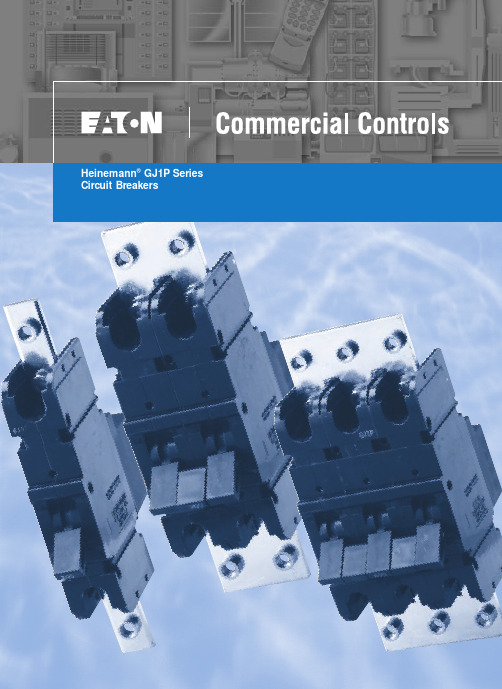
Heinemann®GJ1P Series Circuit BreakersDESCRIPTIONOptional Low-Voltage Shunt for Current MeteringEaton Corporation’s Cutler-Hammer series of Heinemann GJ1P breakers offer high quality circuit protection for DC applications from 100 to 1200 Amperes.Their precisely tailored time delays and ability to interrupt high currents makes them ideally suited for critical applications. On overloads exceeding 1000 – 1400% of rating, there is no intentional time delay and the breaker interrupts currents of as much as 25,000 A at 65V DC.An optional shunt (25 or 50millivolt full scale) permits metering of current. Since the shunt output is low voltage,light-gauge wiring can be used from shunt to meter.Indication may be displayed inpercent, watts, safe/danger or other dial calibrations. In addition, the busbar is available in two versions:Standard Size and Reduced Size. Contact your Eaton Sales Representative for more information.Precision Current Equalization (PCE) Circuit BreakersGJ1P breakers rated 250 to1200 A are built in parallel construction. Conventional parallel pole breakers can experience uneven current distribution because of variations in internalresistances. This condition can result in nuisance tripping since the higher current in one parallel branch has the same effect as an overload on the sensing element in that branch. Proprietary Precision Current Equalization (PCE)circuit breakers, on the other hand, allow for differences in internal resistances byautomatically distributing the current equally through the parallel current sensing elements, minimizing the danger of nuisance tripping.The UL listed series GJ1P (UL489) models are available in a choice of fast, medium or slow response times to accurately match load conditions. They can be ordered in “series trip ”, “mid-trip ” and “switch only ”constructions and are available front- or back-mounted, front- or back-connected, with optional auxiliary switches for signaling.HYDRAULIC-MAGNETIC BENEFITSThe magnetic/hydraulic load-sensing and time delaymechanisms used in GJ1P breakers are insensitive to changes in ambient or enclosure temperature.Therefore, GJ1P circuitbreakers are suited for service conditions encountered in telecommunications,transportation, air conditioning and other outdoor or “heat-loaded ” equipment.SPECIFICATIONSStandard Current Ratings:100, 125, 150, 175, 200, 225,250, 300, 350, 400, 450, 500,600, 700, 800, 900, 1000,1100, 1200 A.Standard Maximum Voltages:160V DC up to 700A65V DC from 701 to 1200A Breakers will be labeled with standard maximum (UL) voltage unless otherwise specified.Special Current Ratings:Any integral rating between 100and 1200 A DC. Consult factory for ordering information and metering shunt restrictions.Interrupting Capacities:UL Listed:10,000 A @ 160V DC 25,000 A @ 65V DC Non-UL:14,000 A @ 160V DC.Operating Temperature Range:-40°C to +85°C.Approximate Weight:1-pole (100-225A) 1.13kg (2.5lbs)2-pole (250-400A) 2.27kg (5lbs)3-pole (450-700A) 3.40kg (7.5lbs)4-pole (701-800A) 4.54kg (10lbs)5-pole (801-1000A) 5.67kg (12.5lbs)6-pole (1001-1200A) 6.80kg (15lbs)Weight may vary based on shunt and busbar.APPROVALSUL Listing:GJ1P breakers are UL listed per UL489. For CSA certification,consult application engineering.Description . . . . . . . . . . . . . .2Specifications . . . . . . . . . . . .2Approvals . . . . . . . . . . . . . . .2Time Delay Characteristics . . .3Dimensions . . . . . . . . . . . .4-5How to Order . . . . . . . . . . .6-7Additional Products. . . . . . . . .8TABLE OF CONTENTS PageHEINEMANN ®CIRCUIT BREAKERSGJ1P Series Circuit Breakers(100-1200 Amperes DC)2Heinemann is a registered trademark of the Eaton Corporation, Commercial Controls Business Unit.100150.01.001.1110100100010,000200300400500600700800900100011001200125C u rv e 1C u rv e 2C u rv e 3Current – Percent of Ampere RatingT r i p T i m e – S e c o n d sDC CURVES100150.01.001.1110100100010,000200300400500600700800900100011001200125Current – Percent of Ampere RatingT r i p T i m e – S e c o n d sINSTANT DELAY DC CURVE PPERCENT OF RATED CURRENT VS. TRIP DELAY AT 25ºCTIME DELAYCHARACTERISTICSTime delay, in all models,is inversely proportional to the magnitude of the overload, adjusting automatically to limit transient power to the load. On overloads exceeding 1,000 –1,400%, the circuit breaker trips without any deliberately imposed delay.Curve 1.Standard time delayis furnished unlessanother optional delay is specified. It is thepreferred characteristic for use where the load is composed of both resistive and inductive components.Curve 2.Medium time delayis for general usein mixed (inductive and resistive) circuits where the breaker rating is matched to the current carrying capacity of the mains.Curve 3.Short time delaypermits a very brief delay period before tripping.Curve P .Non-time delay breakersare available forapplications which cannot tolerate even brief transient overloads.These breakers have no time delay mechanism other than that imposed by the coil self-inductance and the inertia of the mechanism.Tripping specificationsThe time delay curves depict breaker response time vs. percent of rated load with no preloading.The function is plotted at an ambient temperature of 77°F (25°C) with the breaker in a vertical or wall-mounted position.Series GJ1P circuitbreakers will carry 100%of rated load continuously.Both time delay and non-time delay breakers may trip between 101%and 125% of rated load,and must trip at 125%and above.3% (sec)Delay 100%125%200%400%600%800%1000%Delay Max.1no trip 1100150206 1.7.065Delay Min.1no trip 110224 1.1.01.008Delay Max.2no trip 110153.8.28.055Delay Min.2no trip 12 2.5.5.18.01.008Delay Max.3no trip 10.8.19.08.047.038Delay Min.3no trip.44.13.03.015.01.008STANDARD FRONT-CONNECTED CONSTRUCTIONWire Range #6 to 250 MCM74.59(2.938)76.20(3.000)Aux. Terminals, Male Type Molex 02-09-2101, Model 1190-T(See Illustrations for Combinations)Shunt Terminals, Female TypeMolex 02-09-1101, Model 1189-T37.69(1.484)42.84(1.687)0.99 (0.390)71.42(2.812)#10-32 Inserts (4 Places)38.10(1.500)19.05(0.750)19.05(0.750)6.35 ± 0.38(0.250 ± 0.156)6.35 ± 0.38(0.250 ± 0.156)Panel Mounting Hole Distance for #10-32LINELOAD 75.38(2.968)5.53(0.218)59.91(2.359)32.13(1.266)5.53(0.219)“D ” Type Terminals as Shown180.97(7.125)41.27(1.625)4.74(0.188)58.67(2.313)41.27(1.625)41.27(1.625)263.52(10.375)29.36(1.156)7.14(0.281)78.56(3.094)59.13(2.328)28°±5°32°±5°ONOFFSee Optional Terminal ConfigurationWire Range #6to 250 MCM41.27(1.625)36.49(1.437)38.10(1.500)100 – 22 A250 – 400Width dimensions are as follows:100 – 225 38.1 (1.5)250 – 400 A 76.2 (3.0)450 – 700 A 114.3 (4.5)701 – 800A 142.4 (6.0)801 – 1000A 190.5 (7.5)1001 – 1200A228.6 (9.0)28.95(1.141)46.40(1.828)22.22(0.875)Fastener Mounted ThisSide of Bus Plate,Terminals are Front-Connected and Unit is Rear-Mounted.Fastener Mounted This Side of Bus Plate, Terminalsare Back-Connected and Unit is Panel-Mounted.60.32(2.375)7.92(0.312)3/8-16UNC -2B (4 per Unit)38.10(1.500)225.43 (8.875)Center to CenterOptional Terminal ConfigurationsHEINEMANN ®CIRCUIT BREAKERSGJ1P Series Circuit BreakersDIMENSIONSDimensions are given here only as a preliminary guide to specifying. Final engineeringdrawings should be made from the latest Heinemann drawings. Contact Customer Service Center.Tolerance:±0.79 (0.031) except where noted. For metric threads, contact Customer Service Center.DIMENSIONS APPROXIMATE IN MM (INCHES)431.75(1.250) Min.41.65(1.641) Max.19.05(0.750)7.51(0.297)7.51(0.297)7.51(0.297)16.66(0.656)Typ.29.36(1.156)29.36(1.156)48.41(1.906)48.41(1.906)67.46(2.656)67.46(2.656)38.10(1.500)38.10(1.500)38.10(1.500)38.10(1.500)19.05(0.750)19.05(0.750)19.05(0.750)22.23(0.875) Min.321.31(12.65) Max.78.96(3.109)Min. Typ.5.15(0.203)Dia. Typ.C100 – 225 A Ratings 226 – 400 A Ratings401 – 700 150A RatingsBA106.75(4.203)Typ.C LC L C L FRONT MOUNTING PANEL AND SUPPORT BRACKET115.08(4.531)76.98(3.031)38.1(1.500)38.1(1.500)71.42(2.912)5.94(0.234)Ref.5.15(0.203)Typ. Dia.65.02(2.562)59.13(2.328)(3-Pole)3PoleC L C L C L Holes Required When Breaker Is Front-Mounted2Pole1PoleAB C (2-Pole)(1-Pole)38.88(1.531)19.43(0.765)Mounting kits containing clips, brackets and necessary hardware and instructions are available (consult factory).009-18234 100 – 225 A 1.5 (1-pole wide)009-18235 250 – 400 A 3 (2-pole wide)009-18232 450 – 700 A 4.5 (3-pole wide)For 701-1200A devices, contact your Eaton Sales Representative for mounting kit part numbers.See Step (2)See Step (5)BACK MOUNTING CIRCUIT BREAKERBack mounting circuit breaker mounting instructions 1. Position circuit breaker to support brackets.2. Place mounting bracket in recess on front top portion of circuit breaker.3. Install four (4) #10-32 by 3-1/4" long screws through holes in mounting bracket and support structure.4. Install lock washer and nut on each of the screws and tighten.5. Place mounting bracket on front lower portion of circuit breaker.6. Install two (2) #10-32 by 5/8" screws through holes in mounting bracket and support structure.7. Repeat step 4.5DIMENSIONS APPROXIMATE IN MM (INCHES)NOTE: Standard size busbar is shown above. For the reduced size busbar, contact your Eaton Sales Representative for mounting dimensions.Series PrefixGJ1PSwitch (No Coil)Series Trip w/SPDT Aux. SwitchSeries Trip Series Trip and Mid-Trip Series Trip, Mid-Trip and SPST Alarm SwitchTerminal Location Back FrontInternal Circuit Metering ShuntNo Shunts Metering Shunt Metering ShuntB HCodeLocationInternal CircuitCodeDescriptionShuntCode—25mV 50mVP M N0-2-3-98-99-Series Prefix GJ1PTerminal LocationBInternal Circuit3-Metering ShuntPAdd each appropriate Number or Letter …HEINEMANN ®CIRCUIT BREAKERSGJ1P Series Circuit BreakersHOW TO ORDER — Series GJ1PTo determine your Complete Catalog Number , you must start with appropriate Series Prefix and add the appropriate Code Letters and/or Numbers as in the example below:SELECTION TABLE61Multi-pole construction – Consult factory.An auxiliary switch, if supplied, will be located in the right pole space. If the auxiliary switch is supplied in a breaker which has a metering shunt, it will be single-pole single throw (SPST). The single-pole double throw (SPDT) auxiliary switch can be supplied only in a breaker without a metering shunt.2Cannot be used on breaker containing metering shunt.3Only for breakers rated in excess of 250 A. Breakers up to 250 A without meteringshunt are available as standard GJ1 type breakers. Please consult Series GJ catalog.MarketUL-489TerminalsSolderless Connector Bus Bar ConnectionStandard Current Ratings 1AmpereTrip Curve 1123P0 – 1200(Add 0 before amp rating if less than 1000A.Example: 0700)-01-02-03-0PDescriptionCodeDEDUStandardCodeCurveCodeComplete Catalog Number: GJ1PB3-PEDU0700-02Terminal ConfigurationEUS/European ApprovalDUStandard Current Ratings 10700Trip Curves 1-024Add 0 before amp rating if less than 1000. For example: a 700A rating would bedesignated as 0700.The width of the breaker is determined by the current rating:100 – 225 A 1.5” (1-pole wide)250 – 400 A 3” (2-pole wide)450 – 700 A 4.5” (3-pole wide)701 – 800A 6” (4-pole wide)801 – 1000A 7.5” (5-pole wide)1001 – 1200A 9” (6-pole wide)5See page 3 for time delay characteristics and trip curve information.7© 2001 Eaton Corporation All Rights Reserved Printed in USAForm No. BR5401SE0002A / CSS 65322June 2001Commercial ControlsFor the Widest Selection of Circuit Protection, from 0.01 to 1200 Amperes, Look to Eaton.。
ERMAKSAN优玛克光纤激光中文译本

SM2000.3x1.5
YLS2000 10-105 2-2.5
1-2 5 1075±5 100 激光二极管 10 15 10 6 5 4 3000x1500 1500 4 轴(X,Y,Z,U) 3050 1550 150 1.5(2.4 米/秒) 1.5(2.4 米/秒) 1.5(2.4 米/秒)
SM3000.3x1.5
YLS3000 10-105 2-2.5
1-2 5 1075±5 100 激光二极管 20 20 10 8 5 4 3000x1500 1500 4 轴(X,Y,Z,U) 3050 1550 150 1.5(2.4 米/秒) 1.5(2.4 米/秒) 1.5(2.4 米/秒)
W % rad % KHz nm um
l/min mm mm mm mm mm mm KG
mm mm mm G G G
SM1000.3X1.5
YLS1000 10-105 2-2.5
1-2 5 1075±5 50 激光二极管 8
8 4 3 2 2 3000x1500 1500 4 轴(X,Y,Z,U) 3050 1550 150 1.5(2.4 米/秒) 1.5(2.4 米/秒)到,而不是通过在人机界面的复杂操作。 该控制器可以让操作员简单使用机器。 该控制器不受振动,灰尘,潮湿,高温,电磁区,恶劣用法等影响。 活跃的触摸屏和键盘的功能。 快捷按钮能方便使用的特性。 您可以访问所需功能,更快,更容易。 按钮可以被设置为任何快捷键。 速度调整电位器允许您调整轴甚至在切割操作过程中的速度。 开放的接口,通过Ermaksan的工程师,所有软件和控制器开发。 用户期望客户特定的功能设计和补充。 轴运动自动工作交换台,激光等功能的速度设置参数。 功率是按照你的指令控制。
ZXC10 MSCe MGW HLRe的系统结构

中继接入单元
中继接入单元用于实现语音单路的接入 通过DTB/DTEC提供E1和SDTB提供STM-1物理接口
电路交换单元
电路交换单元实现T网交换,处理能力为64K-256K。
由资源子系统(BUSN)中UIMU板和核心电路交换子系统
MGW从功能模块上可以划分为:
IP接入单元 IP包交换单元
中继接入单元
电路交换单元 声码器单元 控制面处理单元 时钟处理单元
IP接入单元
IP接入单元用于实现RTP流的接入和处理
通过IPI可以提供FE和GE物理接口
IP包交换单元
用于实现IP包的交换,这里交换的IP包指的时媒体流的IP包。
HLRe前置机-通用处理模块(CPM)作为介于CDMA网络和 HLRe其他功能模块之间的一个核心模块,主要功能如下:
提供基于TDM和IP的SS7消息接入和处理 提供内存数据库功能 处理HLR MAP消息
接受并处理从操作维护后发送的操作维护指令并返
回相应的操作结果。
前置机CPM的板位
交换单元
交换单元包含了两类单板:
UIM:UIMC
CHUB:实现了不同子系统的以太
网
连接,传递控制流的信息。
时钟单元
ZXC10 HLRe主要功能
移动管理功能
基本呼叫功能
数据业务功能
短信业务功能
补充业务功能
智能网业务功能
ZXC10 HLRe的系统结构
二极管参数
要参数外观封装形式2Package 1Package 21.5A DO-151.5A DO-151.5A DO-151.5A DO-151.5A DO-151.5A DO-151.5A DO-151.5A DO-151.5A DO-152A DO-152A DO-152A DO-152A DO-152A DO-152A DO-152A DO-151.5A DO-151.5A DO-151.5A DO-151.5A DO-151.5A DO-151.5A DO-151.5A DO-151.5A DO-152A DO-152A DO-152A DO-152A DO-152A DO-152A DO-152A DO-152A DO-151.5A DO-151.5A DO-151.5A DO-151.5A DO-151.5A DO-15 1.5A DO-15 1.5A DO-152A DO-15 2A DO-15 2A DO-15 2A DO-15 2A DO-15 2A DO-15 2A DO-15 2A DO-15 2A DO-15 2A DO-15 2A DO-15 2A DO-15 2A DO-15 2A DO-15 2A DO-15 2A DO-15 2A DO-15 2A DO-15DO-15DO-15DO-15DO-15DO-15DO-15DO-15DO-15HVMHVMHVMHVMHVMHVM HVMHVM DO-27 DO-27 DO-27 DO-27 DO-27 DO-27 DO-27 DO-27 DO-27 DO-27 DO-27 DO-27 DO-27 DO-27 DO-27 DO-27 DO-27 DO-27 DO-27 DO-27 DO-27 DO-27 DO-27 DO-27 DO-27 DO-27 DO-27 DO-27 DO-27 DO-27 DO-27 DO-27 DO-27 DO-27 DO-27 DO-27 DO-27 DO-27 DO-27 DO-27 DO-27 DO-27 DO-27DO-27DO-27DO-27DO-27DO-27DO-27DO-27DO-27DO-27DO-27DO-27DO-27DO-27DO-27DO-27DO-27DO-27DO-27DO-27DO-27DO-27DO-27DO-27DO-27DO-27DO-27DO-27 1.5uS DO-350.15A DO-35 0.15A DO-35 0.15A DO-35 0.15A DO-35 0.15A DO-35 0.15A DO-35 0.15A DO-35½W DO-35½W DO-35½W DO-35½W DO-35½W DO-35½W DO-35½W DO-35½W DO-35½W DO-35½W DO-35½W DO-35½W DO-35½W DO-35½W DO-35½W DO-35½W DO-35½W DO-35½W DO-35½W DO-35½W DO-35½W DO-35½W DO-35½W DO-35½W DO-35½W DO-35½W DO-35½W DO-35½W DO-35½W DO-35½W DO-35½W DO-35½W DO-35½W DO-35½W DO-35½W DO-35½W DO-35½W DO-35½W DO-35½W DO-35½W DO-35½W DO-35½W DO-35 250mW DO-35DO-35DO-35DO-35DO-35DO-35DO-35DO-35DO-35DO-35DO-35DO-35DO-35 DO-35 DO-35 DO-35 DO-35 DO-35 DO-35 DO-35 DO-35 DO-35 DO-35 DO-35 DO-35 DO-35 DO-35 DO-35 DO-35 DO-35 DO-35 DO-35 DO-35 DO-35 DO-35 DO-35 DO-35 DO-35 DO-35 DO-35 DO-35 DO-35 DO-35 DO-35 DO-35 DO-35 DO-35 DO-35 DO-35 DO-35 DO-35 DO-35 DO-35 DO-35 DO-35 DO-35 DO-35 DO-35DO-35DO-35DO-35DO-35DO-35DO-35DO-35DO-35DO-35DO-35DO-35DO-35DO-35DO-35DO-35DO-35DO-35DO-35DO-35DO-35DO-35DO-35DO-35DO-35DO-35DO-35DO-35DO-35DO-35Glass SMD DL-35MINI-MELF Glass SMD DL-35MINI-MELF 1W DO-411W DO-411W DO-411W DO-411W DO-411W DO-411W DO-411W DO-411W DO-411W DO-411W DO-411W DO-411W DO-411W DO-411W DO-411W DO-411W DO-411W DO-411W DO-411W DO-411W DO-411W DO-411W DO-411W DO-411W DO-411W DO-411W DO-411W DO-411W DO-411W DO-411W DO-411W DO-411W DO-411W DO-411W DO-411W DO-411W DO-41DO-41 1W DO-41 1W DO-41 1W DO-41 1W DO-41 1W DO-41 V/1W DO-41 V/1W DO-41DO-41DO-41DO-41DO-41DO-41DO-41DO-41DO-41DO-41DO-41DO-41DO-41DO-41DO-41DO-41DO-41DO-41DO-41 DO-41 DO-41 DO-41 DO-41 DO-41 DO-41 DO-41 DO-41 DO-41 DO-41 DO-41 DO-41 DO-41 DO-41 DO-41 DO-41 DO-41 DO-41 DO-41 DO-41DO-41 DO-41 DO-41 DO-41 DO-41 DO-41 DO-41 DO-41DO-41 DO-41 DO-41 DO-41 DO-41 DO-41 DO-41 DO-41 DO-41 DO-41 DO-41DO-41DL-41MELFDL-41MELFDL-41MELFDL-41MELFDL-41MELFDL-41MELFDL-41MELFDL-41MELFDL-41MELFDL-41MELFDL-41MELFDL-41MELFDL-41MELFDL-41MELFDL-41MELFDL-41MELFDL-41MELFDL-41MELFDL-41MELFDL-41MELFDL-41MELFDL-41MELFDL-41MELFDL-41MELFDL-41MELFDL-41MELFDL-41MELFDL-41MELFDL-41MELFDL-41MELFDL-41MELFDL-41MELFDL-41MELFDL-41MELFDL-41MELFDL-41MELFDL-41MELF E-mail: at@DO-201AC SMADO-201AC SMADO-201AC SMADO-213AB SM-1DO-213AB SM-1DO-213AB SM-1DO-213AB SM-1DO-213AB SM-1 DO-213AB SM-1 DO-213AB SM-1 DO-213AB SM-1 DO-213AB SM-1 DO-213AB SM-1 DO-213AB SM-1 DO-213AB SM-1 DO-213AB SM-1 DO-213AB SM-1 DO-213AB SM-1 DO-213AB SM-1 DO-213AB SM-1 DO-213AB SM-1 DO-213AB SM-1 DO-213AB SM-1 DO-213AB SM-1 DO-213AB SM-1 DO-213AB SM-1 DO-213AB SM-1 DO-213AB SM-1 DO-213AB SM-1 DO-213AB SM-1 DO-213AB SM-1 DO-213AB SM-1 DO-213AB SM-1 DO-214AA SMB DO-214AA SMB DO-214AA SMB DO-214AA SMB DO-214AA SMB DO-214AA SMB DO-214AA SMB DO-214AA SMB DO-214AA SMB DO-214AA SMB DO-214AA SMB DO-214AA SMB DO-214AA SMB DO-214AA SMB DO-214AA SMB DO-214AA SMB DO-214AA SMB DO-214AA SMB DO-214AA SMB DO-214AA SMBDO-214AA SMBDO-214AA SMBDO-214AA SMBDO-214AA SMBDO-214AA SMBDO-214AA SMBDO-214AA SMBDO-214AA SMBDO-214AA SMBDO-214AA SMBDO-214AA SMBDO-214AA SMBDO-214AA SMBDO-214AA SMBDO-214AA SMBDO-214AA SMBDO-214AA SMBDO-214AA SMBDO-214AA SMBDO-214AA SMBDO-214AA SMBDO-214AA SMBDO-214AA SMBDO-214AA SMBDO-214AB SMCDO-214AB SMCDO-214AB SMCDO-214AB SMCDO-214AB SMCDO-214AB SMCDO-214AB SMCDO-214AB SMCDO-214AB SMCDO-214AB SMCDO-214AB SMCDO-214AB SMC SCD12DO-214AC SMA SCD13DO-214AC SMA SCD14DO-214AC SMADO-214AC SMADO-214AC SMADO-214AC SMADO-214AC SMADO-214AC SMADO-214AC SMADO-214AC SMADO-214AC SMADO-214AC SMADO-214AC SMADO-214AC SMADO-214AC SMADO-214AC SMADO-214AC SMADO-214AC SMADO-214AC SMADO-214AC SMADO-214AC SMADO-214AC SMADO-214AC SMADO-214AC SMADO-214AC SMADO-214AC SMADO-214AC SMADO-214AC SMADO-214AC SMADO-214AC SMADO-214AC SMADO-214AC SMADO-214AC SMADO-214AC SMADO-214AC SMADO-214AC SMADO-214AC SMADO-214AC SMADO-214AC SMADO-214AC SMADO-214AC SMA201020102010201020102010201020102010:长×宽 2010 mm 20102010SCD SCHOTTKY 2010RRIER RECTIFIERS 20102010201020102010 R-1 R-1 R-1 R-1 R-1 R-1 R-1 R-1 R-1 R-1 R-1 R-1 R-1 R-1 R-1 R-1 R-1 R-1 R-1 R-1 R-1 R-1 R-6 R-6 R-6 R-6 R-6 R-6 R-6 R-6 R-6 R-6 R-6 R-6 R-6 R-6 R-6 R-6 R-6 R-6 R-6 R-6 R-6 R-6 R-6R-6 R-6 R-6 R-6 R-6 R-6M R-6M R-6M R-6M R-6M R-6M R-6M P-600 P-600 P-600 P-600 P-600 P-600 P-600 P-600 P-600 P-600 P-600 P-600 P-600 P-600 A-405 A-405 A-405 A-405 A-405 A-405 A-405 A-405 A-405 A-405 A-405 A-405 A-405 A-405 A-405 A-405 A-405 A-405 A-405 A-405TO-220ABTO-220ABTO-220ABTO-220ABTO-220ABTO-220ABTO-220ABTO-220ABTO-220ABTO-220ABTO-220ABTO-220ABTO-220ABTO-220ABTO-220ABTO-220ABTO-220ABTO-220ABTO-220ABTO-220ABTO-220ABTO-220ABTO-3PTO-3PTO-3PTO-3PTO-3PTO-3PTO-3PTO-3PTO-3PSOT-235V SOT-230V SOT-230V SOT-230V SOT-230V SOT-230V SOT-23 50V SOT-23 100V SOT-23 100V SOT-23 100V SOT-23 120V SOT-23 180V SOT-23 250V SOT-23350mW/100V SOT-23100V SOT-23100V SOT-23100V SOT-23100V SOT-23100V SOT-23100V SOT-23100V SOT-23100V SOT-23100V SOT-23100V SOT-230V SOT-235V SOT-235V SOT-230V SOT-23SOT-23SOT-23SOT-23SOT-23SOT-23SOT-23SOT-23SOT-23SOT-23SOT-23SOT-23SOT-23SOT-23SOT-23SOT-23SOT-23SOT-23SOT-23SOT-23SOT-23SOT-23SOT-23SOT-23SOT-23SOT-23SOT-23SOT-23SOT-23SOT-23SOT-23SOT-23SOT-23SOT-23SOT-23SOT-23SOT-23SOT-23SOT-23 5V SOT-23 5V SOT-23 5V SOT-23 5V SOT-23 5V SOT-23 5V SOT-23 5V SOT-23 5V SOT-23 5V SOT-23 5V SOT-23 5V SOT-23 5V SOT-23 5V SOT-23 5V SOT-23 5V SOT-23 5V SOT-23 5V SOT-23 5V SOT-23 5V SOT-23 5V SOT-23 5V SOT-23 5V SOT-23 5V SOT-23 5V SOT-23 5V SOT-23 5V SOT-23 5V SOT-23 5V SOT-23 5V SOT-23 5V SOT-23 5V SOT-23 5V SOT-23 5V SOT-23 5V SOT-23 5V SOT-23 5V SOT-23 250V SOD-123 100V SOD-123 100V SOD-123 50V SOD-123 120V SOD-123410mW/180V SOD-12375V SOD-123100V SOD-123SOD-323SOD-323SOD-323SOD-323SOD-323SOD-323SOD-323SOD-323SOD-323SOD-323SOD-323SOD-323SOD-323SOD-323SOD-323SOD-323SOD-323I ZT: 20mA SOT-32320mA SOT-32320mA SOT-32320mA SOT-32320mA SOT-32320mA SOT-32320mA SOT-32320mA SOT-32320mA SOT-32320mA SOT-32320mA SOT-32320mA SOT-32320mA SOT-32320mA SOT-32320mA SOT-323 20mA SOT-323 20mA SOT-323 20mA SOT-323 20mA SOT-323 20mA SOT-323 20mA SOT-323 20mA SOT-323 9.5mA SOT-323 9mA SOT-323 8.5mA SOT-323 7.8mA SOT-323 7.4mA SOT-323 7mA SOT-323 6.6mA SOT-323 6.2mA SOT-323 5.6mA SOT-323 5.2mA SOT-323 5mA SOT-323 4.6mA SOT-323 4.5mA SOT-323 4.2mA SOT-323 3.8mA SOT-323 3.4mA SOT-323 3.2mA SOT-323 3mA SOT-323 2.7mA SOT-323 2.5mA SOT-323½W DL-35MINI-MELF/Glas s SMD½W DL-35MINI-MELF/Glas s SMD½W LL-34SOD-80C/Mini-Melf½W LL-34SOD-80C/Mini-Melf½W LL-34SOD-80C/Mini-Melf½W LL-34SOD-80C/Mini-Melf½W LL-34SOD-80C/Mini-Melf½W LL-3480C/Mini-Melf½W LL-34SOD-80C/Mini-Melf½W LL-34SOD-80C/Mini-Melf½W LL-34SOD-80C/Mini-Melf½W LL-34SOD-80C/Mini-Melf½W LL-34SOD-80C/Mini-Melf½W LL-34SOD-80C/Mini-Melf½W LL-34SOD-80C/Mini-Melf½W LL-34SOD-80C/Mini-Melf½W LL-34SOD-80C/Mini-Melf½W LL-34SOD-80C/Mini-Melf½W LL-34SOD-80C/Mini-Melf½W LL-34SOD-80C/Mini-Melf½W LL-34SOD-80C/Mini-Melf½W LL-34SOD-80C/Mini-Melf½W LL-34SOD-80C/Mini-Melf½W LL-34SOD-80C/Mini-Melf½W LL-3480C/Mini-Melf½W LL-34SOD-80C/Mini-Melf½W LL-34SOD-80C/Mini-Melf½W LL-34SOD-80C/Mini-Melf½W LL-34SOD-80C/Mini-Melf½W LL-34SOD-80C/Mini-Melf½W LL-34SOD-80C/Mini-Melf½W LL-34SOD-80C/Mini-Melf½W LL-34SOD-80C/Mini-Melf½W LL-34SOD-80C/Mini-Melf½W LL-34SOD-80C/Mini-Melf½W LL-34SOD-80C/Mini-Melf½W LL-34SOD-80C/Mini-Melf½W LL-34SOD-80C/Mini-Melf½W LL-34SOD-80C/Mini-Melf½W LL-34SOD-80C/Mini-Melf½W LL-34SOD-80C/Mini-Melf。
- 1、下载文档前请自行甄别文档内容的完整性,平台不提供额外的编辑、内容补充、找答案等附加服务。
- 2、"仅部分预览"的文档,不可在线预览部分如存在完整性等问题,可反馈申请退款(可完整预览的文档不适用该条件!)。
- 3、如文档侵犯您的权益,请联系客服反馈,我们会尽快为您处理(人工客服工作时间:9:00-18:30)。
MC10H107Triple 2−Input Exclusive OR/ Exclusive NOR GateDescriptionThe MC10H107 is a triple 2−input exclusive OR/NOR gate. This MECL 10H™ part is a functional/pinout duplication of the standard MECL 10K™ family part, with 100% improvement in propagation delay, and no increase in power−supply current.Features•Propagation Delay, 1.0 ns Typical•Power Dissipation 35 mW/Gate Typical (same as MECL 10K)•Improved Noise Margin 150 mV (Over Operating V oltage and Temperature Range)•V oltage Compensated•MECL 10K Compatible•Pb−Free Packages are Available**For additional information on our Pb−Free strategy and soldering details, please download the ON Semiconductor Soldering and Mounting Techniques Reference Manual, SOLDERRM/D.See detailed ordering and shipping information in the package dimensions section on page 3 of this data sheet.ORDERING INFORMATIONFigure 1. Logic Diagram Figure 2. Pin AssignmentV CC1A outA out A in A in *NCB in V EEV CC2C in C in C out C out B out B out B in16151413121110912345678V CC1 = Pin 1V CC2 = Pin 16V EE = Pin 8151314941210113275*NC = No ConnectionPin assignment is for Dual −in −Line Package.Table 1. MAXIMUM RATINGSSymbol CharacteristicRating Unit V EE Power Supply (V CC = 0)−8.0 to 0Vdc V I Input Voltage (V CC = 0)0 to V EE Vdc I out Output CurrentContinuousSurge50100mA T A Operating Temperature Range 0 to +75°C T stgStorage Temperature RangePlastic Ceramic −55 to +150−55 to +165°C °CMaximum ratings are those values beyond which device damage can occur. Maximum ratings applied to the device are individual stress limit values (not normal operating conditions) and are not valid simultaneously. If these limits are exceeded, device functional operation is not implied,damage may occur and reliability may be affected.Table 2. ELECTRICAL CHARACTERISTICS (V EE = −5.2 V ±5%) (Note 1)0°25°75°Symbol CharacteristicMin Max Min Max Min Max Unit I E Power Supply Current −31−28−31mA I inH Input Current High −425−265−265m A I inL Input Current Low 0.5−0.5−0.3−m A V OH High Output Voltage −1.02−0.84−0.98−0.81−0.92−0.735Vdc V OL Low Output Voltage −1.95−1.63−1.95−1.63−1.95−1.60Vdc V IH High Input Voltage −1.17−0.84−1.13−0.81−1.07−0.735Vdc V ILLow Input Voltage−1.95−1.48−1.95−1.48−1.95−1.45Vdc1.Each MECL 10H series circuit has been designed to meet the dc specifications shown in the test table, after thermal equilibrium has been established. The circuit is in a test socket or mounted on a printed circuit board and transverse air flow greater than 500 linear fpm is maintained. Outputs are terminated through a 50 W resistor to −2.0 V.Table 3. AC CHARACTERISTICS0°25°75°Symbol Characteristic Min Max Min Max Min Max Unitt pd Propagation Delay0.4 1.50.4 1.60.4 1.7nst r Rise Time0.5 1.50.5 1.60.5 1.7nst f Fall Time0.5 1.50.5 1.60.5 1.7ns NOTE:Device will meet the specifications after thermal equilibrium has been established when mounted in a test socket or printed circuit board with maintained transverse airflow greater than 500 lfpm. Electrical parameters are guaranteed only over the declaredoperating temperature range. Functional operation of the device exceeding these conditions is not implied. Device specification limit values are applied individually under normal operating conditions and not valid simultaneously.ORDERING INFORMATIONDevice Package Shipping†MC10H107FN PLLC−2046 Units / RailMC10H107FNG PLLC−20(Pb−Free)46 Units / RailMC10H107FNR2PLLC−20500 / Tape & ReelMC10H107FNR2G PLLC−20(Pb−Free)500 / Tape & ReelMC10H107L CDIP−1625 Unit / RailMC10H107M SOEIAJ−1650 Unit / RailMC10H107MG SOEIAJ−16(Pb−Free)50 Unit / RailMC10H107MEL SOEIAJ−162000 / Tape & ReelMC10H107MELG SOEIAJ−16(Pb−Free)2000 / Tape & ReelMC10H107P PDIP−1625 Unit / RailMC10H107PG PDIP−16(Pb−Free)25 Unit / Rail†For information on tape and reel specifications, including part orientation and tape sizes, please refer to our Tape and Reel Packaging Specifications Brochure, BRD8011/D.PACKAGE DIMENSIONSSL−MS 0.010 (0.250) NST 20 LEAD PLLC CASE 775−02ISSUE ENOTES:1.DIMENSIONS AND TOLERANCING PER ANSI Y14.5M,1982.2.DIMENSIONS IN INCHES.3.DATUMS −L −, −M −, AND −N − DETERMINED WHERE TOP OF LEAD SHOULDER EXITS PLASTIC BODY AT MOLD PARTING LINE.4.DIMENSION G1, TRUE POSITION TO BE MEASURED AT DATUM −T −, SEATING PLANE.5.DIMENSIONS R AND U DO NOT INCLUDE MOLD FLASH.ALLOWABLE MOLD FLASH IS 0.010 (0.250) PER SIDE.6.DIMENSIONS IN THE PACKAGE TOP MAY BE SMALLER THAN THE PACKAGE BOTTOM BY UP TO 0.012 (0.300).DIMENSIONS R AND U ARE DETERMINED AT THE OUTERMOST EXTREMES OF THE PLASTIC BODY EXCLUSIVE OF MOLD FLASH, TIE BAR BURRS, GATE BURRS AND INTERLEAD FLASH, BUT INCLUDING ANY MISMATCH BETWEEN THE TOP AND BOTTOM OF THE PLASTIC BODY .7.DIMENSION H DOES NOT INCLUDE DAMBAR PROTRUSION OR INTRUSION. THE DAMBARPROTRUSION(S) SHALL NOT CAUSE THE H DIMENSION TO BE GREATER THAN 0.037 (0.940). THE DAMBARINTRUSION(S) SHALL NOT CAUSE THE H DIMENSION TO BE SMALLER THAN 0.025 (0.635).DIM MIN MAX MIN MAX MILLIMETERSINCHES A 0.3850.3959.7810.03B 0.3850.3959.7810.03C 0.1650.180 4.20 4.57E 0.0900.110 2.29 2.79F 0.0130.0190.330.48G 0.050 BSC 1.27 BSC H 0.0260.0320.660.81J 0.020−−−0.51−−−K 0.025−−−0.64−−−R 0.3500.3568.899.04U 0.3500.3568.899.04V 0.0420.048 1.07 1.21W 0.0420.048 1.07 1.21X 0.0420.056 1.07 1.42Y −−−0.020−−−0.50Z 2 10 2 10 G10.3100.3307.888.38K10.040−−− 1.02−−−____PACKAGE DIMENSIONSSOEIAJ −16CASE 966−01ISSUE ANOTES:1.DIMENSIONING AND TOLERANCING PER ANSI Y14.5M, 1982.CDIP −16L SUFFIXCERAMIC DIP PACKAGECASE 620A −01NOTES:1.DIMENSIONING AND TOLERANCING PER ASME Y14.5M, 1994.2.CONTROLLING DIMENSION: INCH.3.DIMENSION L TO CENTER OF LEAD WHEN FORMED PARALLEL.4.DIMENSION F MAY NARROW TO 0.76 (0.030)WHERE THE LEAD ENTERS THE CERAMIC BODY.5THIS DRAWING REPLACES OBSOLETE CASE OUTLINE 620−10.AM0.25 (0.010)T DIM MIN MAX MIN MAX MILLIMETERSINCHES A 0.7500.78519.0519.93B 0.2400.295 6.107.49C −−−0.200−−− 5.08D 0.0150.0200.390.50E 0.050 BSC 1.27 BSC F 0.0550.065 1.40 1.65G 0.100 BSC 2.54 BSC H 0.0080.0150.210.38K 0.1250.170 3.18 4.31L 0.300 BSC 7.62 BSC M 0 15 0 15 N0.0200.0400.51 1.01____PACKAGE DIMENSIONSNOTES:1.DIMENSIONING AND TOLERANCING PER ANSI Y14.5M, 1982.2.CONTROLLING DIMENSION: INCH.3.DIMENSION L TO CENTER OF LEADS WHEN FORMED PARALLEL.4.DIMENSION B DOES NOT INCLUDE MOLD FLASH.5.ROUNDED CORNERS OPTIONAL.MDIM MIN MAX MIN MAX MILLIMETERSINCHES A 0.7400.77018.8019.55B 0.2500.270 6.35 6.85C 0.1450.175 3.69 4.44D 0.0150.0210.390.53F 0.0400.70 1.02 1.77G 0.100 BSC 2.54 BSC H 0.050 BSC 1.27 BSC J 0.0080.0150.210.38K 0.1100.130 2.80 3.30L 0.2950.3057.507.74M 0 10 0 10 S0.0200.0400.51 1.01____PDIP −16P SUFFIXPLASTIC DIP PACKAGEON Semiconductor and are registered trademarks of Semiconductor Components Industries, LLC (SCILLC). SCILLC reserves the right to make changes without further notice to any products herein. SCILLC makes no warranty, representation or guarantee regarding the suitability of its products for any particular purpose, nor does SCILLC assume any liability arising out of the application or use of any product or circuit, and specifically disclaims any and all liability, including without limitation special, consequential or incidental damages.“Typical” parameters which may be provided in SCILLC data sheets and/or specifications can and do vary in different applications and actual performance may vary over time. All operating parameters, including “Typicals” must be validated for each customer application by customer’s technical experts. SCILLC does not convey any license under its patent rights nor the rights of others. SCILLC products are not designed, intended, or authorized for use as components in systems intended for surgical implant into the body, or other applications intended to support or sustain life, or for any other application in which the failure of the SCILLC product could create a situation where personal injury or death may occur. Should Buyer purchase or use SCILLC products for any such unintended or unauthorized application, Buyer shall indemnify and hold SCILLC and its officers, employees, subsidiaries, affiliates,and distributors harmless against all claims, costs, damages, and expenses, and reasonable attorney fees arising out of, directly or indirectly, any claim of personal injury or death associated with such unintended or unauthorized use, even if such claim alleges that SCILLC was negligent regarding the design or manufacture of the part. SCILLC is an Equal Opportunity/Affirmative Action Employer. This literature is subject to all applicable copyright laws and is not for resale in any manner.PUBLICATION ORDERING INFORMATIONMECL 10H and MECL 10K are trademarks of Motorola, Inc.。