HT1602中文资料
1602液晶资料

1602液晶资料一、介绍1602液晶是一种常见的字符型液晶显示器,可以显示16列2行共32个字符。
它采用了液晶显示技术,使得显示效果更加清晰、稳定。
1602液晶广泛应用于各种嵌入式系统、电子设备以及 DIY 项目中。
本文将介绍1602液晶的基本原理、接口定义、使用方法以及常见应用场景。
二、基本原理1602液晶的基本原理是利用液晶分子的取向和电场作用的变化来改变光的透过与反射。
它由1602个独立的像素(80列×2行)组成,每个像素有一个电极对和一个液晶分子,液晶分子的取向可以通过施加电场来改变。
1602液晶由背光源、液晶面板、驱动电路和控制电路等组成,背光源提供背光使得字符能够显示在显示器上。
三、接口定义1602液晶显示器通常通过并行接口与主控单元进行通信,下面是1602液晶的常用接口定义:•DB0-DB7:并行数据接口,用于传输数据与指令。
•RS:指令/数据选择信号,用于控制将数据写入显示器还是发送给控制器.•R/W:读/写选择信号,用于选择进行读操作或写操作。
•E:使能信号,用于控制读写操作的时序。
•VSS:地线,用于提供电流的回路。
•VDD:电源正极,提供1602液晶的工作电源。
•V0:液晶偏置电压,通过该电压设置液晶显示的对比度。
•A:背光灯电源正极,提供背光灯的工作电源。
•K:背光灯电源负极,提供背光灯工作电流的回路。
四、使用方法使用1602液晶显示器需要以下步骤:1.连接电路:根据接口定义,将1602液晶与主控单元进行正确的连接。
注意接线的准确性,以免引起电路故障。
2.初始化:在使用1602液晶之前,需要对其进行初始化。
初始化的过程一般包括设置显示模式、清屏以及设置光标位置等。
3.写入数据:通过并行接口将想要显示的数据或指令传输给1602液晶,可以显示各种字符、数字、符号等。
4.控制显示:通过指令设置1602液晶的显示方式,包括光标显示、光标闪烁、显示开关等。
5.清屏:清除1602液晶的显示内容,可以使用指令或者写入空格字符来实现。
HT1621B-1

深圳明和科技有限公司
管脚配置
Tel:0755-82536500 Fax:82536214
底板插口配置
芯片大小 127 129(mil)2 -2-
深圳明和科技有限公司
Tel:0755-82536500 Fax:82536214
底板插口坐标
底板插口描述
插口号 插口名
I/O
1 /CS
I
2 /RD
I
3 /WR
I
4 DATA
I/O
5 VSS
I
7 OSCI
I
6 OSCO
O
8 VLCD
I
9 VDD
I
10 /IRQ
O
11 12 BZ,/BZ
O
13 16 COM0~COM3 O
17 48 SEG0~SEG31 O
功能描述
片选输入 接一上拉电阻 当/CS 为高电平 读写 HT1621 的数据和命令无效 串行接口电路复位 当/CS 为低电平和作为输入时 读写 HT1621 的数据和命令有效 READ 脉冲输入 接一上拉电阻 在/RD 信号的下降沿 HT1621 内存的数据被读到 DATA 线上 主控制器可以在下一个上升沿时锁存这 些数据
最大 值 5.2 300 600 120 240 200 400 5 10 0.6 1.0 3.0 5.0
150 100
单位
V
A A A A A A A A
V V V V mA mA mA mA
A
A A A A A A
A
K K
-4-
深圳明和科技有限公司
Tel:0755-82536500 Fax:82536214
WRITE 脉冲输入 接一上拉电阻 在 /WR 信 号 的 上 升 沿 DATA 线 上 的 数 据 写 到
TH160里氏硬度计使用说明书
TH160里氏硬度计使用说明书TH160里氏硬度计产品特点1.主显示界面与HLN-11A里氏硬度计相似,令老用户倍感亲切。
2.打印机与主机集成一体设计。
3.大屏幕点阵液晶,采用320×200图形点阵液晶显示器,字体及图形美观,信息丰富、清晰。
4.内置锂离子充电电池及充电控制电路,无记忆效应,充电方便,寿命长。
5.采用热敏式打印机,工作安静,可打印任意份数的测试结果,满足现场的需要,免去了更换色带的麻烦。
6.全中文显示,菜单式操作,按键少,操作简单方便。
7.带有RS232接口,多种通讯方式适应不同用户的个性需求。
8.具有自动识别常用冲击方向功能(除G型冲击装置外)。
9.一台主机可配备7种不同冲击装置使用,更换时不需重新校准,自动识别冲击装置类型。
10.大容量存储器,可存储240~1000组(冲击次数32~1)单次测量值、平均值、测量日期、冲击方向、次数、材料、硬度制等信息。
11.可预先设置硬度值上、下限,超出范围自动报警,方便用户批量测试的需要。
12.有背光显示,方便用户野外使用。
13.主显示界面增加了日期、时间、存储器信息、电池信息、电子柱、超差提示、冲击装置类型、操作提示等内容,更加方便实用。
14.所有显示界面均有操作提示,便于操作。
15.液晶上有充电过程指示,操作者可随时了解充电程度,带有充电指示灯,是否处于充电状态一目了然。
16.具有示值软校准功能。
17.增加了“锻钢(Steel)”材料,当用D型冲击装置测试“锻钢”试样时,可直接读取HS值,省去了人工查表的麻烦。
18.根据用户的要求,可配备微机软件,功能更加强大,满足质量保证活动和管理的更高要求。
1.2TH160里氏硬度计主要用途及适用范围1.2.1TH160里氏硬度计主要用途1.已安装的机械或永久性组装部件。
2.模具型腔。
3.重型工件。
4.压力容器、汽轮发电机组及其设备的失效分析。
5.试验空间很狭小的工件。
6.轴承及其它零件。
1602的中文资料
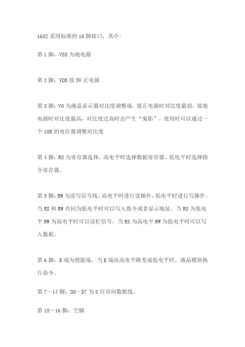
1602采用标准的16脚接口,其中:第1脚:VSS为地电源第2脚:VDD接5V正电源第3脚:V0为液晶显示器对比度调整端,接正电源时对比度最弱,接地电源时对比度最高,对比度过高时会产生“鬼影”,使用时可以通过一个10K的电位器调整对比度第4脚:RS为寄存器选择,高电平时选择数据寄存器、低电平时选择指令寄存器。
第5脚:RW为读写信号线,高电平时进行读操作,低电平时进行写操作。
当RS和RW共同为低电平时可以写入指令或者显示地址,当RS为低电平RW为高电平时可以读忙信号,当RS为高电平RW为低电平时可以写入数据。
第6脚:E端为使能端,当E端由高电平跳变成低电平时,液晶模块执行命令。
第7~14脚:D0~D7为8位双向数据线。
第15~16脚:空脚1602液晶模块内部的字符发生存储器(CGROM)已经存储了160个不同的点阵字符图形,如表1所示,这些字符有:阿拉伯数字、英文字母的大小写、常用的符号、和日文假名等,每一个字符都有一个固定的代码,比如大写的英文字母“A”的代码是01000001B(41H),显示时模块把地址41H中的点阵字符图形显示出来,我们就能看到字母“A”1602液晶模块内部的控制器共有11条控制指令,如表2所示,它的读写操作、屏幕和光标的操作都是通过指令编程来实现的。
(说明:1为高电平、0为低电平)指令1:清显示,指令码01H,光标复位到地址00H位置指令2:光标复位,光标返回到地址00H指令3:光标和显示模式设置 I/D:光标移动方向,高电平右移,低电平左移 S:屏幕上所有文字是否左移或者右移。
高电平表示有效,低电平则无效指令4:显示开关控制。
D:控制整体显示的开与关,高电平表示开显示,低电平表示关显示 C:控制光标的开与关,高电平表示有光标,低电平表示无光标 B:控制光标是否闪烁,高电平闪烁,低电平不闪烁指令5:光标或显示移位 S/C:高电平时移动显示的文字,低电平时移动光标指令6:功能设置命令 DL:高电平时为4位总线,低电平时为8位总线N:低电平时为单行显示,高电平时双行显示 F: 低电平时显示5x7的点阵字符,高电平时显示5x10的点阵字符指令7:字符发生器RAM地址设置指令8:DDRAM地址设置指令9:读忙信号和光标地址 BF:为忙标志位,高电平表示忙,此时模块不能接收命令或者数据,如果为低电平表示不忙。
字符液晶显示原理实例详解

1602详细资料和实例1602字符液晶在实际的产品中运用的也比较多了,前几天留意了一下,发现宿舍门前的自动售水机就是采用的1602液晶进行显示的。
而且对于单片机的学习而言,掌握1602的用法是每一个学习者必然要经历的过程。
在此,我将使用1602过程中遇到的问题以及感受记录下来,希望能够给初学者带来一点指导,少走一点弯路。
所谓1602是指显示的内容为16*2,即可以显示两行,每行16个字符。
目前市面上字符液晶绝大多数是基于HD44780液晶芯片的,控制原理是完全相同的,因此基于HD44780写的控制程序可以很方便地应用于市面上大部分的字符型液晶。
1602液晶的正面(绿色背光,黑色字体)1602液晶背面(绿色背光,黑色字体)另一种1602液晶模块,显示屏是蓝色背光白色字体字符型LCD1602通常有14条引脚线或16条引脚线的LCD,多出来的2条线是背光电源线VCC(15脚)和地线GND(16脚),其控制原理与14脚的LCD完全一样,引脚定义如下表所示:HD44780内置了DDRAM、CGROM和CGRAM。
DDRAM就是显示数据RAM,用来寄存待显示的字符代码。
共80个字节,其地址和屏幕的对应关系如下表:也就是说想要在LCD1602屏幕的第一行第一列显示一个"A"字,就要向DDRAM的00H地址写入“A”字的代码(指A的字模代码,0x20~0x7F为标准的ASCII码,通过这个代码,在CGROM中查找到相应的字符显示)就行了。
但具体的写入是要按LCD模块的指令格式来进行的,后面我会说到的。
那么一行可有40个地址呀?是的,在1602中我们就用前16个就行了。
第二行也一样用前16个地址。
对应如下:DDRAM地址与显示位置的对应关系。
(事实上我们往DDRAM里的00H地址处送一个数据,譬如0x31(数字1的代码,见字模关系对照表)并不能显示1出来。
这是一个令初学者很容易出错的地方,原因就是如果你要想在DDRAM的00H地址处显示数据,则必须将00H加上80H,即80H,若要在DDRAM的01H处显示数据,则必须将01H加上80H即81H。
1602技术资料
1.Mechanical Specification2Mechanical Diagram3. Interface Pin Connections4. Block Diagram5. Absolute Maximum Rating6. Electrical Characteristics7. Optical Characteristics8. Optical Definitions9. Display Address10. Interface to MPU10.1 Interface to Z-80 CPU10.2 Interface to MC6800 CPU CONTENTSPAGE22223333344410.3 Interface to 4-bit CPU ( HMCS43C )10.4 Interface to HD6805 MP11. Timing Control11.1 Write and Read Operation11.2 Busy flag check timing12. Initialization of LCM13. Instruction Set14. User Font Patterns15. Software Example15.1 8-bit operation ( 8 bits 2 lines )15.2 4-bit operation ( 4 bits 2 lines )16. Reliability Condition17. Function Test & Inspection Criteria18 Character Generator ROM MapPAGE 1 (CTM1602-04A Serial)4444456677881071. Mechanical Specification3. Interface Pin Connections4. Black Diagram5. Absolute Maximum Ratings6. Electrical Characteristics7. Optical Characteristics8. Optical DefinitionsResponse Time9. Display AddressContrast Ration ViewAnglePAGE 3 (CTM1602-04A Serial)10. Interface to MPU10.1 Interface to Z-80 CPU10.3 Interface to 4-bit CPU ( HMCS43C ) 11. Timing Control11.1 Write and Read OperationWrite Operation10.2 Interface to MC6800 CPU10.4 Interface to HD6805 MPRead Operation11.2 Busy flag check timingPAGE 4 (CTM1602-04A Serial)12. Initialization of LCMThe LCM automatically initializes ( reset ) when power is turned on using the internal reset circuit. If the power supply conditions for correctly operating of the internal reset circuit are not met, initialization by instruction is required. Use the procedure is next page for initialization. Internal Power Supply reset4.5VVcc0.2Vtoff→← trcc←-----→(Note 1) 10 ms ≧ trcc ≧ 0.1 ms , toff ≧ 1 ms.(Note 2) toff stipulates the time of power OFF for momentary power supply dip or when power supply cycles ON and OFF.1) 8 Bit Interface2) 4 Bit Interface Busy flag is checked after instructions are completed. If busy flay isn ‘t checked, the waiting time between instructions should be longer than execution time of these instructions.PAGE 5 (CTM1602-04A Serial)13. Instruction Set14. User Font Patterns ( CG RAM Character )PAGE 6 (CTM1602-04A Serial)15. Software Example15.1 8-bit operation ( 8 bits 2 lines )15.2 4-bit operation ( 4-bit, 1 line )PAGE 7 (CTM1602-04A Serial)16. Reliability Condition*Wide temp. version may not available for some products, Please consult our sales engineer or respresentative.17. Functional Test & Inspection Criteria17.1 Sample planSample plan according to MIL-STD-105E level 2, and acceptance/rejection criteria is.Base on : Major defect : AQL 0.65 Minor defect : AQL 1.517.2 Inspection conditionViewing distance for cosmetic inspection is 30cm with bare eyes, and under an environment of 800 lus (20W) light intensity. All direction for inspecting the sample should be within 45°against perpendicular line.17.3 Definition of Inspection Zone in LCDCA BZone A : Character / Digit areaZone B : Viewing area except Zone A ( Zone A + Zone B = minimum Viewing area )Zone C : Outside viewing area ( invisible area after assembly in customer’s product )Note : As a general rule, visual defects in Zone C are permissible, when it is no trouble for quality and assembly of customer’s product.17.4 Major DefectAll functional defects such as open ( or missing segment ), short, contrast differential, excesspower consumption, smearing, leakage, etc. and overall outline dimension beyond the drawing.Are classified as major defects.PAGE 8 (CTM1602-04A Serial)17.5 Minor DefectPAGE 9 (CTM1602-04A Serial)18. Character Generator ROM Map0000 0010 0011 0100 0101 0110 0111 1010 1011 1100 1101 1110 1111PAGE 10 (CTM1602-04A Serial)。
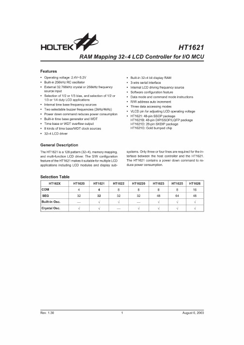
HT16C21规格书
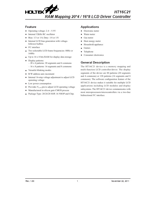
Rev. 1.001November 22, 2011HT16C21RAM Mapping 20*4 / 16*8 LCD Driver ControllerFeature●Operating voltage: 2.4 ~ 5.5V ●Internal 32kHz RC oscillator●Bias: 1/3 or 1/4; Duty: 1/4 or 1/8●Internal LCD bias generation with voltage-follower buffers ●I 2C interface●Two selectable LCD frame frequencies: 80Hz or 160Hz●Up to 16 x 8 bits RAM for display data storage ●Display patterns:–20 x 4 patterns: 20 segments and 4 commons –16 x 8 patterns: 16 segments and 8 commons ●Versatile blinking modes ●R/W address auto increment●Internal 16-step voltage adjustment to adjust LCD operating voltage ●Low power consumption●Provides V LCD pin to adjust LCD operating voltage ●Manufactured in silicon gate CMOS process●Package Type: 20/24/28 SOP, 16 NSOP and Chip.Applications●Electronic meter ●Water meter ●Gas meter●Heat energy meter ●Household appliance ●Games●Telephone●Consumer electronicsGeneral DescriptionThe HT16C21 device is a memory mapping and multi-function LCD controller/driver. The display segments of the device are 80 patterns (20 segments and 4 commons) or 128 patterns (16 segments and 8 commons). The software configuration feature of the HT16C21 device makes it suitable for multiple LCD applications including LCD modules and display subsystems. The HT16C21 device communicates with most microprocessors/microcontrollers via a two-line bidirectional I 2C interface.Rev. 1.002November 22, 2011Block DiagramCOM0COM3SEG4VSS SDA SCLCOM4/SEG0COM7/SEG3SEG19Rev. 1.003November 22, 2011Pin AssignmentVDD SDASCL VSS COM0COM1COM2COM3COM4/SEG0COM5/SEG1COM6/SEG2COM7/SEG3SEG19/VLCD SEG18SEG15SEG14SEG13SEG12SEG11SEG10SEG7SEG6SEG5SEG4VDD SDA SCL VSS COM0COM1COM2COM3SEG19/VLCD SEG14SEG13SEG12COM7/SEG3COM6/SEG2COM5/SEG1COM4/SEG0VDD SDASCL VSS COM0COM1COM2COM3COM4/SEG0COM5/SEG1SEG19/VLCD SEG18SEG13SEG12SEG11SEG10SEG5SEG4COM7/SEG3COM6/SEG2VDD SDASCL VSS COM0COM1COM2COM3COM4/SEG0COM5/SEG1COM6/SEG2COM7/SEG3SEG4SEG5SEG19/VLCD SEG18SEG17SEG16SEG15SEG14SEG13SEG12SEG11SEG10SEG9SEG8SEG7SEG6HT16C2124 SOP-A HT16C2128 SOP-AHT16C2116 NSOP-A HT16C2120 SOP-ARev. 1.004November 22, 2011Pad assignment for COBSEG10SEG9SEG8SEG7SEG6SEG5SEG4COM7/SEG3COM6/SEG2COM5/SEG1COM4/SEG0COM0COM1COM2COM3SEG14SEG13SEG12SEG11V S SS C LS D AV D D V C C A 2V L C DS E G 19S E G 18S E G 17S E G 16S E G 15Chip size: 1200 x 1846μm 2Note: 1. The IC substrate should be connected to V SS in the PCB layout artwork.2. VDD (Pad29) and VCCA2 (Pad28) must be bonded together.3. VLCD (Pad27) and SEG19 (Pad26) must be bonded together.Pad Coordinates for COBPin DescriptionApproximate Internal ConnectionsAbsolute Maximum RatingsSupply voltage ......................................................................................................................V SS−0.3V to V SS+6.5V Input voltage ........................................................................................................................V SS−0.3V to V DD+0.3V Storage temperature .......................................................................................................................-55°C to +150°C Operating temperature .....................................................................................................................-40°C to +85°C Note: These are stress ratings only. Stresses exceeding the range specified under "Absolute Maximum Ratings"may cause substantial damage to the device. Functional operation of this device at other conditions beyond those listed in the specification is not implied and prolonged exposure to extreme conditions may affect device reliability.Rev. 1.005November 22, 2011Rev. 1.006November 22, 2011Note: 1. If the conditions of Power on Reset timing are not satisfied during the power ON/OFF sequence, the internal Power on Reset (POR) circuit will not operate normally.2. If the V DD voltage drops below the minimum voltage of operating voltage spec. during operating, thePower on Reset timing conditions must also be satisfied. That is, the V DD voltage must drop to 0V and remain at 0V for 20ms (min.) before rising to the normal operating voltage.A.C. Characteristics – I2C InterfaceRev. 1.007November 22, 2011Rev. 1.008November 22, 2011Timing DiagramsI 2C TimingSDASCLSDA OUTReset TimingFunctional DescriptionPower-On ResetWhen the power is applied, the device is initialized by an internal power-on reset circuit. The status of the internal circuits after initialization is as follows:●All common/segment outputs are set to V LCD.●The drive mode 1/4 duty output and 1/3 bias is selected.●The System Oscillator and the LCD bias generator are off state.●LCD Display is off state.●Internal voltage adjustment function is enabled.●The Segment / VLCD shared pin is set as the Segment pin.●Detection switch for the VLCD pin is disabled.●Frame Frequency is set to 80Hz.●Blinking function is switched off.Data transfers on the I2C interface should be avoided for 1 ms following power-on to allow completion of the reset action.Display Memory – RAM StructureThe display RAM is static 16 x 8-bits RAM which stores the LCD data. Logic “1” in the RAM bit-map indicates the “on” state of the corresponding LCD segment; similarly, logic 0 indicates the ‘off’ state.The contents of the RAM data are directly mapped to the LCD data. The first RAM column corresponds to the segments operated with respect to COM0. In multiplexed LCD applications the segment data of the second, third and fourth column of the display RAM are time-multiplexed with COM1, COM2 and COM3 respectively. The following is a mapping from the RAM data to the LCD pattern:RAM mapping of 20x4 display modeRev. 1.009November 22, 2011RAM mapping of 16x8 display modeDisplay data transfer format for I2C interfaceSystem OscillatorThe timing for the internal logic and the LCD drive signals are generated by an internal oscillator. The System Clock frequency (f SYS) determines the LCD frame frequency. During initial system power on the System Oscillator will be in the stop state.LCD Bias GeneratorThe full-scale LCD voltage (V OP) is obtained from (V LCD – V SS). The LCD voltage may be temperature compensated externally through the V oltage supply to the V LCD pin.Fractional LCD biasing voltages, known as 1/3 or 1/4 bias voltage, are obtained from an internal voltage divider of four series resistors connected between V LCD and V SS. The centre resistor can be switched out of circuits to provide a 1/3bias voltage level configuration.Rev. 1.0010November 22, 2011Rev. 1.0011November 22, 2011LCD Drive Mode Waveforms●When the LCD drive mode is selected as 1/4 duty and 1/3 bias, the waveform and LCD display is shown as follows:SEG n+2SEG nCOM0COM1LCD segment COM2V V V - Vop/3V - 2Vop/3SEG n+3COM3SEG n+1V V V - Vop/3V - 2Vop/3V V V - Vop/3V - 2Vop/3V V V - Vop/3V - 2Vop/3V V V - Vop/3V - 2Vop/3V V V - Vop/3V - 2Vop/3V V V - Vop/3V - 2Vop/3V V V - Vop/3V - 2Vop/3Waveforms for 1/4 duty drive mode with 1/3 bias (V OP = V LCD -V SS )Note: t LCD = 1/f LCDRev. 1.0012November 22, 2011●When the LCD drive mode is selected as 1/8 duty and 1/4bias, the waveform and LCD display is shown as follows:COM0V V V - Vop/4V - 2Vop/4V - 3Vop/4COM1V V - Vop/4V - Vop/4- 2Vop/4V - 2Vop/4- 3Vop/4V - 3Vop/4COM2V V - Vop/4V - Vop/4- 2Vop/4V - 2Vop/4- 3Vop/4V - 3Vop/4COM3V V - Vop/4V - Vop/4- 2Vop/4V - 2Vop/4- 3Vop/4V - 3Vop/4COM4V V - Vop/4V - Vop/4- 2Vop/4V - 2Vop/4- 3Vop/4V - 3Vop/4COM5V V - Vop/4V - Vop/4- 2Vop/4V - 2Vop/4- 3Vop/4V - 3Vop/4COM6V V - Vop/4V - Vop/4- 2Vop/4V - 2Vop/4- 3Vop/4V - 3Vop/4COM7V V - Vop/4V - Vop/4- 2Vop/4V - 2Vop/4- 3Vop/4V - 3Vop/4V V - Vop/4V - Vop/4- 2Vop/4V - 2Vop/4- 3Vop/4V - 3Vop/4SEG n V V - Vop/4V - Vop/4- 2Vop/4V - 2Vop/4- 3Vop/4V - 3Vop/4SEG n+1V - Vop/4V - Vop/4- 2Vop/4V - 2Vop/4- 3Vop/4V - 3Vop/4SEG n+2V V - Vop/4V - Vop/4- 2Vop/4V - 2Vop/4- 3Vop/4V - 3Vop/4SEG n+3V Waveforms for 1/8 duty drive mode with1/4 bias (V OP = V LCD −V SS )Note: t LCD = 1/f LCDSegment Driver OutputsThe LCD drive section includes 20 segment outputs SEG0 ~ SEG19 or 16 segment outputs SEG4 ~ SEG19 which should be connected directly to the LCD panel. The segment output signals are generated in accordance with the multiplexed column signals and with the data resident in the display latch. The unused segment outputs should be left open-circuit when less than 20 or 16 segment outputs are required.Column Driver OutputsThe LCD drive section includes 4 column outputs COM0~COM3 or 8 column outputs COM0~COM7 which should be connected directly to the LCD panel. The column output signals are generated in accordance with the selected LCD drive mode. The unused column outputs should be left open-circuit if less than 4 or 8 column outputs are required.Address PointerThe addressing mechanism for the display RAM is implemented using the address pointer. This allows the loading of an individual display data byte, or a series of display data bytes, into any location of the display RAM. The sequence commences with the initialization of the address pointer by the Address pointer command.Blinker FunctionThe device contains versatile blinking capabilities. The whole display can be blinked at frequencies selected by the Blink command. The blinking frequency is a subdivided ratio of the system frequency. The ratio between the system oscillator and blinking frequencies depends on the blinking mode in which the device is operating, as shown in the following table:Frame FrequencyThe HT16C21 device provides two frame frequencies selected with Mode set command known as 80Hz and 160Hz respectively.Rev. 1.0013November 22, 2011Internal VLCD Voltage Adjustment●The internal V LCD adjustment contains four resistors in series and a 4-bit programmable analog switch whichcan provide sixteen voltage adjustment options using the V LCD voltage adjustment command.●The internal V LCD adjustment structure is shown in the diagram:V DD●The relationship between the programmable 4-bit analog switch and the V LCD output voltage is shown in thetable:Rev. 1.0014November 22, 2011I2C Serial InterfaceI2C OperationThe device supports I2C serial interface. The I2C interface is for bidirectional, two-line communication between different ICs or modules. The two lines are a serial data line, SDA, and a serial clock line, SCL. Both lines are connected to the positive supply via pull-up resistors with a typical value of 4.7KΩ. When the I2C interface is free, both lines are high. Devices connected to the I2C interface must have open-drain or open-collector outputs to implement a wired-or function. Data transfer is initiated only when the I2C interface is not busy.Data ValidityThe data on the SDA line must be stable during the high period of the serial clock. The high or low state of the data line can only change when the clock signal on the SCL line is Low as shown in the diagram.SDASCLData line stable; Data valid Change of data allowedSTART and STOP Conditions● A high to low transition on the SDA line while SCL is high defines a START condition.● A low to high transition on the SDA line while SCL is high defines a STOP condition.●START and STOP conditions are always generated by the master. The I2C interface is considered to be busyafter the START condition. The I2C interface is considered to be free again a certain time after the STOP condition.●The I2C interface stays busy if a repeated START (Sr) is generated instead of a STOP condition. In somerespects, the START(S) and repeated START (Sr) conditions are functionally identical.SDA SCLSDASCL START condition STOP conditionByte FormatEvery byte put on the SDA line must be 8-bit long. The number of bytes that can be transmitted per transfer is unrestricted. Each byte has to be followed by an acknowledge bit. Data is transferred with the most significant bit, MSB, first.SDASCLRev. 1.0015November 22, 2011Rev. 1.0016November 22, 2011Acknowledge●Each bytes of eight bits is followed by one acknowledge bit. This acknowledge bit is a low level placed on the I 2C interface by the receiver. The master generates an extra acknowledge related clock pulse. ● A slave receiver which is addressed must generate an acknowledge, ACK, after the reception of each byte. ●The device that acknowledges must pull down the SDA line during the acknowledge clock pulse so that it remains stable low during the high period of this clock pulse. ● A master receiver must signal an end of data to the slave by generating a not-acknowledge, NACK, bit on the last byte that has been clocked out of the slave. In this case, the master receiver must leave the data line high during the 9th pulse to not acknowledge. The master will generate a STOP or repeated START condition.acknowledgementData Output by TransmitterData Outptu by ReceiverSCL From MasterconditionSlave Addressing●The slave address byte is the first byte received following the START condition form the master device. The first seven bits of the first byte make up the slave address. The eighth bit defines a read or write operation to be performed. When the R/W bit is “1”, then a read operation is selected. A “0” selects a write operation. ●The HT16C21 address bits are “0111000”. When an address byte is sent, the device compares the first seven bits after the START condition. If they match, the device outputs an Acknowledge on the SDA line.Write OperationByte Writes Operation●Command ByteA Command Byte write operation requires a START condition, a slave address with an R/W bit, a command byte, a command setting byte and a STOP condition for a command byte write operation.Command Byte Write Operation●Display RAM Single Data ByteA display RAM data byte write operation requires a START condition, a slave address with an R/W bit, a command byte, a valid Register Address byte, a Data byte and a STOP condition.Display RAM Single Data Byte Write OperationDisplay RAM Page Write OperationAfter a START condition the slave address with the R/W bit is placed on the I2C interface followed with a command byte and the specified display RAM Register Address of which the contents are written to the internal address pointer. The data to be written to the memory will be transmitted next and then the internal address pointer will be incremented by 1 to indicate the next memory address location after the reception of an acknowledge clock pulse. After the internal address point reaches the maximum memory address, which is 09H for 1/4 duty drive mode or 0FH for 1/8 duty drive mode, the address pointer will be reset to 00H.N Bytes Display RAM Data Write OperationRev. 1.0017November 22, 2011Display RAM Read Operation●In this mode, the master reads the HT16C21 data after setting the slave address. Following the R/W bit (=’0”)is an acknowledge bit, a command byte and the register address byte which is written to the internal address pointer. A fter the start address of the Read Operation has been configured, another START condition and the slave address transferred on the I2C interface followed by the R/W bit (=’1”). Then the MSB of the data which was addressed is transmitted first on the I2C interface. The address pointer is only incremented by 1 after the reception of an acknowledge clock. T hat means that if the device is configured to transmit the data at the address of A N+1, the master will read and acknowledge the transferred new data byte and the address pointer is incremented to A N+2. After the internal address pointer reaches the maximum memory address, which is 09H for 1/4 duty drive mode or 0FH for 1/8 duty drive mode, the address pointer will be reset to 00H.●This cycle of reading consecutive addresses will continue until the master sends a STOP condition.Rev. 1.0018November 22, 2011Command SummaryDisplay Data Input CommandRev. 1.0019November 22, 2011Frame Frequency CommandThis command selects the frame frequency.Blinking Frequency CommandRev. 1.0020November 22, 2011Internal Voltage Adjustment (IVA) Setting CommandThe internal voltage (V LCD) adjustment can provide sixteen kinds of regulator voltage adjustment options byRev. 1.0021November 22, 2011Operation Flow ChartAccess procedures are illustrated below by means of the flowcharts.InitializationDisplay Data Read/Write (Address Setting)Rev. 1.0022November 22, 2011Segment / VLCD shared pin and internal voltage adjustment settingRev. 1.0023November 22, 2011Application CircuitSet as Segment pin●1/4 DutyVDDVSS●1/8 dutyVDDVSSNote: 1. If the internal V LCD voltage adjustment function is disabled, the bias voltage is supplied by internal VDD power.2. If the internal V LCD voltage adjustment function is enabled, the bias voltage is supplied by the internaladjusted voltage selected by the DA3~DA0 bits.Rev. 1.0024November 22, 2011Set as VLCD pinWhen the internal V LCD voltage adjustment function is disabled, an external resistor must be connected between the VLCD and VDD pins to determine the supplied bias voltage.●1/4 dutyVDDVSS●1/8 dutyVDDVSSRev. 1.0025November 22, 2011When the internal VLCD voltage adjustment function is enabled and the Segment/VLCD shared pin is set as VLCD pin, the bias voltage is supplied by the internal adjusted voltage, derived from the VDD voltage, determined by the DA3~DA0 bits and the VLCD pin is used as an output pin of which the voltage is detected by the external MCU host.●1/4 dutyVDDVSS●1/8 dutyVDDVSSRev. 1.0026November 22, 2011Package InformationNote that the package information provided here is for consultation purposes only. As this information may be updated at regular intervals users are reminded to consult the Holtek website (/english/ literature/package.pdf) for the latest version of the package information.20-pin SOP (300mil) Outline DimensionsRev. 1.0027November 22, 2011Rev. 1.0028November 22, 2011Rev. 1.0029November 22, 201116-pin NSOP (150mil) Outline DimensionsMS-012Rev. 1.0030November 22, 2011Reel DimensionsRev. 1.0031November 22, 2011Carrier Tape DimensionsRev. 1.0032November 22, 2011Rev. 1.0033November 22, 2011Holtek Semiconductor Inc. (Headquarters)No.3, Creation Rd. II, Science Park, Hsinchu, TaiwanTel: 886-3-563-1999Fax: 886-3-563-1189Holtek Semiconductor Inc. (Taipei Sales Office)4F-2, No. 3-2, YuanQu St., Nankang Software Park, Taipei 115, TaiwanTel: 886-2-2655-7070Fax: 886-2-2655-7373Fax: 886-2-2655-7383 (International sales hotline)Holtek Semiconductor Inc. (Shenzhen Sales Office)5F, Unit A, Productivity Building, No.5 Gaoxin M 2nd Road, Nanshan District, Shenzhen, China 518057Tel: 86-755-8616-9908, 86-755-8616-9308Fax: 86-755-8616-9722Holtek Semiconductor (USA), Inc. (North America Sales Office)46729 Fremont Blvd., Fremont, CA 94538, USATel: 1-510-252-9880Fax: 1-510-252-9885Copyright© 2011 by HOLTEK SEMICONDUCTOR INC.The information appearing in this Data Sheet is believed to be accurate at the time of publication. However, Holtek assumes no responsibility arising from the use of the specifications described. The applications mentioned herein are used solely for the purpose of illustration and Holtek makes no warranty or representation that such applications will be suitable without further modification, nor recommends the use of its products for application that may present a risk to human life due to malfunction or otherwise. Holtek's products are not authorized for use as critical components in life support devices or systems. Holtek reserves the right to alter its products without prior notification. For the most up-to-date information, please visit our web site at .Rev. 1.0034November 22, 2011。
ht1621中文资料_数据手册_参数
- 1、下载文档前请自行甄别文档内容的完整性,平台不提供额外的编辑、内容补充、找答案等附加服务。
- 2、"仅部分预览"的文档,不可在线预览部分如存在完整性等问题,可反馈申请退款(可完整预览的文档不适用该条件!)。
- 3、如文档侵犯您的权益,请联系客服反馈,我们会尽快为您处理(人工客服工作时间:9:00-18:30)。
HT1602
40 Dot Matrix LCD Segment Driver
Block Diagram
Features
•Operating voltage: 4.5V~5.5V •LCD driving voltage: 8V~16V
•
Applicable LCD duty cycle from 1/8 to 1/64
•Suitable for various types of LCD panel •
Bias voltage adjustable from an external source
General Description
The HT1602 is a dot matrix LCD segment driver LSI implemented in CMOS technology . It is equipped with a 40-bit shift register (two 20-bit shift registers), a 40-bit latch (two 20-bit latches), a 40-bit level shifter, a 40-bit 4-level driver, and control circuits.
The HT1602 can convert serial data received from an LCD controller to parallel data and
then send them out as LCD driving waveforms to the LCD panel. The HT1602 can be applied up to 1/64 duty . Furthermore, the bias voltage which determines the LCD driving voltage can be optionally supplied from an external source,thus the chip is suitable for driving various types of LCD panel. These special features in-crease the versatility of the chip.
Applications
•Electronic dictionaries •
Portable computers •Remote controllers •
Calculators
Pad Assignment
Chip size: 164 × 164 (mil)2
* The IC substrate should be connected to VDD in the PCB layout artwork.
Pad Coordinates Unit: mil
228th Aug ’98
Pad Description
*: For Y0~Y39, any of VDD, V2, V3 or VEE can be selected as a display driving source according
Absolute Maximum Ratings*
Supply Voltage.................................–0.3V to 6V Storage Temperature.................–50°C to 125°C Input Voltage.................V SS–0.3V to V DD+0.3V Operating Temperature...............–20°C to 70°C
*Note: These are stress ratings only. Stresses exceeding the range specified under “Absolute Maxi-mum Ratings” may cause substantial damage to the device. Functional operation of this device at other conditions beyond those listed in the specification is not implied and prolonged exposure to extreme conditions may affect device reliability.
328th Aug ’98
D.C. Characteristics Ta=25°C
428th Aug ’98
Timing Diagrams
1/64 duty and 1/9 bias (with the ALT changing polarity for every frame, a frame=64 commons)
528th Aug ’98
Application Circuits
1/32 duty and 1/7 bias。