UCC25702中文资料
UCC28070APW;UCC28070APWR;中文规格书,Datasheet资料

UCC28070A SLUSAW0–MARCH2012 Extended Frequency Range(10kHz to300kHz), Interleaving Continuous Conduction Mode PFC ControllerCheck for Samples:UCC28070AFEATURES APPLICATIONS•Interleaved Average Current-Mode PWM•Air Conditioners and White Goods Control with Inherent Current Matching•PFC Applications with IGBT Power Switches •Advanced Current Synthesizer Current•High-Efficiency Server and Desktop Power Sensing for Superior Efficiency Supplies•Highly-Linear Multiplier Output with Internal•Telecom RectifiersQuantized Voltage Feed-Forward Correction•Industrial Equipmentfor Near-Unity PF•Extended Range Programmable Frequency(10DESCRIPTIONkHz to300kHz)The UCC28070A is an extended frequency range •Programmable Maximum Duty-Cycle Clamp derivative of UCC28070,capable of operating at lowswitching frequencies desired for IGBT power switch •Programmable Frequency Dithering Rate andbased PFC converters in high power applications.Magnitude for Enhanced EMI ReductionThe UCC28070A is capable of operating in frequency –Magnitude:3kHz to30kHzrange10kHz to300khz,thus extending the range of –Rate:Up to30kHzoperation compared to UCC28070whose minimum •External Clock Synchronization Capability operating frequency was limited to30khz.All theother features and benefits of UCC28070are also •Enhanced Load and Line Transient Responseavailable in UCC28070A.The180degree out-of-through Voltage Amplifier Output Slew-Ratephase interleaved operation generates substantial Correctionreduction in input and output ripple currents and •Programmable Peak Current Limiting conducted EMI filtering becomes easier and less•Bias-Supply UVLO,Over-Voltage Protection,expensive.Open-Loop Detection,and PFC-EnableMonitoring•External PFC-Disable Interface•Open-Circuit Protection on VSENSE andVINAC pins•Programmable Soft Start•20-Lead TSSOP PackageSimplified Application DiagramPlease be aware that an important notice concerning availability,standard warranty,and use in critical applications ofTexas Instruments semiconductor products and disclaimers thereto appears at the end of this data sheet.PRODUCTION DATA information is current as of publication date.Copyright©2012,Texas Instruments Incorporated Products conform to specifications per the terms of the TexasInstruments standard warranty.Production processing does notnecessarily include testing of all parameters.UCC28070ASLUSAW0– DESCRIPTION(CONT.)Like UCC28070,UCC28070A also features multiple innovations including current synthesis and quantized voltage feed-forward to promote performance enhancements in PF,efficiency,THD,and transient response. Features including frequency dithering,clock synchronization,and slew rate enhancement further expand the potential performance enhancements.All protection features in UCC28070such as output over-voltage detection,programmable peak-current limit,under-voltage lockout and open-loop protection are available in UCC28070A as well.ORDERING INFORMATIONPART NUMBER PACKAGE PACKINGUCC28070APW Plastic,20-Pin TSSOP(PW)70-Pc.TubeUCC28070APWR Plastic,20-Pin TSSOP(PW)2000-Pc.Tape and ReelABSOLUTE MAXIMUM RATINGS(1)(2)(3)(4)over operating free-air temperature range(unless otherwise noted)PARAMETER LIMIT UNIT Supply voltage:VCC22VSupply current:I VCC20mA Voltage:GDA,GDB−0.5to VCC+0.3VGate drive current–continuous:GDA,GDB+/−0.25AGate drive current–pulsed:GDA,GDB+/−0.75Voltage:DMAX,RDM,RT,CDR,VINAC,VSENSE,SS,VAO,IMO,CSA,CSB,−0.5to+7V CAOA,CAOB,PKLMT,VREFCurrent:RT,DMAX,RDM,RSYNTH−0.5mA Current:VREF,VAO,CAOA,CAOB,IMO10Operating junction temperature,T J−40to+125Storage temperature,T STG−65to+150°CLead temperature(10seconds)260(1)These are stress limits.Stress beyond these limits may cause permanent damage to the device.Functional operation of the device atthese or any conditions beyond those indicated under RECOMMENDED OPERATING CONDITIONS is not implied.Exposure to absolute maximum rated conditions for extended periods of time may affect device reliability.(2)All voltages are with respect to GND.(3)All currents are positive into the terminal,negative out of the terminal.(4)In normal use,terminals GDA and GDB are connected to an external gate driver and are internally limited in output current.2Submit Documentation Feedback Copyright©2012,Texas Instruments IncorporatedProduct Folder Link(s):UCC28070AUCC28070A SLUSAW0–MARCH2012ELECTROSTATIC DISCHARGE(ESD)PROTECTIONRATING UNIT Human Body Model(HBM)2,000V Charged Device Model(CDM)500RECOMMENDED OPERATING CONDITIONSover operating free-air temperature range(unless otherwise noted)PARAMETER MIN MAX UNITVCC Input Voltage(from a low-impedance source)V UVLO+1V21VVREF Load Current2mA VINAC Input Voltage Range03IMO Voltage Range0 3.3V PKLMT,CSA,&CSB Voltage Range0 3.6RSYNTH Resistance(R SYN)15750kΩRDM Resistance(R RDM)30330THERMAL INFORMATIONTHERMAL METRIC(1)UNITSPINSθJA Junction-to-ambient thermal resistance(2)θJCtop Junction-to-case(top)thermal resistance(3)θJB Junction-to-board thermal resistance(4)°C/WψJT Junction-to-top characterization parameter(5)ψJB Junction-to-board characterization parameter(6)θJCbot Junction-to-case(bottom)thermal resistance(7)(1)For more information about traditional and new thermal metrics,see the IC Package Thermal Metrics application report,SPRA953.(2)The junction-to-ambient thermal resistance under natural convection is obtained in a simulation on a JEDEC-standard,high-K board,asspecified in JESD51-7,in an environment described in JESD51-2a.(3)The junction-to-case(top)thermal resistance is obtained by simulating a cold plate test on the package top.No specific JEDEC-standard test exists,but a close description can be found in the ANSI SEMI standard G30-88.(4)The junction-to-board thermal resistance is obtained by simulating in an environment with a ring cold plate fixture to control the PCBtemperature,as described in JESD51-8.(5)The junction-to-top characterization parameter,ψJT,estimates the junction temperature of a device in a real system and is extractedfrom the simulation data for obtainingθJA,using a procedure described in JESD51-2a(sections6and7).(6)The junction-to-board characterization parameter,ψJB,estimates the junction temperature of a device in a real system and is extractedfrom the simulation data for obtainingθJA,using a procedure described in JESD51-2a(sections6and7).(7)The junction-to-case(bottom)thermal resistance is obtained by simulating a cold plate test on the exposed(power)pad.No specificJEDEC standard test exists,but a close description can be found in the ANSI SEMI standard G30-88.Copyright©2012,Texas Instruments Incorporated Submit Documentation Feedback3Product Folder Link(s):UCC28070AUCC28070ASLUSAW0–ELECTRICAL CHARACTERISTICSover operating free-air temperature range−40°C<T A<125°C,T J=T A,VCC=12V,GND=0V,R RT=75kΩ,R DMX=68.1kΩ,R RDM=R SYN=100kΩ,C CDR=2.2nF,C SS=C VREF=0.1μF,C VCC=1μF,I VREF=0mA(unless otherwise noted) SYMBOL PARAMETER TEST CONDITIONS MIN TYP MAX UNITS Bias SupplyVCC SHUNT VCC shunt voltage(1)I VCC=10mA232527V VCC current,disabled VSENSE=0V7mA VCC current,enabled VSENSE=3V(switching)912VCC=7V200μA VCC current,UVLOVCC=9V46mAV UVLO UVLO turn-on threshold Measured at VCC(rising)9.810.210.6 UVLO hysteresis Measured at VCC(falling)1VVREF enable threshold Measured at VCC(rising)7.588.5Linear RegulatorVREF voltage,no load I VREF=0mA 5.826 6.18VMeasured as the change in VREF,VREF load rejection-1212(I VREF=0mA and−2mA)mVMeasured as the change in VREF,VREF line rejection-1212(VCC=11V and20V,I VREF=0μA)PFC EnableV EN Enable threshold Measured at VSENSE(rising)0.650.750.85V Enable hysteresis0.15External PFC DisableDisable threshold Measured at SS(falling)0.50.6V Hysteresis VSENSE>0.85V0.15OscillatorOutput phase shift Measured between GDA and GDB179180181DegreeV DMAX,V RT,Timing regulation voltages Measured at DMAX,RT,&RDM 2.913 3.09V and V RDMR RT=750kΩ,R DMX=681kΩ,9.7510.2510.75V RDM=0V,V CDR=6VR RT=75kΩ,R DMX=68.1kΩ,f PWM PWM switching frequency95100105kHzV RDM=0V,V CDR=6VR RT=24.9kΩ,R DMX=22.6kΩ,270290330V RDM=0V,V CDR=6VR RT=75kΩ,R DMX=68.1kΩ,D MAX Duty-cycle clamp92%95%98%V RDM=0V,V CDR=6VR RT=24.9kΩ,R DMX=22.6kΩ,Minimum programmable off-time50150250nsV RDM=0V,V CDR=6VR RDM=316kΩ,R RT=75kΩ234 Frequency dithering magnitude changef DMin f PWM RRDM =31.6kΩ,R RT=24.9kΩ243036kHzC CDR=2.2nF,R RDM=100kΩ3Frequency dithering rate rate off DRchange in f PWM CCDR=0.3nF,R RDM=100kΩ20Dither rate current Measure at CDR(sink and source)±10μAI CDRDither disable threshold Measured at C CDR(rising)5 5.25V (1)Excessive VCC input voltage and/or current damages the device.This clamp will not protect the device from an unregulated supply.Ifan unregulated supply is used,a series-connected fixed positive voltage regulator such as a UA78L15A is recommended.See the Absolute Maximum Ratings section for the limits on VCC voltage and current.4Submit Documentation Feedback Copyright©2012,Texas Instruments IncorporatedProduct Folder Link(s):UCC28070AUCC28070A SLUSAW0–MARCH2012ELECTRICAL CHARACTERISTICS(continued)over operating free-air temperature range−40°C<T A<125°C,T J=T A,VCC=12V,GND=0V,R RT=75kΩ,R DMX=68.1kΩ,R RDM=R SYN=100kΩ,C CDR=2.2nF,C SS=C VREF=0.1μF,C VCC=1μF,I VREF=0mA(unless otherwise noted) SYMBOL PARAMETER TEST CONDITIONS MIN TYP MAX UNITS Clock SynchronizationV CDR SYNC enable threshold Measured at CDR(rising)5 5.25VV CDR=6V,Measured from RDM(rising)toSYNC propagation delay50100nsGDx(rising)SYNC threshold(Rising)V CDR=6V,Measured at RDM 1.2 1.5V SYNC threshold(Falling)V CDR=6V,Measured at RDM0.40.7Positive pulse width0.2μs SYNC pulsesMaximum duty cycle(2)50% Voltage AmplifierVSENSE voltage In regulation,T A=25°C 2.973 3.03V VSENSE voltage In regulation 2.943 3.06VSENSE input bias current In regulation250500nAVAO high voltage VSENSE=2.9V 4.85 5.2V VAO low voltage VSENSE=3.1V0.050.50g MV VAO transconductance 2.8V<VSENSE<3.2V,VAO=3V70μSVAO sink current,overdriven limit VSENSE=3.5V,VAO=3V30VAO source current,overdriven VSENSE=2.5V,VAO=3V,SS=3V−30μA VAO source current,VSENSE=2.5V,VAO=3V−130overdriven limit+I SRCMeasured as VSENSE(falling)/VSENSESlew-rate correction threshold929395%(regulation)Slew-rate correction hysteresis Measured at VSENSE(rising)39mVMeasured at VAO,in addition to VAOI SRC Slew-rate correction current−100μAsource current.Slew-rate correction enable threshold Measured at SS(rising)4VVAO discharge current VSENSE=0.5V,VAO=1V10μA Soft StartI SS SS source current VSENSE=0.9V,SS=1V−10μAAdaptive source current VSENSE=2.0V,SS=1V−1.5-2.5mAAdaptive SS disable Measured as VSENSE–SS-30030mVSS sink current VSENSE=0.5V,SS=0.2V0.50.9mA (2)Due to the influence of the synchronization pulse width on the programmability of the maximum PWM switching duty cycle(D MAX)it isrecommended to minimize the synchronization signal's duty cycle.Copyright©2012,Texas Instruments Incorporated Submit Documentation Feedback5Product Folder Link(s):UCC28070AUCC28070ASLUSAW0–ELECTRICAL CHARACTERISTICS(continued)over operating free-air temperature range−40°C<T A<125°C,T J=T A,VCC=12V,GND=0V,R RT=75kΩ,R DMX=68.1kΩ,R RDM=R SYN=100kΩ,C CDR=2.2nF,C SS=C VREF=0.1μF,C VCC=1μF,I VREF=0mA(unless otherwise noted) SYMBOL PARAMETER TEST CONDITIONS MIN TYP MAX UNITS Over VoltageMeasured as VSENSE(rising)/VSENSEV OVP OVP threshold104106108%(regulation)OVP hysteresis Measured at VSENSE(falling)100mVMeasured between VSENSE(rising)andOVP propagation delay0.20.3μsGDx(falling)Zero-PowerV ZPWR Zero-power detect threshold Measured at VAO(falling)0.650.75V Zero-power hysteresis0.15MultiplierVAO≥1.5V,T A=25°C161718VAO=1.2V,T A=25°C14.517.019.5k MULT Gain constantVAO≥1.5V151719μAVAO=1.2V131721VINAC=0.9V PK,VAO=0.8V-0.200.2I IMO Output current:zeroVINAC=0V,VAO=5V-0.200.2 Quantized Voltage Feed ForwardV LVL1Level1threshold(3)0.60.70.8V LVL2Level2threshold1V LVL3Level3threshold 1.2V LVL4Level4threshold 1.4Measured at VINAC(rising)VV LVL5Level5threshold 1.65V LVL6Level6threshold 1.95V LVL7Level7threshold 2.25V LVL8Level8threshold 2.6Current AmplifiersCAOx high voltage 5.756V CAOx low voltage0.1g MC CAOx transconductance100μSCAOx sink current,overdriven50μA CAOx source current,overdriven−50Input common mode range0 3.6VRSYNTH=6V,T A=25°C-4-8-13 Input offset Voltage mVRSYNTH=6V0-8-20 Input offset voltage0−8−20mVMeasured as Phase A’s input offset minusPhase mismatch-12012Phase B’s input offsetCAOx pull-down current VSENSE=0.5V,CAOx=0.2V0.50.9mA (3)The Level1threshold represents the“zero-crossing detection”threshold above which VINAC must rise to initiate a new input half-cycle,and below which VINAC must fall to terminate that half-cycle.6Submit Documentation Feedback Copyright©2012,Texas Instruments IncorporatedProduct Folder Link(s):UCC28070AUCC28070A SLUSAW0–MARCH2012ELECTRICAL CHARACTERISTICS(continued)over operating free-air temperature range−40°C<T A<125°C,T J=T A,VCC=12V,GND=0V,R RT=75kΩ,R DMX=68.1kΩ,R RDM=R SYN=100kΩ,C CDR=2.2nF,C SS=C VREF=0.1μF,C VCC=1μF,I VREF=0mA(unless otherwise noted) SYMBOL PARAMETER TEST CONDITIONS MIN TYP MAX UNITS Current SynthesizerVSENSE=3V,VINAC=0V 2.913 3.09V RSYNTH Regulation voltageVSENSE=3V,VINAC=2.85V0.100.150.20V Synthesizer disable threshold Measured at RSYNTH(rising)5 5.25VINAC input bias current0.2500.500μA Peak Current LimitPeak current limit threshold PKLMT=3.30V,measured at CSx(rising) 3.27 3.3 3.33VMeasured between CSx(rising)and GDxPeak current limit propagation delay60100ns(falling)edgesPWM RampV RMP PWM ramp amplitude 3.8 4.0 4.2V PWM ramp offset voltage T A=25°C,R RT=75kΩ0.650.7PWM ramp offset temperature−2mV/°C coefficientGate DriveGDA,GDB output voltage,high,VCC=20V,C LOAD=1nF11.51315 clampedV GDA,GDB output voltage,High C LOAD=1nF1010.5GDA,GDB output voltage,Low C LOAD=1nF0.20.3Rise time GDx1V to9V,C LOAD=1nF1830ns Fall time GDx9V to1V,C LOAD=1nF1225GDA,GDB output voltage,UVLO VCC=0V,I GDA,I GDB=2.5mA0.72V Thermal ShutdownThermal shutdown threshold160°C Thermal shutdown recovery140Copyright©2012,Texas Instruments Incorporated Submit Documentation Feedback7Product Folder Link(s):UCC28070AUCC28070ASLUSAW0–DEVICE INFORMATIONTSSOP-20Top View,PW PackageTERMINAL FUNCTIONSNAME PIN#I/O DESCRIPTIONDither Rate Capacitor.Frequency-dithering timing pin.An external capacitor to GND programs CDR1Ithe rate of oscillator dither.Connect the CDR pin to the VREF pin to disable dithering.Dither Magnitude Resistor.Frequency-dithering magnitude and external synchronization pin.Anexternal resistor to GND programs the magnitude of oscillator frequency dither.When frequency RDM2I dithering is disabled(CDR>5V),the internal master clock will synchronize to positive edges (SYNC)presented on the RDM pin.Connect RDM to GND when dithering is disabled and synchronizationis not desired.Voltage Amplifier Output.Output of transconductance voltage error amplifier.Internally VAO3O connected to Multiplier input and Zero-Power comparator.Connect the voltage regulation loopcompensation components between this pin and GND.Output Voltage Sense.Internally connected to the inverting input of the transconductancevoltage error amplifier in addition to the positive terminal of the Current Synthesis difference VSENSE4Iamplifier.Also connected to the OVP,PFC Enable,and slew-rate comparators.Connect to PFCoutput with a resistor-divider network.Scaled AC Line Input Voltage.Internally connected to the Multiplier and negative terminal of the VINAC5I Current Synthesis difference amplifier.Connect a resistor-divider network between V IN,VINAC,and GND identical to the PFC output divider network connected at VSENSE.Multiplier Current Output.Connect a resistor between this pin and GND to set the multiplier IMO6Ogain.Current Synthesis Down-Slope Programming.Connect a resistor between this pin and GND to RSYNTH7I set the magnitude of the current synthesizer down-slope.Connecting RSYNTH to VREF willdisable current synthesis and connect CSA and CSB directly to their respective current amplifiers.Phase B Current Sense Input.During the on-time of GDB,CSB is internally connected to the CSB8Iinverting input of Phase B’s current amplifier through the current synthesis stage.Phase A Current Sense Input.During the on-time of GDA,CSA is internally connected to the CSA9Iinverting input of Phase A’s current amplifier through the current synthesis stage.Peak Current Limit Programming.Connect a resistor-divider network between VREF and this PKLMT10I pin to set the voltage threshold of the cycle-by-cycle peak current limiting comparators.Allowsadjustment for desiredΔI LB.8Submit Documentation Feedback Copyright©2012,Texas Instruments IncorporatedProduct Folder Link(s):UCC28070AUCC28070A SLUSAW0–MARCH2012TERMINAL FUNCTIONS(continued)NAME PIN#I/O DESCRIPTIONPhase B Current Amplifier Output.Output of phase B’s transconductance current amplifier.Internally connected to the inverting input of phase B’s PWM comparator for trailing-edge CAOB11Omodulation.Connect the current regulation loop compensation components between this pin andGND.Phase A Current Amplifier Output.Output of phase A’s transconductance current amplifier.Internally connected to the inverting input of phase A’s PWM comparator for trailing-edge CAOA12Omodulation.Connect the current regulation loop compensation components between this pin andGND.6-V Reference Voltage and Internal Bias Voltage.Connect a0.1-μF ceramic bypass capacitor VREF13Oas close as possible to this pin and GND.Phase A’s Gate Drive.This limited-current output is intended to connect to a separate gate-drive GDA14O device suitable for driving the Phase A switching component(s).The output voltage is typicallyclamped to13.5V.Bias Voltage Input.Connect a0.1-μF ceramic bypass capacitor as close as possible to this pin VCC15Iand GND.Device Ground Reference.Connect all compensation and programming resistor and capacitor GND16I/O networks to this pin.Connect this pin to the system through a separate trace for high-currentnoise isolation.Phase B’s Gate Drive.This limited-current output is intended to connect to a separate gate-GDB17O drivedevice suitable for driving the Phase B switching component(s).The output voltage istypically clamped to13.5V.Soft-Start and External Fault Interface.Connect a capacitor to GND on this pin to set the soft-start slew rate based on an internally-fixed10-μA current source.The regulation referencevoltage for VSENSE is clamped to V SS until V SS exceeds3V.Upon recovery from certain fault SS18Iconditions a1-mA current source is present at the SS pin until the SS voltage equals theVSENSE voltage.Pulling the SS pin below0.6V immediately disables both GDA and GDBoutputs.Timing Resistor.Oscillator frequency programming pin.A resistor to GND sets the running RT19Ifrequency of the internal oscillator.Maximum Duty-Cycle Resistor.Maximum PWM duty-cycle programming pin.A resistor to GND DMAX20Isets the PWM maximum duty-cycle based on the ratio of R DMX/R RT.Copyright©2012,Texas Instruments Incorporated Submit Documentation Feedback9Product Folder Link(s):UCC28070AG DAG DB CA CA PKLM RSY N ))V SEN SEIN A CIM ODM A RDM /SY N C D R T V G N D V UCC28070ASLUSAW0–MARCH 2012Functional Block Diagram10Submit Documentation FeedbackCopyright ©2012,Texas Instruments IncorporatedProduct Folder Link(s):UCC28070A分销商库存信息:TIUCC28070APW UCC28070APWR。
FURUNO FS2570MFHF电台中文说明书

第一章日本古野FURUNO FS-2570 MF/HF组合电台日本FURUNO古野公司生产的GMDSS中频/高频(MF/HF)组合电台主要有三种型号,150W的FS-1570组合电台,250W的FS-2570组合电台和400W的FS-5000组合电台,下面以FURUNO FS-2570 MF/HF组合电台为例介绍FURUNO组合电台的功能。
第一节面板控制键和指示灯介绍POWER(电源开关):开启/断开电源。
DISTRESS(遇险按钮):按住此按钮三秒以上发射遇险报警。
开始按时灯闪,大于三秒后灯亮。
收到遇险应答电报后灯灭。
如果按住此按钮少于三秒不会发射遇险报警。
CALL:发射除遇险外的呼叫。
ENTER KNOB(输入按钮和选择旋钮):无线电话时,旋转改变TX/RX信道、灵敏度、音量等,按一下是输入功能;DSC时,旋转选择菜单项目,按一下是输入功能。
CANCEL:取消错误的数据,恢复先前的菜单,消除音响报警,取消发射,删除错误信息。
1/RT/2182:按一下从平时值守的DSC屏幕转换到SSB无线电话设置屏幕,连续按两秒以上直接转换到2182.0KHZ的遇险无线电话通信屏幕。
2/DSC:编辑DSC发射电文。
3/TEST:进行日常试验。
4/IntCom:接通/关闭与其他控制单元FS-2570C的内部通信。
5/ACK/SQ:在DSC时,改变是自动发收妥通知还是手动发收妥通知,关键点,一般不要使用自动发收妥通知,因为这样会使操作员错过许多呼叫;在SSB时,打开/关闭静噪功能。
6/SCAN:在DSC的值守屏幕,启动/停止在DSC频率上的扫描值守功能。
7/喇叭:接通/断开喇叭。
8/PRINT:打印通信日志文件、当前显示屏(除DSC准备状态屏幕和无线电话屏幕)和测试结果。
9/灯光:调节面板亮度和液晶显示器(LCD)的对比度。
FILE/CURSOR:在DSC准备屏幕打开已存储的发送文件夹,选择要发送的电文;移动光标。
UCC2570x-Q1系列高速电压模式脉宽调制器说明书
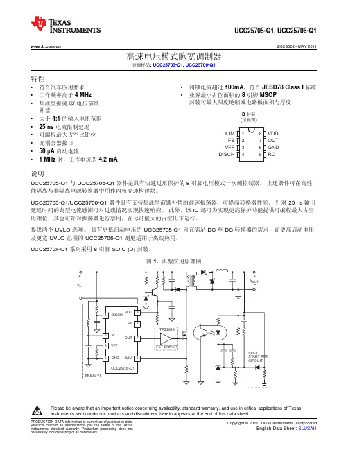
12348765ILIM FB VFF DISCHVDD OUT GND RCUCC25705-Q1,UCC25706-Q1ZHCS082–MAY 2011高速电压模式脉宽调制器查询样品:UCC25705-Q1,UCC25706-Q1特性•符合汽车应用要求•闭锁电流超过100mA ,符合JESD78Class I 标准•工作频率高于4MHz •业界最小占位面积的8引脚MSOP封装可最大限度地缩减电路板面积与厚度•集成型振荡器/电压前馈补偿D 封装•大于4:1的输入电压范围(顶视图)•25ns 电流限制延迟•可编程最大占空比钳位•光耦合器接口•50µA 启动电流•1MHz 时,工作电流为4.2mA说明UCC25705-Q1与UCC25706-Q1器件是具有快速过压保护的8引脚电压模式一次侧控制器。
上述器件可在高性能隔离与非隔离电源转换器中用作内核高速构建块。
UCC25705-Q1/UCC25706-Q1器件具有支持集成型前馈补偿的高速振荡器,可提高转换器性能。
针对25ns 输出延迟时间的典型电流感测可对过载情况实现快速响应。
此外,该IC 还可为实现更高保护功能提供可编程最大占空比钳位,其也可针对振荡器进行禁用,在尽可能大的占空比下运行。
提供两个UVLO 选项。
具有更低启动电压的UCC25705-Q1旨在满足DC 至DC 转换器的需求,而更高启动电压及更宽UVLO 范围的UCC25706-Q1则更适用于离线应用。
UCC2570x-Q1系列采用8引脚SOIC (D)封装。
图1.典型应用原理图Please be aware that an important notice concerning availability,standard warranty,and use in critical applications of Texas Instruments semiconductor products and disclaimers thereto appears at the end of this data sheet.UCC25705-Q1,UCC25706-Q1ZHCS082–ABSOLUTE MAXIMUM RATINGSover operating free-air temperature(unless otherwise noted)(1)(2)VALUE UNIT Supply voltage15VInput voltage(VFF,RC,ILIM)7VInput voltage(FB)15VInput current(DISCH)1mA Output current(OUT)dc±20mA Storage temperature,T stg–65to150°C Junction temperature,T J–55to150°CLead temperature(soldering,10sec)300°C (1)Stresses beyond those listed under“absolute maximum ratings”may cause permanent damage to the device.These are stress ratingsonly,and functional operation of the device at these or any other conditions beyond those indicated under“recommended operating conditions”is not implied.Exposure to absolute-maximum-rated conditions for extended periods may affect device reliability.(2)All voltages are with respect to GND.Currents are positive into,negative out of the specified terminal.Consult /packaging for moreinformation.RECOMMENDED OPERATING CONDITIONSover operating free-air temperature range(unless otherwise noted)VALUE UNITT A Operating ambient temperature–40to105°CORDERING INFORMATION TABLETOP-SIDE T A PACKAGE ORDERABLE PART NUMBERMARKING -–40°C to125°C SOIC-8–D Reel of2500UCC25706QDRQ125706Q-–40°C to125°C SOIC-8–D Reel of2500UCC25705QDRQ1PreviewESD RATINGS TABLEPARAMETER VALUE UNITHuman Body Model(HBM)1000V ESD Charged-Device Model(CDM)1000VMachine Model(MM)200VUCC25705-Q1,UCC25706-Q1 ZHCS082–MAY2011ELECTRICAL CHARACTERISTICSV DD=11V,V IN=30V,R T=47k,R DISCH=400k,R FF=14k,C T=220pF,C VDD=0.1µF,and no load on the outputs,T A= -–40°to125°C,(unless otherwise specified)PARAMETER TEST CONDITIONS MIN TYP MAX UNIT UVLO section(UCCx5705)Start threshold8.08.89.6V Stop threshold7.48.29.0V Hysteresis0.30.6 1.0V UVLO section(UCCx5706)Start threshold11.212.012.8V Stop threshold7.28.08.8V Hysteresis 3.2 4.0 4.5V Supply Current SectionStart-up current V DD=UVLO start–1V,V DD comparator off3090µAI DD active V DD comparator on,oscillator running at1MHz 4.2 5.0mA Line Sense SectionLow line comparator threshold0.95 1.00 1.15V Input bias current(VFF)–100100nA Oscillator SectionFrequency VFF=1.2V to4.8V0.9 1.0 1.1MHzVFF=1.2V,See(1) 1.2VCT peak voltageVFF=4.8V,See(1) 4.8VCT valley voltage See(1)0V Current Limit SectionInput bias current0.2–0.2–1µA Current limit threshold180200220mV Propagation delay,ILIM to OUT50mV overdrive2535ns Pulse Width Modulator SectionFB input impedance V FB=3V305090kΩMinimum duty cycle V FB<2V0%V FB=V DD,F OSC=1MHz707580% Maximum duty cycleV DISCH=0V,F OSC=1MHz93% PWM gain V FF=2.5V,MODE=112%/V Propagation delay,PWM to OUT65130ns Output SectionV OH I OUT=–5mA,V DD–output0.30.6VV OL I OUT=5mA0.150.4V Rise time C LOAD=50pF1025nsFall time C LOAD=50pF1025ns (1)Specified by design.FFFF DISCH 2R VFF VIN 2R R æö´»´ç÷´+èøUCC25705-Q1,UCC25706-Q1ZHCS082–MAY 2011PIN DESCRIPTIONSDISCH:A resistor to VIN sets the oscillator discharge current programming a maximum duty cycle.When grounded,an internal comparator switches the oscillator to a quick discharge mode.A small 100-pF capacitor between DISCH and GND may reduce oscillator jitter without impacting feed-forward performance.I DISCH must be between 25µA and 250µA over the entire V IN range.FB:Input to the PWM comparator.This pin is intended to interface with an optocoupler.Input impedance is 50-k Ωtypical.GND:Ground return pin.I LIM :Provides a pulse-by-pulse current limit by terminating the PWM pulse when the input is above 200mV.This provides a high speed (25ns typical)path to reset the PWM latch,allowing for a pulse-by-pulse current limit.OUT:The output is intended to drive an external FET driver or other high impedance circuits,but is not intended to directly drive a power MOSFET.This improves the controller ’s noise immunity.The output resistance of the PWM controller,typically 60Ωpull-up and 30Ωpull-down,will result in excessive rise and fall times if a power MOSFET is directly driven at the speeds for which the UCC2570x-Q1is optimized.RC:The oscillator can be configured to provide a maximum duty cycle clamp.In this mode the on-time is set by RT and CT,while the off-time is set by R DISCH and CT.Since the voltage ramp on CTis proportional to VIN,feed-forward action is obtained.Since the peak oscillator voltage is also proportional to VIN,constant frequency operation is maintained over the full power supply input range.When theDISCH pin is grounded,the duty cycle clamp is disabled.The RC pin then provides a low impedance path to ground CT during the off time.V DD :Power supply pin.This pin should be bypassed with a 0.1-µF capacitor for proper operation.The undervoltage lockout function of the UCC2570x-Q1allows for a low current startupmode and ensures that all circuits become active in a known state.The UVLO thresholds on the UCC25705-Q1are appropriate for a dc-to-dc converter application.The wider UVLO hysteresis of the UCC25706-Q1(typically 4V)is optimized for a bootstrap startup mode from a high impedance source.V FF :The feed-forward pin provides the controllerwith a voltage proportional to the power supply input voltage.When the oscillator is providing a duty cycle clamp,a current of 2×I DISCH is sourced from the V FF pin.A single resistor R FF between V FF and GND then set V FF to:When the DISCH pin is grounded and the duty cycle clamp is not used,the internal current source is disabled and a resistor divider from VIN is used to set VFF.In either case,when the voltage on V FF is less than 1.0V,both the output and oscillator are disabled.OUTVDDGND ILIMRCVFF FB DISCHUCC25705-Q1,UCC25706-Q1ZHCS082–MAY 2011Figure 2.Block DiagramFUNCTIONAL DESCRIPTIONOscillator and PWMThe oscillator can be programmed to provide a duty cycle clamp or be configured to run at the maximum possible duty cycle.The PWM latch is set during the oscillator discharge and is reset by the PWM comparator when the C T waveform is greater than the feedback voltage.The voltage at the FB pin is attenuated before it is applied to the PWM comparator.The oscillator ramp is shifted by approximately 0.65-V at room temperature at the PWM comparator.The offset has a temperature coefficient of approximately -–2mV/°C.The I LIM comparator adds a pulse by pulse current limit by resetting the PWM latch when V ILIM >200mV.The PWM latch is also reset by a low line condition (V FF <1.0V).All reset conditions are dominant;asserting any output will force a zero duty cycle output.Oscillator With Duty Cycle Clamp (MODE =1)The timing capacitor C T is charged from ground to V FF through R T .The discharge path is through an on-chip current sink that has a value of 30×I DISCH ,where I DISCH is the current through the external resistor R DISCH .Since the charge and discharge currents are both proportional to V IN ,their ratio,and the maximum duty cycle remains constant as V IN varies.FFV INFF FFON T T IN DISCHV 2R T R C where V R ´=a ´´a =»()T T DISCH OFF T DISCHC R ×R T 30R -R ´=a ´´1DISCHT T T DISCH11f R R C 30R -R =´a ´´+´ON DISCH ON OFF T T R Duty Cycle 1T T 30R æö==-ç÷+´èøUCC25705-Q1,UCC25706-Q1ZHCS082–MAY 2011Figure 3.Duty Cycle Clamp (MODE =1)The on-time is approximately:The off-time is:The frequency is:The maximum duty cycle is:FF(min)18V ==1.20V15IN(min)ON(max)T FF(min)TV T R V C ´=´TDISCH FF(min)T T IN(min)OFF(min)30R R V R C V1T ´=æöæö´´ç÷ç÷èøç÷+ç÷ç÷èø()FF(min)DISCHFF IN(min)V R R 2V 1´=´-UCC25705-Q1,UCC25706-Q1ZHCS082–MAY 2011Component Selection for Oscillator With Duty Cycle Clamp (MODE =1)For a power converter with the following specifications:•V IN(min)=18V •V IN(max)=75V •V IN(shutdown)=15V •F OSC =1MHz•MAX =0.78at V IN(min)In this mode,the on-time is approximately:•T ON(max)=780ns •T OFF(min)=220ns•1.Pick C T =220pF.2.Calculate R T .R T =51.1k Ω3.R DISCHR DISCH =383k Ω.I DISCH must be between 25µA and 250µA over the entire VIN range.With the calculated values,I DISCH ranges from 44µA to 193µA,within the allowable range.If I DISCH is toohigh,C T must be decreased.4.R FFThe nearest 1%standard value to the calculated value is 13.7k.V INFF ON T T INV T R C where V =a ´´a =T T 1f R C 75ns=a´´+UCC25705-Q1,UCC25706-Q1ZHCS082–MAY 2011Oscillator Without Duty Cyle Clamp (MODE =0)In this mode,the timing capacitor is discharged through a low impedance directly to ground.The DISCH pin is externally grounded.A comparator connected to DISCH senses the ground connection and disables both the discharge current source and V FF current source.A resistor divider is now required to set V FF .Figure 4.Ocsillator Without Clamp (MODE =0)In this mode,the on-time is approximately:The off-time is:T OFF ≈75ns The frequency is:FF(min)18V 1.2V 15==IN(min)FF(min)OSCT TV 175ns V F R C æö´-ç÷èø=UCC25705-Q1,UCC25706-Q1ZHCS082–MAY 2011Component Selection for Oscillator Without Duty Cycle Clamp (MODE =0)For a power converter with the following specifications:•V IN(min)=18V •V IN(max)=75V •V IN(shutdown)=15V •F OSC =1MHz With these specifications,1.Pick C T =220pF2.Calculate R T .-50-2525575100125Temperature –78910111213°CU V L O --T h r es h o l d s --V-502525575100125Temperature –8.08.18.28.38.48.58.68.78.88.9°CU V L O --Th r e s h o l d s --V--50-2525575100125Temperature –3.84.04.24.34.54.74.83.94.14.44.6°C I D D --m A-50-250255075100125Temperature 0.650.970.991.001.021.041.050.960.981.011.03–°CL o w -L i ne T h r e s h o l d --VUCC25705-Q1,UCC25706-Q1ZHCS082–MAY 2011TYPICAL CHARACTERISTICSUCC25705-Q1UVLO THRESHOLDSUCC25706-Q1UVLO THRESHOLDSvsvsTEMPERATURETEMPERATUREFigure 5.Figure 6.OPERATING CURRENT (AT 1MHz)LOW-LINE THRESHOLDvsvsTEMPERATURETEMPERATUREFigure 7.Figure 8.-50-25255075100125Temperature –0.901.001.100.951.05O s c i l l a t o r F r e q u e n c y --M H z°C-50-250255075100125Temperature 6876827078727480°CP r o g r a m m a b l e M a x i m u m D u t y C y c l e --%-50-2525575100125Temperature –180200220185205190195210215°C C u r r e n t -L i m i t T hr e s h o l d --m V-50-2525575100125Temperature –1525351729192331332127°CC u r r e n t -L i m i t P ro p D e l a y --n sUCC25705-Q1,UCC25706-Q1ZHCS082–MAY 2011TYPICAL CHARACTERISTICSPROGRAMMABLE MAXIMUMOSCILLATOR FREQUENCYDUTY CYCLEvsvsTEMPERATURETEMPERATUREFigure 9.Figure 10.CURRENT-LIMIT THRESHOLDCURRENT-LIMIT PROP DELAYvsvsTEMPERATURETEMPERATUREFigure 11.Figure 12.重要声明德州仪器(TI)及其下属子公司有权在不事先通知的情况下,随时对所提供的产品和服务进行更正、修改、增强、改进或其它更改,并有权随时中止提供任何产品和服务。
大雅迪克目录(中文)
SCLT6
4$-5# 4$-5#
4$-5#
4$-5#
4$-5#
4$-5#
4$-5#
CLT4,SCLT6系列的带刹车的型号的
4$-5# 4$-5#
4$-54
4$-54
4$-54
SCLT4
4$-54 4$-54
4$-54
4$-54
4$-54
4$-54 4$-54
4$,3"&#
4$,3$#
ࣜܕچɿ4$,3˘˘˘#
高性能·长寿命的丝杆(不使产生磨耗的技术)
·一般的认为长时间使用滑动丝杆·螺母会由于磨耗而产生消耗,但是根据使用方法也可以实现长
时间使用也不会产生消耗。
控制伺服马达【速度-推力特性】,使丝杆和螺母在磨耗界限曲线内动作(参照右表)。
所以、实现了丝杆和螺母之间的空隙有油膜形成的状态(金属之间没有摩擦)下使用,理论上没
ࡌܝท
1
1
ࡌܝท
1 1 1
滑台式电缸
型 式
最大推力 ʢ/ʣʢLHGʣɿUZQ
4$-54
4$-54
4$-54
4$-54
4$-54 4$-54
大 雅 迪 克 综合目录
大雅迪克电缸
可简单操作的伺服系统
64݄൛
节省能源的执行器的决定版!
简单! 低价! 节能!
简单接线!简单操作!
和气缸同等的价格
特长1ɹ和气缸相比较
ᶃ 通过简单的接线即可使用。
ᶄ 耗电量得到大幅度(1/3至1/10)削减。 ᶅ 24V直流电和ON/OFF信号即可进行动作。 ᶆ 不需要缓冲器和自动开关。 ᶇ 可以在设定的区域内输出信号。 ᶈ 没有油状烟雾的扩散。 ᶉ 免维护!能够长时间的运作。
2SC2570A中文资料(renesas)中文数据手册「EasyDatasheet - 矽搜」

单元
–
–
1.0
µA
–
–
1.0
µA
40
–
200
–
–
5.0
–
GHz
8
10
–
dB
–
1.5
3.0
dB
–
0.7
0.9
pF
–
11.5
dB
2
芯片中文手册,看全文,戳
2SC2570A
典型特征(T
1 000 (mW)
800
tot
总功耗
- 环境温度
600
A = + 25℃° ,除非另有规定)
自由空气
标记
芯片中文手册,看全文,戳
2SC2570A
电气特性(T
参数 直流特性 集电极截止电流 发射极截止电流
DC电流增益
射频特性 增益带宽产品 插入功率增益 噪声系数 输出电容 最大可用功率增益
A = +25°°C)
符号
测试条件
ICBO VCB = 10 V, I E = 0 mA时
IEBO h Note 1
FE
VEB = 1.0 V, I C = 0 mA时 VCE = 10 V, I C 能力= 20 mA
fT VCE = 10 V, I C 能力= 20 mA
S2 21e
VCE = 10 V, I C = 20毫安,F = 1千兆赫
NF VCE = 10 V, I C = 5毫安,F = 1千兆赫
600
mW
Tj
150
°C
Ts tg
65 to +150
°C
注意 自由空气
当处理 ,因为这些器件对静电放电敏感小心遵守注意事项 .
电源管理芯片UCC2582资料
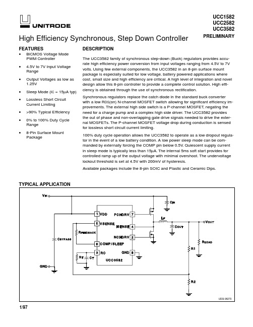
1/97TYPICAL APPLICATION•BiCMOS Voltage Mode PWM Controller • 4.5V to 7V Input Voltage Range•Output Voltages as low as 1.25V•Sleep Mode (I C = 15µA typ)•Lossless Short Circuit Current Limiting •>90% Typical Efficiency •0% to 100% Duty Cycle Range•8-Pin Surface Mount PackageHigh Efficiency Synchronous, Step Down ControllerFEATURESDESCRIPTIONUDG-96270UCC2582UCC3582PRELIMINARYThe UCC3582 family of synchronous step-down (Buck) regulators provides accu-rate high efficiency power conversion from input voltages ranging from 4.5V to 7V volts. Using few external components, the UCC3582 in an 8-pin surface mount package is especially suited for low voltage, battery powered applications where cost, small size and high efficiency are critical. A high level of integration and novel design allow this 8-pin controller to provide a complete control solution. High effi-ciency is obtained through the use of synchronous rectification.Synchronous regulators replace the catch diode in the standard buck converter with a low R DS (on) N-channel MOSFET switch allowing for significant efficiency im-provements. The external high side switch is a P-channel MOSFET , negating the need for a charge pump and a complex high side driver. The UCC3582 provides the out of phase and non-overlapping gate drive signals needed to drive the exter-nal MOSFETs. The P-channel MOSFET voltage drop during conduction is sensed for lossless short circuit current limiting.100% duty cycle operation allows the UCC3582 to operate as a low dropout regula-tor in the event of a low battery condition. A low power sleep mode can be com-manded by externally forcing the COMP pin below 0.5V . Quiescent supply current in sleep mode is typically less than 15µA. The internal 5ms soft start provides for controlled ramp up of the output voltage with minimal overshoot. The undervoltage lockout threshold is set at 4.5V with 200mV of hysteresis.Available packages include the 8-pin SOIC and Plastic and Ceramic Dips.ABSOLUTE MAXIMUM RATINGSSupply Voltage (VDD). . . . . . . . . . . . . . . . . . . . . . . . . . . . . . 7V Output Drivers (PCHDRV, NCHDRV) CurrentsContinuous . . . . . . . . . . . . . . . . . . . . . . . . . . . . . . . . ±0.25A Peak. . . . . . . . . . . . . . . . . . . . . . . . . . . . . . . . . . . . . ±500mA Inputs (VSENSE,COMP/SLEEP, RC, ISENSE). . −0.3V to 7V Storage Temperature. . . . . . . . . . . . . . . . . . . −65°C to +150°C Junction Temperature . . . . . . . . . . . . . . . . . . −55°C to +150°C Lead Temperature . . . . . . . . . . . . . . . . . . . . . . . . . . . . . +300°C All voltages with respect to GND. Currents are positive into, nega-tive out of the specified terminal. Pulsed is defined as a less than 10% duty cycle with a maximum duration of 500ns. Consult Pack-aging Section of Databook for thermal limitations and considera-tions of packages.CONNECTION DIAGRAMPARAMETERTEST CONDITIONSMINTYPMAXUNITSOverallSupply Current, Sleep V COMP = 0V1425µA Supply Current, Operating 1.53mA VCC Turn-on Threshold 4.5 4.75V VCC Turn-off Threshold 44.3VError Amplifier Input Voltage 1.23 1.25 1.27V VSENSE Bias Current –50025500nA Open Loop Gain V COMP = 1V to 3V 70100dB V OUT High R COMP = 100k to GND 4.3V V OUT LowR COMP = 100k to 5V0.7V Output Source Current VSENSE = 1.23V, V COMP = 4V –2mA Output Sink Current VSENSE = 1.27V, V COMP = 1V2mAOscillator Initial Accuracy T A = 25°C 180200 220kHz Voltage Stability VCC = 5V to 7V 1%Total Variation Line, Temperature175225kHz Ramp Amplitude (p-p) 3.6 4.2V Ramp Valley Voltage0.81.5VSleep, Soft Start, Current Limit Sleep Threshold Measured at V COMP 0.30.40.5V Sleep Input Bias Current V COMP = 0V–10µA Soft Start Time 2.557.5ms Reverse Current Offset 52035mV Current Limit ThresholdReference to V IN –360–450–540mVELECTRICAL CHARACTERISTICS: Unless otherwise specified, VCC = 5V, CT = 470pF, RT = 10k, TA = -55°C to 125°Cfor UCC1582, –25°C to 85°C for UCC2582, 0°C to 70°C for UCC3582, T A = T J .DIL-8, SOIC-8D, N and J PackagesCOMP/SLEEP: This is the output of the voltage amplifier.The voltage at this output is inverted internally and connected to the non-inverting input of the PWM comparator. A lead-lag network around the voltage amplifier compensates for the two pole LC filter characteristic inherent to voltage mode control, and is required in order to optimize the dynamic performance of the voltage mode control loop. Sleep mode is invoked if COMP is pulled and held below 0.5V which can be accomplished by an external gate or transistor. Sleep mode supply current is 15µA typical.GND: All voltages are measured with respect to this pin.All bypass and timing capacitors connected to GND should have leads as short and direct as possible.ISENSE : This input is connected to the junction between the two external power MOSFET transistors. The voltage drop across the upper P-channel device is monitored by ISENSE during conduction, and forms the current limit signal. When this drop exceeds 450mV the overcurrent comparator and logic sets the PWM latch and terminates the output pulse. The controller stops switching and goes through a soft start sequence. This prevents excess power dissipation in the NMOSFET during a short circuit.The reverse current comparator senses the drop across the lower N-channel MOSFET and disables the drive signal if a small positive voltage is present. A positive voltage is indicative of either P-channel conduction or reverse inductor current. T o disable the overcurrent comparator, connect ISENSE to VDD.PCHDRV , NCHDRV: The output drivers are rated for 0.5A peak currents. The PWM circuitry provides complementary drive signals to the output stages. Cross conduction of the external MOSFETs is prevented by monitoring the voltage on the P-channel and N-channel driver pins in conjunction with a time delay optimized for FET turn-off characteristics.RC: A parallel capacitor and resistor combination from RC to GND sets the PWM oscillator frequency according to the following equation:F ≈0.72RCUse a high quality ceramic capacitor with low ESL and ESR for best results. A minimum C T value of 200pF ensures good accuracy and less susceptibility to circuit layout parasitics. The waveform on RC has a fast linear charge and slow RC exponential discharge characteristic.The exponential characteristic improves converter response to input line voltage changes. The oscillator and PWM are designed to provide practical operation to 500kHz.VDD: Positive supply rail for the IC. Bypass this pin to GND with a 0.1 to 1µF low ESL/ESR ceramic capacitor. VSENSE: This pin is the inverting input of the voltage amplifier and serves as the output voltage feedback point for the Buck converter. It senses the output voltage through an external divider.PIN DESCRIPTIONSELECTRICAL CHARACTERISTICS: Unless otherwise specified, VCC = 5V, CT = 470pF, RT = 10k, TA = -55°C to 125°Cfor UCC1582, –25°C to 85°C for UCC2582, 0°C to 70°C for UCC3582, T A = T J .PARAMETERTEST CONDITIONSMINTYPMAXUNITSN-Channel and P-Channel Driver Outputs Output High Voltage I OUT = –50mA 4.04.5V Output Low Voltage I OUT = 50mA 0.5V Output Resistance I OUT = 100mA15ΩOutput Low (UVLO)I OUT = 10mA, VCC = 0V 0.9V Output Rise Time C OUT = 1nF 30ns Output Fall Time C OUT = 1nF 30ns Output Dead Time C OUT = 1nF200ns Overcurrent Blank Time 300ns Reverse Current Blank Time300nsBLOCK DIAGRAMUDG-95012-1 UNITRODE INTEGRA TED CIRCUITS7 CONTINENT AL BL VD.20 MERRIMACK, NH 03054TEL. (603) 424-2410 FAX (603) 424-3460。
ANSI C78.5-2003 自整流紧凑型荧光灯性能说明

ANSI C78.5-2003Revision of C78.5-1997 American National StandardApproved: November 19, 2003 Secretariat: ANSLG -National Electrical Manufacturers AssociationFor Electric LampsSpecifications forPerformance of Self-ballasted Compact Fluorescent LampsAmerican National Standard Approval of an American National Standard requires verification by ANSI that the requirements for due process, consensus, and other criteria for approval have been met by the standards developer. An American National Standard implies a consensus of those substantially concerned with its scope and provisions. Consensus is established when, in the judgment of the ANSI Board of Standards Review, substantial agreement has been reached by directly and materially affected interests. Substantial agreement means much more than a simple majority, but not necessarily unanimity. Consensus requires that all views and objections be considered, and that a concerted effort be made toward their resolution. The existence of an American National Standard does not in any respect preclude anyone, whether s/he has approved the standard or not, from manufacturing, marketing, purchasing, or using products, processes, or procedures not conforming to the standards. It is intended as a guide to aid the manufacturer, the consumer, and the general public.The American National Standards Institute does not develop standards and will in no circumstances give an interpretation of any American National Standard. Moreover, no person shall have the right or authority to issue an interpretation of an American National Standard in the name of the American National Standards Institute. Requests for interpretations should be addressed to the Committee Secretariat referred to on the title page.CAUTION NOTICE: This American National Standard may be revised or withdrawn at any time. The procedures of the American National Standards Institute require that action be taken periodically to reaffirm, revise, or withdraw this standard. Purchasers of American National Standards may receive current information on all standards by calling or writing the American National Standards Institute.Printed and distributed by:Information Handling Services/Global Engineering Documents 15 Inverness Way East, Englewood, CO 80112-5776Under Contract with National Electrical Manufacturers AssociationCopyright Ó2003 by American National Standard Lighting Group In Affiliation with National Electrical Manufacturers Association All rights reserved.No part of this publication may be reproduced in any form,in an electronic retrieval system or otherwise, withoutprior written permission of the publisher.Printed in the United States of AmericaForeword (This foreword is not part of American National Standard C78.5-2003)Suggestions for improvement of this standard should be submitted to the Secretariat C78, American National Standard Lighting Group (NEMA), 1300 North 17th Street, Suite 1847, Rosslyn, VA 22209.This standard was processed and approved by Accredited Standards Committee on Electric Lamps, C78, and its Sub-Committee, C78 WG 02. Committee approval of the standard does not necessarily imply that all committee members voted for that approval.Information concerning approval of this standard is based on the documents listed in the table below.Amendment / Change CDV RVRevision CDV C78(2)/4133 RV C78(2)/4134David Mullen, Chairman, C78David Mullen, Technical CoordinatorRandolph N. Roy, SecretariatMatthew C. Clark, Coordinating EditorTable of ContentsForeword5I. ScopeReferences 5 2. Normative6 3. DefinitionsGeneral 6 3.1maintenance 6 3.2Lumentemperatures 6 3.3Starting4. Requirements 64.1General 64.2 Marking 6markings 64.3Other6interference4.4Electro-magneticindex 7 rendering4.5Color7power4.6Input7timeStarting4.77time4.8Run-upLuminousflux 74.9maintenance 7 Lumen4.104.11 Efficacy 7Lifetest 74.12Powerquality 74.134.14 Lamp current operating frequency 7requirements 8 transient4.15Linespecimens 8 test5. Selectionof6. Tests 8General 8 6.1Supply 8 Power6.2Instruments 8 Electrical6.36.4 Lifetest 8Annex A (Informative) Guidance for the measurementof lamp starting time9Bibliography 10 (Informative)BAnnexSpecifications for Performance of Self-ballasted Compact Fluorescent Lamps1. ScopeThis standard specifies the performance requirements together with the test methods and conditions required to show compliance of self-ballasted compact fluorescent lamps up to 60 watts which are intended for domestic and similar general lighting purposes. Globe and reflector types are excluded. Such lamps shall have a rated input voltage of 120 or 127 volts at 60 Hz and an Edison screw base.2. Normative ReferencesThe following publications contain provisions which, through reference in this text, constitute provisions of this American National Standard. At the time of publication, the editions indicated were valid. All standards are subject to revision, and parties to agreements based on this American National Standard are encouraged to investigate the possibility of applying the most recent editions of the publications indicated below.ANSI C78.375-1997, Fluorescent lamps - Guide for Electrical MeasurementsCIE Publication 13.3-1995, Second edition, Method of measuring and specifying color rendering index of light sourcesCIE Publication 15.2 (1986), ColorimetryIESNA LM-65-2001, Approved method for Lifetesting of Compact Fluorescent LampsIESNA LM-66-2000, Approved method for the Electrical and Photometric Measurements of Single-ended Compact Fluorescent LampsUL 1993-1993, Standard for Self-Ballasted Lamps and Lamp AdaptersANSI C82.13-2002, Definitions – for fluorescent lamps and ballastsANSI C82.77-2002, Harmonic emission limits – related power quality requirements for lighting equipment3. Definitions3.1 GeneralSee ANSI C82.13 for related definitions. Any standards referenced in those definitions should be considered as normative for the standard. Other definitions used in this standard follow.3.2 Lumen maintenanceThe luminous flux at a given time in the life of the lamp and expressed as a percentage of the initial luminous flux. The mean lumens are the value at 40% of rated life.temperatures3.3 StartingThe minimum and maximum temperatures at which the lamp will reliably start.4. Requirements4.1 GeneralSelf-ballasted compact fluorescent lamps shall be so constructed that, in normal use, they are without danger to the user and the general surroundings.Electrical and photometric performance of compact fluorescent lamps can be appreciably affected by drafts, ambient temperature, and burning position. For proper measurements of these characteristics, the requirements of clause 4, Ambient conditions, and clause 8, Lamp stabilization, in ANSI C78.375 must be met. Photometric procedures are covered under clauses 9,10, and 11 of IESNA LM-66. The lamps shall be stabilized base-up at 25o C.4.2 MarkingThe unit shall be marked in accordance with clause 27 of UL1993, Standard for safety, Self-ballasted Lamps and Lamp Adaptors.4.3 Other markings4.3.1The unit shall include instructions per clause 28 of UL1993 if so required.4.3.2 A warning regarding possible interaction with IR remote controls may be needed on the packaging of some units.4.3.3If the luminous flux in other burning positions varies by more than 5% from the rated position it shall be marked on the packaging.interference4.4 Electro-magneticUnits with electronic high frequency circuits shall comply with FCC regulations, Title 47 of the US Code of Federal Regulations, Part 18 for Consumer equipment. For units with electronic high frequency circuits operating below 1.705 MHz, radiated measurements shall be made from 30 to 200 MHz and be under the limits specified in FCC Part 18.305c.4.5 Color rendering indexSelf-ballasted compact fluorescent lamps shall have a minimum rated CRI of 80 when measured in accordance with CIE Publication 13.3. The CRI value of an individual unit shall not be less than the rated value decreased by three.4.6 InputpowerThe input to the unit at rated supply voltage shall not exceed the rated value by more than 10% plus 0.5 watts.time4.7 StartingThe time to start when tested at the rated supply voltage in a 25+/-50 C ambient shall not exceed 2 seconds for electronic high frequency units and 4 seconds for magnetic units. The time to start for these units when tested at 90% of the rated supply voltage and at the minimum specified starting temperature shall not exceed 5 and 10 seconds respectively. Guidance for the measurement of starting time is given in Annex A.4.8 Run-up timeThe run-up time shall not exceed 3 minutes when tested at rated supply voltage in an ambient of 25 C.Flux4.9 LuminousThe initial luminous flux of the units tested shall average not less than 90% of the rated value.4.10 Lumen MaintenanceThe lumen maintenance at 40% of rated life shall not be less than 80%.4.11 EfficacyThe minimum rated efficacy of a self-ballasted compact fluorescent lamp shall be at least 40 lpw.4.12 LifetestLifetesting shall be done in accordance with the requirements on clauses 2, 3.2, 3.4, 5, and 6 of IESNA LM-65.4.13 Power QualityThe requirements for this product as specified in C82.77 shall be met.4.14 Lamp current operating frequencyTo limit incompatibility with infrared remote controls, the lamp current operating frequency shall be greater than 40 kHz for units with electronic high frequency circuits. These frequencies shall be met under all stable normal operating conditions including dimming.4.15 Line transient requirementsElectronic high-frequency ballasts are more susceptible to line transients than line frequency magnetic ballasts. Therefore, transient protection shall be included when lamps use electronic ballasts. The requirement for this transient protection is ANSI/IEEE C62.41, Class A1 minimum with the voltage increased to 2500Vpeak. The line transient test shall consist of seven strikes of a 100KHz Ring Wave, 2500Vp level, for differential mode. The transient generator effective output impedance shall be 30 ohms maximum and the peak current shall be 83A minimum.5. Selection of test specimens5.1Lamps shall be selected so as to ensure proper representation of the current design.5.2At least 3 specimens shall be procured for each sample. It is prudent to select one or more additional specimens to serve as potential replacements in the event of breakage or if the specimens become defective during the test for reasons not connected to the test, or if one or more specimens exhibit abnormal behavior or fail to stabilize.6. Tests6.1 General6.1.1Each test shall be performed at least once with each of the three specimens. Each specimen shall meet the described test criteria.6.1.2If a specimen breaks or becomes defective for reasons not as a result of the testing, the specimen shall be discarded. Similarly if a unit fails to stabilize or exhibits abnormal behavior, the lamp shall be discarded. Testing shall resume with a suitable replacement specimen procured and prepared in the same manner as the original specimen. The use of replacement specimens shall be documented in the test report.supply6.2 PowerFor other than lifetests, the voltage to the unit under test shall meet the requirements of clause 3, supply voltage characteristics in ANSI C78.375.instruments6.3 ElectricalThe electrical instruments used in the testing shall meet the requirements of clause 9, Instruments. in ANSI C78.375.6.4 LifetestTests to establish life ratings require a larger sample size. Guidance is given in IESNA LM-65 and the requirements cited above must be met.ANNEX A(Informative)Guidance for the measurement of lamp starting time1. Lamps shall be off and shall be stored at the specified ambient test temperature for at least 12 hours prior to the test.2. No starting aid plane shall be used for the test.3.The recommended method to detect lamp starting is to monitor lamp light output.4. A photodetector must be located such that it will adequately respond to the lamp light output. Shielding from extraneous light may be required.5. The laboratory should establish a responsive and repeatable set-up with their equipment and a documented test procedure prior to the test. This may include a qualification procedure for the operator.6. Some lamps may contain a mercury amalgam that will delay the rise to full light output. This should not be interpreted as a delay in the starting time. The lamp should be considered as fully lighted if it is operating at essentially full current even if the light output is not uniform throughout the bulb.7. A digital storage scope is recommended for monitoring the time from application of the test voltage and the output of the photo detector and the lamp input current.8.Monitoring the lamp input current and/or wattage can also be an accurate method to test starting time but it may require more knowledge of lamps and judgement on the part of the operator. This alternate is acceptable if correlation to the recommended method is documented.Annex B(Informative)BibliographyIEC 60969-1988, Self-ballasted lamps for general lighting service, performance requirementsIEC 60968-1988, Self -ballasted lamps for general lighting service, safety requirements CSA C861-1995, Performance of Compact Fluorescent Lamps and Ballast Adaptors IESNA Lighting Handbook, ninth edition。
UCC35702中文资料

13.5 13
200 190 1.5 15 15
4.9
5.1
50
2
元器件交易网
UCC15701/2 UCC25701/2 UCC35701/2 ELECTRICAL CHARACTERISTICS: Unless otherwise specified, VDD = 11V, RT = 60.4k, CT = 330pF, CREF = CVDD = 0.1 F, VFF = 2.0V, and no load on the outputs.
Note: All voltages are with respect to GND. Currents are positive into the specified terminal. Consult Packaging Section of the Databook for thermal limitations and considerations of packages.
TYPICAL APPLICATION DIAGRAM
VIN SUPPLY
R1 R2 6 R3 7 VREF R4 9 R5 CS 14 CF 1 C3 RF R8 8 FB GND 13 R11 C5 12 VREF PGND 5 COUNT SS 11 VSCLAMP SYNC OUT ILIM 4 CT 10 CT RT UCC35701 VFF VDD 3
13V / 9V 0°C to +70°C 9.6V / 8.8V
CONNECTION DIAGRAMS
DIL-14, SOIC-14, TSSOP-14 (TOP VIEW) N or J, D, PW PACKAGE
COUNT ILIM VDD OUT PGND VFF RT 1 2 3 4 5 6 7 14 13 12 11 10 9 8 SS GND VREF SYNC CT VSCLAMP FB
- 1、下载文档前请自行甄别文档内容的完整性,平台不提供额外的编辑、内容补充、找答案等附加服务。
- 2、"仅部分预览"的文档,不可在线预览部分如存在完整性等问题,可反馈申请退款(可完整预览的文档不适用该条件!)。
- 3、如文档侵犯您的权益,请联系客服反馈,我们会尽快为您处理(人工客服工作时间:9:00-18:30)。
Note: All voltages are with respect to GND. Currents are positive into the specified terminal. Consult Packaging Section of the Databook for thermal limitations and considerations of packages.
DESCRIPTION
The UCC35701/UCC35702 family of pulse width modulators is intended for isolated switching power supplies using primary side control. They can be used for both off-line applications and DC/DC converter designs such as in a distributed power system architecture or as a telecom power source. The devices feature low startup current, allowing for efficient off-line starting, yet have sufficient output drive to switch power MOSFETs in excess of 500kHz. Voltage feed forward compensation is operational over a 5:1 input range and provides fast and accurate response to input voltage changes over a 4:1 range. An accurate volt-second clamp and maximum duty cycle limit are also featured. Fault protection is provided by pulse by pulse current limiting as well as the ability to latch off after a programmable number of repetitive faults has occurred. Two UVLO options are offered. UCC35701 family has turn-on and turn-off thresholds of 13V/9V and UCC35702 family has thresholds of 9.6V/8.8V. The UCC35701/2 and the UCC25701/2 are offered in the 14 pin SOIC (D), 14 pin PDIP (N) or in 14 pin TSSOP (PW) packages. The UCC15701/2 is offered in the 14 pin CDIP (J) package.
Supply voltage (Supply current limited to 20mA) . . . . . . . . 15V Supply Current. . . . . . . . . . . . . . . . . . . . . . . . . . . . . . . . . 20mA Input pins ( ILIM,VFF,RT,CT,VSCLAMP,SYNC,SS) . . . . . . 6V Output Current (OUT) DC. . . . . . . . . . . . . . . . . . . . . +/–180mA Output Current (OUT) Pulse (0.5ms) . . . . . . . . . . . . . . +/–1.2A Storage Temperature. . . . . . . . . . . . . . . . . . . –65°C to +150°C Junction Temperature . . . . . . . . . . . . . . . . . . . –55°C to +150°C Lead Temperature (Soldering, 10 sec.) . . . . . . . . . . . . +300°C
R6 R7
C6 VOUT C1 R8 R10 2 C2 RCS C4
RGND
VIN RETURN
VOUT R13
R12
C6 C7
R14 R15
UDG-98005-1
SLUS293A - JANUARY 2000
元器件交易网
UCC15701/2 UCC25701/2 UCC35701/2 ABSOLUTE MAXIMUM RATINGS
TYPICAL APPLICATION DIAGRAM
VIN SUPPLY
R1 R2 6 R3 7 VREF R4 9 R5 CS 14 CF 1 C3 RF R8 8 FB GND 13 R11 C5 12 VREF PGND 5 COUNT SS 11 VSCLAMP SYNC OUT ILIM 4 CT 10 CT RT UCC35701 VFF VDD 3
PARAMETER UVLO Section Start Threshold Stop Threshold Hysteresis Supply Current Start-up Current IDD Active VDD Clamp Voltage VDD Clamp – Start Threshold Voltage Reference VREF Line Regulation Load Regulation Short Circuit Current (UCCX5701) (UCCX5702) (UCCX5701) (UCCX5702) (UCCX5701) (UCCX5702) (UCCX5701) VDD = 11V, VDD Comparator Off (UCCX5702) VDD = 8V, VDD Comparator Off VDD Comparator On (UCCX5701) IDD = 10mA (UCCX5702) IDD = 10mA (UCCX5701) (UCCX5702) VDD = 10V to 13V, IVREF = 0mA to 2mA VDD = 10V to 13V IVREF = 0mA to 2mA VREF = 0V, TJ = 25°C TEST CONDITIONS MIN 12 8.8 8 8.0 3 0.3 TYP 13 9.6 9 8.8 4 0.8 130 120 0.75 14.3 13.8 1.3 4.2 5 20 2 20 MAX UNITS 14 10.4 10 9.6 V V V V V V µA A mA V V V V V mV mV mA
元器件交易网
application INFO available
UCC15701/2 UCC25701/2 UCC35701/2
Advanced Voltage Mode Pulse Width Modulator
FEATURES
• 700kHz Operation • Integrated Oscillator/ Voltage Feed Forward Compensation • Accurate Duty Cycle Limit • Accurate Volt-second Clamp • Optocoupler Interface • Fault Counting Shutdown • Fault Latch off or Automatic Shutdown • Soft Stop Optimized for Synchronous Rectification • 1A Peak Gate Drive Output • 130µA Start-up Current • 750µA Operating Current
13V / 9V 0°C to +70°C 9.6V / 8.8V
CONNECTION DIAGRAMS
DIL-14, SOIC-14, TSSOP-14 (TOP VIEW) N or J, D, PW PACKAGE
COUNT ILIM VDD OUT PGND VFF RT 1 2 3 4 5 6 7 14 13 12 11 10 9 8 SS GND VREF SYNC CT VSCLAMP FB
The D and PW packages are available taped and reeled. Add TR suffix to the device type (e.g., UCC35701DTR).
ELECTRICAL CHARACTERISTICS: Unless otherwise specified, VDD = 11V, RT = 60.4k, CT = 330pF, CREF = CVDD = 0.1 F, VFF = 2.0V, and no load on the outputs.
ORDERING INFORMATION
UVLO Option 13V / 9V –55°C to +125°C 9.6V / 8.8V 13V / 9V –40°C to +85°C 9.6V / 8.8V TA = TJ Package Part Number CDIP-14 CDIP-14 SOIC-14 PDIP-14 TSSOP-14 SOIC-14 PDIP-14 TSSOP-14 SOIC-14 PDIP-14 TSSOP-14 SOIC-14 PDIP-14 TSSOP-14 UCC15701J UCC15702J UCC25701D UCC25701N UCC25701PW UCC25702D UCC25702N UCC25702PW UCC35701D UCC35701N UCC35701PW UCC35702D UCC35702N UCC35702PW