RT2N62M中文资料
MHW6222中文资料

REV 6
RF DEVICE DATA ©MOTOROLA Motorola, Inc. 1994
MHW6222 1
元器件交易网
PACKAGE DIMENSIONS
–A– S –Z– –F– J V
Q
2 PL
0.25 (0.010)
M
T F
M
A
M
NOTES: 1. DIMENSIONING AND TOLERANCING PER ANSI Y14.5M, 1982. 2. CONTROLLING DIMENSION: INCH. DIM A B C D E F G J K L N P Q R S U V W INCHES MIN MAX ––– 1.775 ––– 1.085 ––– 0.840 0.018 0.022 0.465 0.510 0.300 0.325 0.100 BSC 0.156 BSC 0.315 0.355 1.00 BSC 0.165 BSC 0.100 BSC 0.148 0.168 ––– 0.595 1.500 BSC 0.200 BSC 0.280 BSC 0.435 0.450 MILLIMETERS MIN MAX ––– 45.08 ––– 27.56 ––– 21.34 0.46 0.56 11.81 12.95 7.62 8.25 2.54 BSC 3.96 BSC 8.00 8.50 25.40 BSC 4.10 BSC 2.54 BSC 3.76 4.27 ––– 15.11 38.10 BSC 5.08 BSC 7.11 BSC 11.05 11.43
CASE 714–06 ISSUE K
Motorola reserves the right to make changes without further notice to any products herein. Motorola makes no warranty, representation or guarantee regarding the suitability of its products for any particular purpose, nor does Motorola assume any liability arising out of the application or use of any product or circuit, and specifically disclaims any and all liability, including without limitation consequential or incidental damages. “Typical” parameters can and do vary in different applications. All operating parameters, including “Typicals” must be validated for each customer application by customer’s technical experts. Motorola does not convey any license under its patent rights nor the rights of others. Motorola products are not designed, intended, or authorized for use as components in systems intended for surgical implant into the body, or other applications intended to support or sustain life, or for any other application in which the failure of the Motorola product could create a situation where personal injury or death may occur. Should Buyer purchase or use Motorola products for any such unintended or unauthorized application, Buyer shall indemnify and hold Motorola and its officers, employees, subsidiaries, affiliates, and distributors harmless against all claims, costs, damages, and expenses, and reasonable attorney fees arising out of, directly or indirectly, any claim of personal injury or death associated with such unintended or unauthorized use, even if such claim alleges that Motorola was negligent regarding the design or manufacture of the part. Motorola and are registered trademarks of Motorola, Inc. Motorola, Inc. is an Equal Opportunity/Affirmative Action Employer.
T62M0002A中文资料

T62M0002ADigital Sound Processor EmbeddedSRAMFeatures! Operating voltage: 4.5V ~ 5.5V! ADM algorithm! Low noise ( -88dB typical)! Low distortion rate (0.5% typical)! Embedded SRAM! Automatic reset function! Package type: 16-pin DIP/SOP DescriptionThe T62M0002A is an echo/surround effect processor. It is designed for various audio systems including karaoke, television, sound equipment, etc. The chip consists of a built-in pre-amplifier, VCO or V oltage control OSC, Embedded SRAM, A/D and D/A converters as well as delay time control logic. Itsbuilt-In reply to SRAM can generate delay time effect and can control the delay time value through the external VCO resistor. The VCO circuit can reduce external components and make it easy to adjust the delay time.Part Number ExamplesPart NO. Pkg DescriptionT62M0002A-j 16-SOP 300mil-16-SOPT62M0002A-K 16-DIP 300mil-16-DIPTM Technology Inc. reserves the right P. 1 Publication Date: JUL. 2002TM Technology Inc. reserves the right P. 2 Publication Date: JUL. 2002 Block DiagramLP F1 INLP F1O UTLP F2O UTLP F2INO P 2O UTO P 2IN O P 1INO P 1O UTC C 0C C 1V C C R EF A GN DD GN D O S C _O V C OPIN ConfigurationT62M0002ATM Technology Inc. reserves the right P. 3 Publication Date: JUL. 2002 PIN DescriptionPin NO. Pin Name I/O Description 1 VCC - Analog and positive power supply 2 REF I Analog reference voltage 3 AGEND - Analog ground 4 DGEND - Digital ground 5 OSC_O I System oscillator output 6 VCO I System oscillator input,system frequency adjustable pin 7 CC1 - Currentcontrol18 CC2- Currentcontrol2 9 OP1_OUT O OP1output 10 OP1_IN I OP1 input 11 OP2_IN I OP2 input 12 OP2_OUT O OP2 output 13 LPF2_IN I Low pass filter2 input 14 LPF2_OUT O Low pass filter2 output 15 LPF1_OUT O Low pass filter1 output 16 LPF1_IN I Low pass filter1 inputFunction DescriptionThe T62M0002A is an echo/surround effect generator with built-in SRAM. It enaures low distortion as well as low noise for processing audio signal delay. The chip provides two playing modes(echo and surround) and the playing function block diagrams are shown as follows.- Surround Modeout -Echo ModeElectrical CharacteristicsTa=25ºC Symbol ParameterMin. Typ. Max. UnitTest ConditionsVDD ConditionsV oltage - - 4.5 5.0 5.5 V V CC OperatingCurrent 5V - - 15 30 mAI CC OperatingGain 5V RG V V oltage=47KΩ- 0.5 2.5 dBLV OMAX Maximum Output V oltage 5V THD=10% 1.0 1.6 - Vrms THD Total Harmonic Distortion 5V 30KHz L.P.F. - 0.5 1.5 %No Output Noise V oltage 5V DIN Audio - -88 -80 dbV Absolute Maximum RatingsSupply V oltage …………………………………………………. -0.3V to 6VInput V oltage …………………………………………………… Vss-0.3V to VDD+0.3VStorage Temperature ……………………………………………. -50ºC to 125ºCOperating Temperature ……………………………… -20ºC to 70ºCNote: These are stress ratings only. Stresses exceeding the range specified under “Absolute Maximum Ratings” may cause substantial damage to the device. Functional operation of this device at other conditions beyond those listed in the specification is not implied and prolonged exposure to extreme conditions may affect device reliability.TM Technology Inc. reserves the right P. 4 Publication Date: JUL. 2002Application CircuitsNote:”Radj” Value con set delay time. R/delay time Reference on Resistance / Delay Time Table.TM Technology Inc. reserves the right P. 5 Publication Date: JUL. 2002TM Technology Inc. reserves the right P. 6 Publication Date: JUL. 2002 Resistance / Delay Time Table .FCK 2.0M 2.5M 3.0M 3.5M 4.0M 4.5M 5.0M 5.5M Radj 53.40k 41.97k 33.41k 28.18k 24.00k 20.90k 18.20k 16.00k TD 264ms 226ms 174ms 150ms 130ms 117ms 106ms 95.2ms THD+N% 1.29% 0.95% 0.73% 0.57% 0.48% 0.41% 0.37% 0.33%FCK 6.0M 6.5M 7.0M 7.5M 8.0M 8.5M 9.0M 10M Radj 14.50k 12.90k 11.60k 10.70k 9.72k 9.07k 8.07k 6.98k TD 89ms 80.8ms 74.8ms 70.4ms 65.2ms 62.4ms 57.6ms 52.4ms THD+N% 0.29% 0.28% 0.25% 0.24% 0.22% 0.22% 0.21% 0.18%FCK 11M 12M 13M 14M 15M 16M 17M 18M Radj 5.99k 5.30k 4.52k 4.02k 3.48k 3.08k 2.64k 2.30k TD 47.6ms 44.2ms 40.2ms 37.6ms 35.0ms 33.0ms 30.8ms 29.0ms THD+N% 0.17% 0.15% 0.14% 0.14% 0.14% 0.14% 0.14%0.14%FCK 19M 20M 21M 22M Radj 2.16k 1.89k 1.69k 1.49k TD 27.8ms 26.2ms 25.0ms 24.0ms THD+N%0.14% 0.14% 0.14% 0.14%Note :This Table is for Surround Mode.R= Extend Resister for adjust FCK & TD.FCK= Oscillate output Frequency for Pin 5 .(Unit : MHZ) TD=Delay Time for output.THD=Total Harmonic Distortion. (TDH+N Ratio %)Pulse Clock Waveform for input PinTM Technology Inc. reserves the rightP. 7 Publication Date: JUL. 2002 IC PackageT62M0002A 16-SOPUnit:mmT62M0002A 16-DIPUnit:mm。
MSTP介绍

S4.1, L4.1, L4.2, CWDM SFP模块
2个 SFP接口可以同时插:
1 或 2个STM-1;
1 或 2个STM-4;
1个STM-1 + 1个STM-4.
组网灵活,节省业务板卡槽位
Page 36
1662SMC 高集成度板卡
板卡集成度
1×STM-16板卡
设备EPS保护
8×155M电 板卡支持 7:1保护
相同的板卡
2×STM-4板卡
8×STM-1 板卡 4×STM-1 板卡
63×2M板卡支持 2×3:1保护 电源1+1保护 矩阵1+1保护
3×34M板卡
3×45M板卡 63×2M板卡
网络保护
MS-SPRing, MSP SNCP/I , SNCP/N
PORT PORT PORT
PORT
2.5 Gbps backpanel
1660SM 子架视图
8
9
10G PORT PORT 10G PORT PORT
22 21 23
6
7
5
Access LS/HS
Access LS/HS Access LS/HS Access LS/HS Access LS
2
3
4
Page 8
2
Page 17
1660SM
1660SM 10G系统介绍
矩阵容量:
640x640 VC4 (100G HO) 16128x16128 VC12 (40G LO)
接口:
最大 4 x STM-64 最大 16 x STM-16 最大 64 x STM-4 最大 256 x STM-1 或 155M电 最大 48 x 34/45Mbit/s 最大 378 x 2Mbit/s 最大 112 x 10/100 Mb/s E/FE接口 最大 32个GE接口
WM2M054JPAR600;WM2F054WPAR300;WM2M054JPA;中文规格书,Datasheet资料

4/4
分销商库存信息:
JAE-ELECTRONICS WM2M054JPAR600 WM2F054WPAR300 WM2M054JPA
General Specifications
No. of contacts: 54 pos. Contact resistance: 50m ohm max. Dielectric withstanding voltage : AC250 per minute Operating temperature: -40 Deg. C to +85 Deg. C Rated voltage: 0.5A/ per pin Durability: 10,000 cycle
MB-0139-2
Plug side: WM2M054JPA (SJ100658)
Notice: Products shown in this leaflet are
Applicable P.C.B dimension
Japan Aviation Electronics Industry, Limited
/
JAE PMK Div. Proprietary. Copyright © 2006,Japan Aviation Electronics Industry, Ltd.
1/4
MB-0139-2
Materials and Finishes
Components Materials /Finishes Receptacle Copper Alloy/ Contact: 0.1um min. Au plating over Ni Terminal: Au flash plating over Ni Glass filled LCP (UL94V-0) Stainless steel Plug Copper Alloy/ Contact: 0.1um min. Au plating over Ni Terminal: Au flash plating over Ni Glass filled LCP Stainless steel Steel/ Ni plating M2
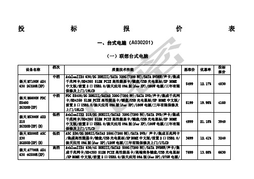
投标报价表
30%
4199
清华同方-超扬A500
-CPU:酷睿E5200 主板主控芯片组:945 内存:2G DDR2 800 网卡、声卡:集成光驱:DVD 硬盘:320G SATA 显示器:19WLCD 显示卡:集成键盘:标准鼠标:光电是否为自主创新产品:是是否是节能产品政府采购清单中的产品:是是否为环境标志产品:是
4399
9.09%
3999
A600
中档
T4400 /4G DDRIII 1066内存/500G/ATI HD4650 256MB 128bit显卡 /Slot-in Rambo /802.11b/g无线网卡 /千兆有线网卡/无线键鼠套装 /6合一读卡器 /集成1394 /集成摄像头 /集成麦克/集成2.1音箱 /3+3服务(含LCD)/ DOS for Win7 /21.5" FHD LCD显示屏(16:9)
4499
30%
3149
清华同方-超扬A300
-CPU:酷睿E3200 主板主控芯片组:945 内存:1G DDR2 667 网卡、声卡:集成光驱:DVD 硬盘:250G SATA 显示器:19WLCD 显示卡:集成键盘:标准鼠标:光电是否为自主创新产品:是是否是节能产品政府采购清单中的产品:是是否为环境标志产品:是其他:新超扬多功能机箱/ LINUX
6499
8.45%
5950
AIO B500
中档
PD E6300/2G DDRIII 1066内存/500G/ Geforce G210M 512MB DDRIII显存/ Tray-in Rambo /802.11b/g/n无线网卡/百兆有线网卡/有线键鼠套装/集成读卡器/集成摄像头/集成麦克/集成JBL2.0音箱/3+3服务(含LCD)/ DOS for Win7 /23"全高清LCD显示屏(16:9)
HM62W16256B中文资料

Read Cycle
, , , , ,,,,
Dout 50 pF 1.4 V HM62W16256B -5 -7 Max — 55 55 55 35 — 55 — — — — 20 20 20 20 Min 70 — — — — 10 — 10 10 5 5 0 0 0 0 Max — 70 70 70 40 — 70 — — — — 25 25 25 25 Unit ns ns ns ns ns ns ns ns ns ns ns ns ns ns ns 2, 3 2, 3 2, 3 2, 3 1, 2, 3 1, 2, 3 1, 2, 3 1, 2, 3 Notes Symbol t RC t AA t ACS1 t ACS2 Min 55 — — — — 10 — 10 10 5 5 0 0 0 0 t OE t OH t BA t CLZ1 t CLZ2
1 2
Unit V V W °C °C
Notes: 1. VT min: –3.0 V for pulse half-width ≤ 30 ns. 2. Maximum voltage is +4.6 V.
DC Operating Conditions
Parameter Supply voltage Symbol VCC VSS Input high voltage Input low voltage Ambient temperature range Note: VIH VIL Ta Min 3.0 0 2.0 –0.3 0 Typ 3.3 0 — — — Max 3.6 0 VCC + 0.3 0.8 70 Unit V V V V °C 1 Note
Capacitance (Ta = +25°C, f = 1.0 MHz)
M295V100-T120XM6R资料

AI0197416A0-A15W DQ0-DQ14V CCM29F100T M29F100BE V SS15G RPDQ15A–1BYTE RBFigure 1.Logic DiagramM29F100T M29F100B1Mbit (128Kb x8or 64Kb x16,Boot Block)Single Supply Flash Memory5V ±10%SUPPLY VOLTAGE for PROGRAM,ERASE and READ OPERATIONS FAST ACCESS TIME:70ns FAST PROGRAMMING TIME–10µs by Byte /16µs by Word typicalPROGRAM/ERASE CONTROLLER (P/E.C.)–Program Byte-by-Byte or Word-by-Word –Status Register bits and Ready/Busy Output MEMORY BLOCKS–Boot Block (Top or Bottom location)–Parameter and Main blocksBLOCK,MULTI-BLOCK and CHIP ERASE MULTI-BLOCK PROTECTION/TEMPORARY UNPROTECTION MODESERASE SUSPEND and RESUME MODES –Read and Program another Block during Erase SuspendLOW POWER CONSUMPTION –Stand-by and Automatic Stand-by100,000PROGRAM/ERASE CYCLES per BLOCK20YEARS DATARETENTION –Defectivity below 1ppm/year ELECTRONIC SIGNATURE –Manufacturer Code:0020h–Device Code,M29F100T:00D0h –Device Code,M29F100B:00D1hDESCRIPTIONThe M29F100is a non-volatile memory that may be erased electrically at the block or chip level and programmed in-system on a Byte-by-Byteor Word-by-Word basis using only a single 5V V CC supply.For Program and Erase operations the necessary high voltages are generated internally.The device can also be programmed in standard program-mers.The array matrix organisation allows each block to be erased and reprogrammed without affecting other blocks.Blocks can be protected against pro-graming and erase on programming equipment,and temporarily unprotected to make changes in the application.Each block can be programmed and erased over 100,000cycles.July 19981/30441SO44(M)TSOP48(N)12x 20mmDQ3DQ9DQ2A6DQ0W A3RB DQ6A8A9DQ13NC A10DQ14A2DQ12DQ10DQ15A–1V CC DQ4DQ5A7DQ7NC NC AI01975M29F100T M29F100B (Normal)121132425363748DQ8NC NC A1NC A4A5DQ1DQ11G A12A13NC A11BYTE A15A14V SSE A0RP V SS Figure 2A.TSOP Pin ConnectionsG DQ0DQ8A3A0E V SS A2A1A13V SSA14A15DQ7A12NC BYTE DQ15A–1DQ5DQ2DQ3V CCDQ11DQ4DQ14A9W RB A4NC RPA7AI01977M29F100T M29F100B 8234567910111213141516323130292827262524232220191817DQ1DQ9A6A5DQ6DQ134439383736353433A11A10DQ1021DQ12404314241NC A8Figure 2C.SO Pin Connections DQ3DQ9DQ2DQ0DQ6DQ13DQ14DQ12DQ10DQ15A–1V CC DQ4DQ5DQ7AI01976M29F100T M29F100B (Reverse)121132425363748DQ8DQ1DQ11NC BYTE V SS A0V SS A6A3A8A9NC A10A2A7NC NC NC NC A1NC A4A5A12A13A11A15A14RP W RB G EFigure 2B.TSOP Reverse Pin ConnectionsA0-A15Address InputsDQ0-DQ7Data Input/Outputs,Command Inputs DQ8-DQ14Data Input/OutputsDQ15A–1Data Input/Output or Address Input E Chip Enable G Output Enable W Write EnableRP Reset /Block Temporary Unprotect RB Ready/Busy Output BYTE Byte/Word Organisation V CC Supply Voltage V SSGroundTable 1.Signal NamesWarning:NC =Not Connected.Warning:NC =Not Connected.Warning:NC =Not Connected.2/30M29F100T ,M29F100BSymbol Parameter Value Unit T A Ambient Operating Temperature(3)–40to125°CT BIAS Temperature Under Bias–50to125°CT STG Storage Temperature–65to150°CV IO(2)Input or Output Voltages–0.6to7VV CC Supply Voltage–0.6to7V V(A9,E,G,RP)(2)A9,E,G,RP Voltage–0.6to13.5V Notes:1.Except for the rating”Operating Temperatur e Range”,stresses above those listed in the Table”Absolute Maximum Ratings”may cause permanent damage to the device.These are stress ratings only and operation of the device at these or any otherconditions above those indicated in the Operating sections of this specification is not implied.Exposure to Absolute MaximumRating conditions for extended periods may affect device reliability.Refer also to the STMicroelectronics SURE Program and other relevant quality documents.2.Minimum Voltage may undershoot to–2V during transition and for less than20ns.3.Depends on range.Table2.Absolute Maximum Ratings(1)Instructions for Read/Reset,Auto Select for read-ing the Electronic Signature or Block Protection status,Programming,Blockand ChipErase,Erase Suspend and Resume are written to the device in cyclesof commandsto a CommandInterfaceusing standard microprocessor write timings.The device is offered in TSOP48(12x20mm)and SO44packages.Both normal and reverse pinouts are available for the TSOP48package. OrganisationThe M29F100is organised as128Kb x8or64Kb x16bits selectable by the BYTE signal.When BYTE is Low the Byte-wide x8organisation is selected and the address lines are DQ15A–1and A0-A15.The Data Input/Output signal DQ15A–1 acts as address line A–1which selects the lower or upper Byte of the memory word for output on DQ0-DQ7,DQ8-DQ14remain at High impedance. When BYTE is High the memory uses the address inputs A0-A15and the Data Input/Outputs DQ0-DQ15.Memory control is provided by Chip Enable E,Output Enable G and Write Enable W inputs. AReset/Block TemporaryUnprotection RPtri-level input provides a hardware reset when pulled Low, andwhen heldHigh(atV ID)temporarily unprotects blocks previously protected allowing them to be programedand erased.Erase and Program opera-tions are controlled by an internal Program/Erase Controller(P/E.C.).Status Register data output on DQ7provides a Data Polling signal,and DQ6and DQ2provide Toggle signals to indicate the state of the P/E.C operations.A Ready/Busy RB output indicates the completion of the internal algorithms. Memory BlocksThe devices feature asymmetrically blocked archi-tectureproviding system memory integration.Both M29F100T and M29F100B devices have an array of5blocks,one Boot Block of16KBytes or8 KWords,two Parameter Blocks of8KBytes or4 KWords,one Main Block of32KBytes or16 KWords and one Main Blocks of64KBytes or32 KWords.The M29F100T has the Boot Block at the top of the memory address space and the M29F100B locates the Boot Block starting at the bottom.The memory maps are showed in Figure 3.Each block can be erased separately,any com-bination of blocks can be specified for multi-block erase or the entire chip may be erased.The Erase operations are managed automatically by the P/E.C.The block erase operation can be sus-pended in order to read from or program to any block not being ersased,and then resumed. Block protection provides additional data security. Each block can be separately protected or unpro-tected against Program or Erase on programming equipment.All previously protected blocks can be temporarily unprotected in the application.Bus OperationsThe following operations can be performed using the appropriatebus cycles:Read(Array,Electronic Signature,Block Protection Status),Write com-mand,Output Disable,Standby,Reset,Block Pro-tectio n,Unp ro te ctio n,Pro te cti on Verify, Unprotection Verify and Block Temporary Unpro-tection.See Tables4and5.DESCRIPTION(Cont’d)3/30M29F100T,M29F100B16K BOOT BLOCKAI019781FFFFh1C000h 1BFFFh1A000h 19FFFh 8K PARAMETER BLOCK8K PARAMETER BLOCK32K MAIN BLOCK 64K MAIN BLOCKM29F100T18000h 17FFFh 10000h 0FFFFh 00000hM29F100B 16K BOOT BLOCK8K PARAMETER BLOCK 8K PARAMETER BLOCK 32K MAIN BLOCK 64K MAIN BLOCK 1FFFFh10000h 0FFFFh 08000h 07FFFh 04000h 03FFFh 00000h 06000h 05FFFh Figure 3.Memory Map and Block Address Table (x8)Address Range (x8)Address Range (x16)A15A14A13A1200000h-03FFFh 0000h-1FFFh 000X 04000h-05FFFh 2000h-2FFFh 001006000h-07FFFh 3000h-3FFFh 001108000h-0FFFFh 4000h-7FFFh 01X X 10000h-1FFFFh8000h-FFFFh1XXXTable 3B.M29F100B Block Address TableAddress Range (x8)Address Range (x16)A15A14A13A1200000h-0FFFFh 0000h-7FFFh 0X X X 10000h-17FFFh 8000h-BFFFh 10X X 18000h-19FFFh C000h-CFFFh 11001A000h-1BFFFh D000h-DFFFh 11011C000h-1FFFFhE000h-FFFFh111XTable 3A.M29F100T Block Address Table4/30M29F100T ,M29F100BCommand InterfaceInstructions,made up of commands written in cy-cles,can be given to the Program/Erase Controller through a Command Interface(C.I.).For added data protection,program or erase execution starts after4or6cycles.The first,second,fourth and fifth cycles are used to input Coded cycles to the C.I. This Coded sequence is the same for all Pro-gram/Erase Controller instructions.The’Com-mand’itself and its confirmation,when applicable, are given on the third,fourth or sixth cycles.Any incorrect command or any improper command se-quence will reset the device to Read Array mode. InstructionsSeven instructions are defined to perform Read Array,Auto Select(to read the ElectronicSignature or Block ProtectionStatus),Program,Block Erase, Chip Erase,Erase Suspend and Erase Resume. The internal P/E.C.automatically handles all tim-ing and verification of the Program and Erase operations.The Status Register Data Polling,Tog-gle,Error bits and the RB output may be read at any time,during programming or erase,to monitor the progress of the operation.Instructions are composed of up to six cycles.The first two cycles input a Coded sequence to the Command Interfacewhich iscommon to all instruc-tions(see Table8).The third cycle inputs the instruction set-up command.Subsequent cycles output the addressed data,Electronic Signature or Block Protection Status for Read operations.In order to give additional data protection,the instruc-tions for Program and Block or Chip Erase require furthercommandinputs.For a Programinstruction, the fourth command cycle inputs the address and data to be programmed.For an Erase instruction (Block or Chip),the fourth and fifth cycles input a further Coded sequence before the Erase confirm command on the sixth cycle.Erasure of a memory block may be suspended,in orderto readdata from another block or to program data in another block, and then resumed.When power is first applied or if V CC falls below V LKO,the command interface is reset to Read Array.SIGNAL DESCRIPTIONSSee Figure1and Table1.Address Inputs(A0-A15).The address inputs for the memory array are latched during a write opera-tion on the falling edge of Chip Enable E or Write Enable W.In Word-wide organisation the address lines are A0-A15,in Byte-wide organisation DQ15A–1acts as an additional LSB address line.When A9is raised to V ID,either a Read Electronic Signature Manufacturer or Device Code,Block Protection Status or a Write Block Protection or Block Unprotection is enabled depending on the combination of levelson A0,A1,A6,A12and A15. Data Input/Outputs(DQ0-DQ7).Th e se In-puts/Outputsare used in the Byte-wide and Word-wide organisations.The input is data to be programmed in the memory array or a command to be written to the C.I.Both are latched on the rising edge of Chip Enable E or Write Enable W. The output is data from the Memory Array,the Electronic Signature Manufacturer or Device codes,the Block Protection Status or the Status register Data Polling bit DQ7,the Toggle Bits DQ6 and DQ2,the Error bit DQ5or the Erase Timer bit DQ3.Outputs are valid when Chip Enable E and Output Enable G are active.The output is high impedance when the chip is deselected or the outputsare disabled and when RP is at a Low level. Data Input/Outputs(DQ8-DQ14and DQ15A–1). These Inputs/Outputsare additionally used in the Word-wide organisation.When BYTEis High DQ8-DQ14and DQ15A–1act as the MSB of the Data Input or Output,functioning as described for DQ0-DQ7above,and DQ8-DQ15are’don’t care’for command inputs or status outputs.When BYTE is Low,DQ8-DQ14are high impedance,DQ15A–1is the Address A–1input.Chip Enable(E).The Chip Enable input activates the memory control logic,input buffers,decoders andsenseamplifiers.E Highdeselectsthe memory andreducesthe power consumptionto the standby level.E can also be used to control writing to the command register and to the memory array,while W remainsat a low level.The Chip Enable must be forced to V ID during the Block Unprotection opera-tion.Output Enable(G).The Output Enable gates the outputs through the data buffers during a read operation.When G is High the outputs are High impedance.G must be forced to V ID level during Block Protection and Unprotection operations. Write Enable(W).This input controls writing to the Command Registerand Addressand Datalatches. Byte/Word Organization Select(BYTE).The BYTE input selects the output configuration for the device:Byte-wide(x8)mode or Word-wide(x16) mode.When BYTE is Low,the Byte-wide mode is selected and the data is read and programmed on DQ0-DQ7.In this mode,DQ8-DQ14are at high impedance and DQ15A–1is the LSB address. When BYTE is High,the Word-wide mode is se-lected and the data is read and programmed on DQ0-DQ15.5/30M29F100T,M29F100BReady/Busy Output(RB).Ready/Busy is an open-drainoutput and gives the internalstateof the P/E.C.of the device.When RB is Low,the device is Busy with a Program or Erase operation and it will not accept any additional program or erase instructions except the Erase Suspend instruction. WhenRB is High,the deviceis readyfor any Read, Program or Erase operation.The RB will also be High when the memory is put in Erase Suspend or Standby modes.Reset/Block Temporary Unprotect Input(RP). The RP Input provides hardware reset and pro-tected block(s)temporary unprotection functions. Reset of the memory is acheived by pulling RP to V IL for at least500ns.When the reset pulse is given,if the memory is in Read or Standby modes, it will be available for new operations in50ns after the rising edge of RP.If the memory is in Erase, Erase Suspend or Program modes the reset will take10µs during which the RB signal will be held at V IL.The endof thememoryreset will beindicated by the rising edge of RB.A hardware reset during an Eraseor Programoperation will corrupt the data being programmed or the sector(s)being erased. Temporary block unprotection is made by holding RP at V ID.In this condition previously protected blocks can be programmed or erased.The transi-tion of RP from V IH to V ID must slower than500ns. When RP is returned from V ID to V IH all blocks temporarily unprotected will be again protected. V CC Supply Voltage.The power supply for all operations(Read,Program and Erase).V SS Ground.V SS is the reference for all voltage measurements.DEVICE OPERATIONSSee Tables4,5and6.Read.Read operations are used to output the contents of the Memory Array,the Electronic Sig-nature,the Status Register or the Block Protection Status.Both Chip Enable E and Output Enable G must be low in order to read the output of the memory.Write.Write operationsare used to give Instruction Commands to the memory or to latch input data to be programmed.Awrite operationis initiated when Chip Enable E is Low and Write Enable W is Low with Output Enable G High.Addresses are latched on the falling edge of W or E whicheveroccurs last. Commands andInput Data are latchedon the rising edge of W or E whichever occurs first.Output Disable.The data outputs are high imped-ance when the Output Enable G is High with Write Enable W High.Standby.The memory is in standby when Chip Enable E is High and the P/E.C.is idle.The power consumption is reduced to the standby level and the outputs are high impedance,independent of the Output Enable G or Write Enable W inputs. Automatic Standby.After150ns of bus inactivity and when CMOS levels are driving the addresses, the chip automatically enters a pseudo-standby mode where consumptionis reduced to the CMOS standby value,while outputs still drive the bus. Electronic Signature.Two codes identifying the manufacturer and the device can be read from the memory.The manufacturer’s code for STMi-croelectronics is20h,the devicecode is D0h for the M29F100T(T op Boot)and D1h for the M29F100B (Bottom Boot).These codes allow programming equipment or applications to automatically match their interface to the characteristics of the M29F100.The Electronic Signature is output by a Read operation when the voltage applied to A9is at V ID and address input A1is Low.The manufac-turer code is output when the Address input A0is Low and the device code when this input is High. Other Address inputs are ignored.The codes are output on DQ0-DQ7.The Electronic Signature can also be read,without raising A9to V ID,by giving the memory the Instruc-tion AS.If the Byte-wide configuration is selected the codes are output on DQ0-DQ7with DQ8-DQ14 at High impedance;if the Word-wide configuration is selected the codes are output on DQ0-DQ7with DQ8-DQ15at00h.Block Protection.Each block can be separately protected against Program or Erase on program-ming equipment.Block protection provides addi-tional data security,as it disables all program or eraseoperations.This modeis activatedwhen both A9and G are raised to V ID and an address in the block is applied on A12-A15.The Block Protection algorithm is shown in Figure14.Block protection is initiated on the edge of W falling to V IL.Then after a delay of100µs,the edge of W rising to V IH ends the protection operations.Block protection verify is achievedby bringing G,E,A0and A6to V IL andA1 to V IH,while W is at V IH and A9at V ID.Underthese conditions,reading the data output will yield01h if the block defined by the inputs on A12-A15is protected.Any attempt to program or erase a pro-tected block will be ignored by the device.6/30M29F100T,M29F100BOperation E G W RP BYTE A0A1A6A9A12A15DQ15A–1DQ8-DQ14DQ0-DQ7Read Word V IL V IL V IH V IH V IH A0A1A6A9A12A15Data Output Data Output Data Output Read Byte V IL V IL V IH V IH V IL A0A1A6A9A12A15Address InputHi-ZData Output Write Word V IL V IH V IL V IH V IH A0A1A6A9A12A15Data Input Data Input Data Input Write Byte V IL V IH V IL V IH V IL A0A1A6A9A12A15Address Input Hi-Z Data Input Output Disable V IL V IH V IH V IH X X X X X X X Hi-Z Hi-Z Hi-Z Standby V IH X X V IH X X X X X X X Hi-Z Hi-Z Hi-Z Reset X X X V IL X X X X X X X Hi-Z Hi-Z Hi-Z BlockProtection (2,4)V IL V ID V IL Pulse V IH X X X X V ID X X X X X BlocksUnprotection (4)V ID V ID V IL Pulse V IH X X X X V ID V IH V IH X X X BlockProtectionVerify (2,4)V ILV ILV IHV IHXV ILV IHV ILV IDA12A15XXBlock ProtectStatus (3)BlockUnprotection Verify (2,4)V IL V IL V IH V IH X V IL V IH V IH V ID A12A15X XBlock Protect Status (3)BlockTemporary Unprotection X X X V ID X X X X X X X X XXNotes:1.X =V IL or V IH2.Block Address must be given on A12-A15bits.3.See Table 6.4.Operation performed on programming equipment.Table er Bus Operations (1)CodeE G W A0A1A12-A15Other Addresses DQ0-DQ7Protected Block V IL V IL V IH V IL V IH Block Address Don’t Care 01h Unprotected BlockV ILV ILV IHV ILV IHBlock AddressDon’t Care00hTable 6.Read Block Protection with AS InstructionOrg.CodeDeviceE G W BYTE A0A1Other Addresses DQ15A–1DQ8-DQ14DQ0-DQ7Word-wideManufact.Code V ILV IL V IH V IH V IL V IL Don’t Care 000h 20h Device CodeM29F100T V IL V IL V IH V IH V IH V IL Don’t Care 000h D0h M29F100BV IL V IL V IH V IH V IH V IL Don’t Care 000h D1h Byte-wideManufact.CodeV ILV IL V IH V IL V IL V IL Don’t Care Don’t Care Hi-Z 20h Device CodeM29F100T V IL V IL V IH V IL V IH V IL Don’t Care Don’t Care Hi-Z D0h M29F100BV ILV ILV IHV ILV IHV ILDon’t CareDon’t CareHi-ZD1hTable 5.Read Electronic Signature (following AS instruction or with A9=V ID )7/30M29F100T,M29F100BBlock Temporary Unprotection.Any previously protected block can be temporarily unprotected in order to change stored data.The temporaryunpro-tection mode is activated by bringing RP to V ID. During the temporary unprotection mode the pre-viously protected blocks are unprotected.A block can be selected and data can be modified by executingthe Erase or Program instruction with the RP signal held at V ID.When RP is returned to V IH, all the previously protected blocks are again pro-tected.Block Unprotection.All protected blocks can be unprotected on programming equipment to allow updating of bit contents.All blocks must first be protected before the unprotection operation.Block unprotectionis activated when A9,G and E are at V ID and A12,A15at V IH.The Block Unprotection algorithm is shown in Figure15.Unprotection is initiatedby theedge of W falling to V IL.Aftera delay of10ms,the unprotection operation will end.Un-protectionverify is achieved by bringing G and E to V IL while A0is at V IL,A6and A1are at V IH and A9 remains at V ID.In these conditions,reading the output data will yield00h if the block defined by the inputs A12-A15has been succesfully unprotected. Each block must be separatelyverified by giving its address in order to ensure that it has been unpro-tected.INSTRUCTIONS AND COMMANDSThe Command Interface latches commands writ-ten to the memory.Instructions are made up from one or more commands to perform Read Memory Array,Read Electronic Signature,Read Block Pro-tection,Program,Block Erase,Chip Erase,Erase Suspend and Erase mands are made of address and data sequences.The in-structions require from1to6cycles,the first or first three of which are always write operationsused to initiate the instruction.They are followed by either further write cycles to confirm the first command or execute the command mand se-quencing must be followed exactly.Any invalid combination of commands will reset the device to Read Array.The increased number of cycles has been chosen to assure maximum data security. Instructions are initialised by two initial Coded cy-cles which unlock the Command Interface.In addi-tion,for Erase,instruction confirmation is again preceded by the two Coded cycles.Status Register BitsP/E.C.status is indicated during execution by Data Polling on DQ7,detection of Toggle on DQ6and DQ2,or Error on DQ5and Erase Timer DQ3bits.Any read attempt during Program or Erase com-mand executionwill automaticallyoutput these five Status Register bits.The P/E.C.automatically sets bits DQ2,DQ3,DQ5,DQ6and DQ7.Other bits (DQ0,DQ1and DQ4)are reserved for future use and should be masked.See Tables9and10. Data Polling Bit(DQ7).When Programming op-erations are in progress,this bit outputs the com-plement of the bit being programmed on DQ7. During Erase operation,it outputs a’0’.After com-pletion of the operation,DQ7will output the bit last programmed or a’1’after erasing.Data Polling is valid and only effective during P/E.C.operation, that is after the fourth W pulse for programming or after the sixth W pulse for erase.It must be per-formed at the address being programmed or at an address within the block being erased.If all the blocks selected for erasure are protected,DQ7will be set to’0’for about100µs,and then return to the previous addressed memory data value.See Fig-ure11for the Data Polling flowchart and Figure10 for the Data Polling waveforms.DQ7will also flag the Erase Suspend mode by switching from’0’to ’1’at the start of the Erase Suspend.In order to monitor DQ7in the Erase Suspend mode an ad-dress within a block being erased must be pro-vided.For a Read Operation in Erase Suspend mode,DQ7will output’1’if the read is attempted on a blockbeing erasedandthe data valueon other blocks.During Program operation in Erase Sus-pend Mode,DQ7will have the same behaviour as in the normal program execution outside of the suspend mode.Hex Code Command00h Invalid/Reserved10h Chip Erase Confirm20h Reserved30h Block Erase Resume/Confirm80h Set-up Erase90hRead Electronic Signature/Block Protection StatusA0h ProgramB0h Erase SuspendF0h Read Array/Resetmands8/30M29F100T,M29F100BMne.Instr.Cyc.1st Cyc.2nd Cyc.3rd Cyc.4th Cyc.5th Cyc.6th Cyc.7th Cyc.RD(2,4)Read/ResetMemory Array1+Addr.(3,7)XRead Memory Array until a new write cycle is initiated.Data F0h3+Addr.(3,7)Byte AAAAh5555h AAAAhRead Memory Array until a new write cycleis initiated.Word5555h2AAAh5555hData AAh55h F0hAS(4)Auto Select3+Addr.(3,7)Byte AAAAh5555h AAAAh Read Electronic Signature or BlockProtection Status until a new write cycle isinitiated.See Note5and6.Word5555h2AAAh5555hData AAh55h90hPG Program4Addr.(3,7)Byte AAAAh5555h AAAAh ProgramAddress Read Data Polling or Toggle Bituntil Program completes.Word5555h2AAAh5555hData AAh55h A0hProgramDataBE Block Erase6Addr.(3,7)Byte AAAAh5555h AAAAh AAAAh5555h BlockAddressAdditionalBlock(8) Word5555h2AAAh5555h5555h2AAAhData AAh55h80h AAh55h30h30hCE Chip Erase6Addr.(3,7)Byte AAAAh5555h AAAAh AAAAh5555h AAAAhNote9 Word5555h2AAAh5555h5555h2AAAh5555hData AAh55h80h AAh55h10hES(10)EraseSuspend1Addr.(3,7)X Read until Toggle stops,then read all the data needed from anyBlock(s)not being erased then Resume Erase.Data B0hER EraseResume1Addr.(3,7)X Read Data Polling or Toggle Bits until Erase completes or Erase issuspended another timeData30hNotes:mands not interpreted in this table will default to read array mode.2.A wait of t PLYH is necessary after a Read/Reset command if the memory was in an Erase or Program modebefore starting any new operation(see Table14and Figure9).3.X=Don’t Care.4.The first cycles of the RD or AS instructions are followed by read operations.Any number of read cycles can occur afterthe command cycles.5.Signature Address bits A0,A1at V IL will output Manufacturer code(20h).Address bits A0at V IH and A1at V IL will outputDevice code.6.Block Protection Address:A0at V IL,A1at V IH and A12-A15within the Block will output the Block Protection status.7.For Coded cycles address inputs A15is don’t care.8.Optional,additional Blocks addresses must be entered within the erase timeout delay after last write entry,timeout status can be verified through DQ3value(see Erase Timer Bit DQ3description).When full command is entered,read Data Polling or Toggle bit until Erase is completed or suspended.9.Read Data Polling,Toggle bits or RB until Erase completes.10.During Erase Suspend,Read and Data Program functions are allowed in blocks not being erased.Table8.Instructions(1)9/30M29F100T,M29F100BDQ Name Logic Level Definition Note7DataPolling’1’Erase Complete or eraseblock in Erase SuspendIndicates the P/E.C.status,check duringProgram or Erase,and on completionbefore checking bits DQ5for Program orErase Success.’0’Erase On-goingDQProgram Complete or dataof non erase block duringErase SuspendDQ Program On-going6Toggle Bit ’-1-0-1-0-1-0-1-’Erase or Program On-going Successive reads output complementarydata on DQ6while Programming or Eraseoperations are on-going.DQ6remains atconstant level when P/E.C.operations arecompleted or Erase Suspend isacknowledged.DQ Program Complete’-1-1-1-1-1-1-1-’Erase Complete or EraseSuspend on currentlyaddressed block5Error Bit ’1’Program or Erase Error This bit is set to’1’in the case ofProgramming or Erase failure.’0’Program or Erase On-going4Reserved3EraseTime Bit’1’Erase Timeout Period ExpiredP/E.C.Erase operation has started.Onlypossible command entry is Erase Suspend(ES).’0’Erase Timeout PeriodOn-goingAn additional block to be erased in parallelcan be entered to the P/E.C.2Toggle Bit ’-1-0-1-0-1-0-1-’Chip Erase,Erase or EraseSuspend on the currentlyaddressed block.Erase Error due to thecurrently addressed block(when DQ5=’1’).Indicates the erase status and allows toidentify the erased block 1Program on-going,Eraseon-going on another block orErase CompleteDQErase Suspend read onnon Erase Suspend block1Reserved0ReservedNotes:Logic level’1’is High,’0’is Low.-0-1-0-0-0-1-1-1-0-represent bit value in successive Read operations. Table9.Status Register BitsToggle Bit(DQ6).When Programming or Erasing operations are in progress,successive attempts to read DQ6will output complementarydata.DQ6will toggle following toggling of either G,or E when G is low.The operation is completed when two suc-cessive reads yield the same output data.The next readwill outputthe bitlastprogrammed or a’1’after erasing.The toggle bit DQ6is valid only during P/E.C.operations,that is after the fourth W pulse for programming or after the sixth W pulse for Erase.If the blocks selected for erasure are pro-tected,DQ6will toggle for about100µs and then return back to Read.DQ6will be set to’1’if a Read operationis attemptedon an Erase Suspendblock. When erase is suspended DQ6will toggle during programming operations in a block different to the block in Erase Suspend.Either E or G toggling will cause DQ6to toggle.See Figure12for Toggle Bit flowchart and Figure13for Toggle Bit waveforms.10/30M29F100T,M29F100B。
6MBI225U-120中文资料
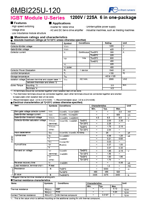
6MBI225U-1201200V / 225A 6 in one-packageFeatures· High speed switching· Voltage drive· Low inductance module structureApplications · Inverter for Motor drive· AC and DC Servo drive amplifierMaximum ratings and characteristicsThermal resistance characteristicsThermal resistanceContact Thermal resistance––0.12––0.20–0.0167 –IGBTFWDWith thermal compound°C/W°C/W°C/W*2 : Two thermistor terminals should be connected together, each other terminals should be connected together and shortedto base plate when isolation test will be done.*3 :Recommendable value : 2.5 to 3.5 N·m(M5) *4 :Recommendable value : 3.5 to 4.5 N·m(M6)Rth(j-c)Rth(j-c)Rth(c-f)*5IGBT Module U-Series*5 : This is the value which is defined mounting on the additional cooling fin with thermal compound.4Items Symbols Conditions Characteristics UnitMin.Typ. Max.· Uninterruptible power supply· Industrial machines, such as Welding machinesCharacteristics (Representative)VGE=0V, f= 1MHz, Tj= 25°CVcc=600V, I=225A, Tj= 25°CCollector current vs. Collector-Emitter voltage (typ.)Tj= 125°C / chipCapacitance vs. Collector-Emitter voltage (typ.)Dynamic Gate charge (typ.)Collector current vs. Collector-Emitter voltage (typ.)Tj= 25°C / chipCollector current vs. Collector-Emitter voltage (typ.)VGE=15V / chipTj=25°C / chipCollector-Emitter voltage vs. Gate-Emitter voltage (typ.)010020030040050060012345C o l l e c t o r c u r r e n t : I c [A ]VGE=20V15V12V10V8V010020030040050060012345C o l l e c t o r c u r r e n t : I c [A ]VGE=20V 15V12V10V8V010020030040050060001234C o l l e c t o r c u r r e n t : I c [A ]Tj=125°CTj=25°C246810510152025C o l l e c t o r - E m i t t e r v o l t a g e : V C E [ V ]Ic=450A Ic=225A Ic= 112.5A0.11.010.0100.0102030C a p a c i t a n c e : C i e s , C o e s , C r e s [ n F ]200400600800100012001400C o l l e c t o r -E m i t t e r v o l t a g e : V C E [ 200V /d i v ]G a t e - E m i t t e r v o l t a g e : V G E [ 5V /d i v]Vcc=600V, Ic=225A, VGE=±15V, Tj= 25°CStray inductance <= 100nHSwitching loss vs. Collector current (typ.)Vcc=600V, VGE=±15V, Rg=3ΩVcc=600V, Ic=225A, VGE=±15V, Tj= 125°C+VGE=15V,-VGE <= 15V, RG >= 3Ω ,Tj <= 125°CSwitching time vs. Collector current (typ.)Vcc=600V, VGE=±15V, Rg=3Ω, Tj=125°CSwitching time vs. Gate resistance (typ.)Switching time vs. Collector current (typ.)Vcc=600V, VGE=±15V, Rg=3Ω, Tj= 25°CReverse bias safe operating area (max.)Switching loss vs. Gate resistance (typ.)10100100010000100200300400S w i t c h i n g t i m e : t o n , t r , t o f f , t f [ n s e c ]Collector current : Ic [ A ]10100100010000100200300400S w i t c h i n g t i m e : t o n , t r , t o f f , t f [ n s e c ]Collector current : Ic [ A ]10100100010000110100S w i t c h i n g t i m e : t o n , t r , t o f f , t f [ n s e c ]Gate resistance : Rg [ Ω ]trtftoffton 01020304050100200300400500S w i t c h i n g l o s s : E o n , E o f f , E r r [ m J /p u l s e ]Collector current : Ic [ A ]Eon(125°C)Eon(25°C)Eoff(125°C)Err(125°C)Err(25°C)Eoff(25°C)0255075100125150110100S w i t c h i n g l o s s : E o n , E o f f , E r r [ m J /p u l s e ]Gate resistance : Rg [ Ω ]EoffErrEon0100200300400500600200400600800100012001400C o l l e c t o r c u r r e n t : I c [ A ]Collector - Emitter voltage : VCE [ V ]Transient thermal resistance (max.)Reverse recovery characteristics (typ.)Vcc=600V, VGE=±15V, Rg=3ΩForward current vs. Forward on voltage (typ.)chipTemperature characteristic (typ.)01002003004005006001234F o r w a r d c u r r e n t : I F [ A ]Forward on voltage : VF [ V ]Tj=125°CTj=25°C101001000100200300400500R e v e r s e r e c o v e r y c u r r e n t : I r r [ A ]R e v e r s e r e c o v e r y t i m e : t r r [ n s e c ]Forward current : IF [ A ]Irr (125°C)Irr (25°C)trr (125°C)trr (25°C)0.0010.0100.1001.0000.0010.0100.1001.000T h e r m a l r e s i s t a n s e : R t h (j -c ) [ °C /W ]Pulse width : Pw [ sec ]0.1110100-60-40-20020406080100120140160180Temperature [°C ]R e s i s t a n c e : R [ k Ω ]Outline Drawings, mmM6296MBI225U-120IGBT ModuleEquivalent Circuit Schematic[Thermister]135111210987246[Inverter]。
- 1、下载文档前请自行甄别文档内容的完整性,平台不提供额外的编辑、内容补充、找答案等附加服务。
- 2、"仅部分预览"的文档,不可在线预览部分如存在完整性等问题,可反馈申请退款(可完整预览的文档不适用该条件!)。
- 3、如文档侵犯您的权益,请联系客服反馈,我们会尽快为您处理(人工客服工作时间:9:00-18:30)。
元器件交易网
Marketing division, Marketing planning department
6-41 Tsukuba, Isahaya, Nagasaki, 854-0065 Japan
Keep safety first in your circuit designs! ·ISAHAYA Electronics Corporation puts the maximum effort into making semiconductor products better and more reliable, but there is always the possibility that trouble may occur with them. Trouble with semiconductors may lead to personal injury, fire or property damage. Remember to give due consideration to safety when making your circuit designs, with appropriate measures such as (1) placement of substitutive, auxiliary, (2) use of non-farmable material or (3) prevention against any malfunction or mishap. Notes regarding these materials ·These materials are intended as a reference to our customers in the selection of the ISAHAYA products best suited to the customer’s application; they don't convey any license under any intellectual property rights, or any other rights, belonging ISAHAYA or third party. ·ISAHAYA Electronics Corporation assumes no responsibility for any damage, or infringement of any third party's rights , originating in the use of any product data, diagrams, charts or circuit application examples contained in these materials. ·All information contained in these materials, including product data, diagrams and charts, represent information on products at the time of publication of these materials, and are subject to change by ISAHAYA Electronics Corporation without notice due to product improvements or other reasons. It is therefore recommended that customers contact ISAHAYA Electronics Corporation or an authorized ISAHAYA products distributor for the latest product information before purchasing product listed herein. ·ISAHAYA Electronics Corporation products are not designed or manufactured for use in a device or system that is used under circumstances in which human life is potentially at stake. Please contact ISAHAYA electronics corporation or an authorized ISAHAYA products distributor when considering the use of a product contained herein for any specific purposes , such as apparatus or systems for transportation, vehicular, medical, aerospace, nuclear, or undersea repeater use. ·The prior written approval of ISAHAYA Electronics Corporation is necessary to reprint or reproduce in whole or in part these materials. ·If these products or technologies are subject to the Japanese export control restrictions, they must be exported under a license from the Japanese government and cannot be imported into a country other than the approved destination. Any diversion or re-export contrary to t e export control laws and regulations of Japan and/or the country of destination is h prohibited. ·Please contact ISAHAYA Electronics Corporation or authorized ISAHAYA products distributor for further details on these materials or the products contained therein.
1
INPUT OFF VOLTAGE VI(OFF) (V)
ISAHAYA ELECTRONICS CORPORATION
元器件交易网
RT2N62M
Composite Transistor For Muting Application Silicon NPN Epitaxial Type
DC FORWARD CURRENT GAIN VS. COLLECTOR CURRENT 10000 10000
DC REVERSE CURRENT GAIN VS. COLLECTOR CURRENT
DC FORWARD CURRENT GAIN hFE
1000
DC REVERSE CURRENT GAIN hFER
PC Tj Tstg
N62
ISAHAYA ELECTRONICS CORPORATION
元器件交易网
RT2N62M
Composite Transistor For Muting Application Silicon NPN Epitaxial Type
Electrical characteristics(Ta=25℃)
Limits Min 40 40 20 0.5 0.5 820 10 1.54 2.2 40 0.70 2.86 2500 Typ Max
Unit V V V μA μA mV KΩ MHz Ω
V I=5V, f=1MHz
Байду номын сангаас
TYPICAL CHARACTERISTICS (Tr1、Tr2)
INPUT ON VOLTAGE VS. COLLECTOR CURRENT 100 Ta=25℃ VCE=0.2V INPUT ON VOLTAGE VI(ON) (V)
COLLECTOR CURRENT VS. INPUT OFF VOLTAGE 1000 Ta=25℃ VCE=5V
10
COLLECTOR CURRENT IC (μA)
100
1
10
0.1 0.1 1 10 COLLECTOR CURRENT IC (mA) 100 1000
0
0.2
0.4
0.6
0.8
元器件交易网
RT2N62M
Composite Transistor For Muting Application Silicon NPN Epitaxial Type
OUTLINE DRAWING DESCRIPTION
RT2N62M is a composite transistor with built-in bias resistor ① 2.1 1.25 ⑤ 0.2 0.13 ④ RTr2 0~0.1 R1 ② ③
MARKING
⑤ ④
Collector to Base voltage Emitter to Base voltage Collector to Emitter voltage Collector current Collector dissipation(Total Ta=25℃) Junction temperature Storage temperature
R1 ①
TERMINAL CONNECTOR ①:BASE1 ②:EMITTER(COMMON) ③:BASE2 ④:COLLECTOR2 ⑤:COLLECTOR1 JEITA:- JEDEC:-