MAX3935中文资料
MAX391CPE中文资料

MAX391/MAX392/MAX393Precision, Quad, SPST Analog Switches________________________________________________________________Maxim Integrated Products 1_____________________Pin Configurations/Functional Diagrams/Truth Tables19-0236; Rev 3; 8/06Ordering Information continued on last page.*Contact factory for dice specifications.†EP = Exposed pad.Ordering Information_______________General DescriptionThe MAX391/MAX392/MAX393 are precision, quad,single-pole/single-throw (SPST) analog switches designed to operate at +3V, +5V, or ±5V. The MAX391has four normally closed (NC) switches, and the MAX392 has four normally open (NO) switches. The MAX393 has two NO and two NC switches. All three devices offer low leakage (100pA max) and fast switch-ing speeds (t ON ≤130ns, t OFF ≤75ns). Power con-sumption is just 1µW—ideal for battery-operated equip-ment. All devices operate from a single +3V to +15V supply or from dual ±3.0V to ±8V supplies.With ±5V supplies, the MAX391/MAX392/MAX393 offer guaranteed 2Ωmax channel-to-channel matching, 30Ωmax on-resistance (R ON ), and 4Ωmax R ON flatness over the specified range.These switches are also fully specified for single +5V operation, with 2Ωmax R ON match, 60Ωmax R ON, and 6Ωmax flatness.These low-voltage switches also offer 5pC max charge injection, and ESD protection is greater than 2000V, per method 3015.7.________________________ApplicationsBattery-Operated Systems Sample-and-Hold Circuits Heads-Up Displays Guidance and Control Systems Audio and Video Switching Military RadiosTest Equipment Communications Systems ±5V DACs and ADCsPBX, PABX____________________________Features♦Low On-Resistance, 20ΩTypical♦Guaranteed On-Resistance Match Between Channels, < 2Ω♦Guaranteed On-Resistance Flatness Over Signal Range, 4ΩMax♦Guaranteed Charge Injection, < 5pC ♦Improved Leakage Over Temperature,< 2.5nA at +85°C♦Electrostatic Discharge > 2000V per Method 3015.7♦Single-Supply Operation (+3V to +15V)Bipolar-Supply Operation (±3V to ±8V)♦Low Power Consumption, < 1µW ♦TTL/CMOS-Logic CompatibleFor pricing, delivery, and ordering information, please contact Maxim Direct at 1-888-629-4642,or visit Maxim's website at .M A X 391/M A X 392/M A X 393Precision, Quad, SPST Analog SwitchesVoltage Referenced to V-V+.......................................................................-0.3V to +17V GND....................................................................-0.3V to +17V GND..........................................................-0.3V to (V+ + 0.3V)V IN_, V COM_, V NC_, V NO_(Note 1)..................................V- to V+Current (any terminal).........................................................30mA Peak Current, COM_, NO_, NC_(pulsed at 1ms, 10% duty cycle max)..........................100mA ESD per Method 3015.7.................................................> 2000V Continuous Power Dissipation (T A = +70°C)Plastic DIP (derate 10.53mW/°C above+70°C)...........842mW Narrow SO (derate 8.70mW/°C above +70°C)............696mW TSSOP (derate 6.7mW/°C above +70°C)....................457mW CERDIP (derate 10.00mW/°C above +70°C)...............800mW QFN (derate 18.5mW/°C above +70°C)....................1481mW Operating Temperature RangesMAX39_C_ _.......................................................0°C to +70°C MAX39_E_ _.....................................................-40°C to +85°C MAX39_M_ _..................................................-55°C to +125°C Storage Temperature Range.............................-65°C to +150°C Lead Temperature (soldering, 10s).................................+300°CELECTRICAL CHARACTERISTICS—Dual Supplies(V+ = +5V ±10%, V- = -5V ±10%, GND = 0V, V INH = 2.4V, V INL = 0.8V, T A = T MIN to T MAX , unless otherwise noted.)Stresses beyond those listed under “Absolute Maximum Ratings” may cause permanent damage to the device. These are stress ratings only, and functional operation of the device at these or any other conditions beyond those indicated in the operational sections of the specifications is not implied. Exposure to absolute maximum rating conditions for extended periods may affect device reliability.Note 1:Signals on NC_, NO_, COM_, or IN_ exceeding V+ or V- are clamped by internal diodes. Limit forward diode current to maxi-mum current rating.ABSOLUTE MAXIMUM RATINGSMAX391/MAX392/MAX393Precision, Quad, SPST Analog Switches_______________________________________________________________________________________3ELECTRICAL CHARACTERISTICS—Dual Supplies (continued)(V+ = +5V ±10%, V- = -5V ±10%, GND = 0V, V INH = 2.4V, V INL = 0.8V, T A = T MIN to T MAX , unless otherwise noted.)M A X 391/M A X 392/M A X 393Precision, Quad, SPST Analog Switches 4_______________________________________________________________________________________ELECTRICAL CHARACTERISTICS—Single +5V Supply(V+ = +5V ±10%, V- = 0V ±10%, GND = 0V, V INH = 2.4V, V INL = 0.8V, T A = T MIN to T MAX , unless otherwise noted.)MAX391/MAX392/MAX393Precision, Quad, SPST Analog Switches_______________________________________________________________________________________5ELECTRICAL CHARACTERISTICS—Single +3.3V Supply(V+ = +3.0V to +3.6V, GND = 0V, V INH = 2.4V, V INL = 0.8V, T A = T MIN to T MAX , unless otherwise noted.)Note 2:The algebraic convention, where the most negative value is a minimum and the most positive value a maximum, is used in this data sheet.Note 3:Guaranteed by design.Note 4:ΔR ON = ΔR ON max - ΔR ON min.Note 5:Flatness is defined as the difference between the maximum and minimum value of on-resistance as measured over the specified analog signal range.Note 6:Leakage parameters are 100% tested at maximum rated hot temperature and guaranteed by correlation at +25°C.Note 7:Off-isolation = 20 log 10[ V COM_⁄ (V NC_ or V NO_)], V COM_= output, V NC_ or V NO_= input to off switch.Note 8:Between any two switches.Note 9:Leakage testing at single supply is guaranteed by testing with dual singles.M A X 391/M A X 392/M A X 393Precision, Quad, SPST Analog Switches 6_________________________________________________________________________________________________________________________________Typical Operating Characteristics(T A = +25°C, unless otherwise noted.)10001000.01-4085FORWARD SHUTDOWN CURRENTvs. TEMPERATURE0.1110TEMPERATURE (°C)F O R W A R D S H U T D O W N C U R R E N T (n A )603510-1510-5.0-2.52.5R ON vs. V COM ANDTEMPERATURE (DUAL SUPPLIES)35V COM (V)R O N (Ω)0 5.0251530204048R ON vs. V COM (SINGLE SUPPLY)100V COM (V)R O N (Ω)6106020804012012213R ON vs. V COM ANDTEMPERATURE (SINGLE SUPPLY)100V COM (V)R O N (Ω)24602080401205-30-5.0CHARGE INJECTION vs. V COM20V COM (V)Q (p C)0 5.00-2010-1030-2.52.50.0001-75OFF-LEAKAGE CURRENT vs.TEMPERATURE10TEMPERATURE (°C)O F F L E A K A G E (n A )251250.10.00110.01100-25750.0001-75ON-LEAKAGE CURRENT vs.TEMPERATURE10TEMPERATURE (°C)O N L E A K AG E (n A )251250.10.00110.01100-25750.0001-75SUPPLY CURRENT vs. TEMPERATURE10TEMPERATURE (°C)I +, I -, (μA )251250.10.00110.01100MAX391/MAX392/MAX393Precision, Quad, SPST Analog Switches_______________________________________________________________________________________7__________Applications InformationOvervoltage ProtectionProper power-supply sequencing is recommended for all CMOS devices. Do not exceed the absolute maxi-mum ratings, because stresses beyond the listed rat-ings may cause permanent damage to the devices.Always sequence V+ on first, followed by V-, and then logic inputs. If power-supply sequencing is not possi-ble, add two small signal diodes in series with supply pins for overvoltage protection (Figure 1). Adding diodes reduces the analog signal range to 1V below V+and 1V below V-, but low switch resistance and low leakage characteristics are unaffected. Device opera-tion is unchanged, and the difference between V+ and V- should not exceed 17V.DiodesM A X 391/M A X 392/M A X 393Precision, Quad, SPST Analog Switches 8_______________________________________________________________________________________Figure 4. Charge InjectionFigure 2. Switching TimeFigure 3. Break-Before-Make Interval (MAX393 only)______________________________________________Test Circuits/Timing DiagramsMAX391/MAX392/MAX393Precision, Quad, SPST Analog Switches_______________________________________________________________________________________9Figure 6. CrosstalkFigure 5. Off-Isolation_________________________________Test Circuits/Timing Diagrams (continued)Figure 8. Channel On-CapacitanceFigure 7. Channel Off-CapacitanceM A X 391/M A X 392/M A X 393Precision, Quad, SPST Analog Switches 10________________________________________________________________________________________Ordering Information (continued)___________________Chip TopographyCOM30.067"(1.70mm)IN4IN3 "C""B"COM4TRANSISTOR COUNT: 76SUBSTRATE CONNECTED TO V+MAX391MAX392MAX393PIN NAME NAME PIN PIN *Contact factory for dice specifications.**Contact factory for availability and processing to MIL-STD-883.†EP = Exposed pad.MAX391/MAX392/MAX393Precision, Quad, SPST Analog SwitchesPackage Information(The package drawing(s) in this data sheet may not reflect the most current specifications. For the latest package outline information go to /packages .)Pin Configurations/Functional Diagrams/Truth Tables (continued)M A X 391/M A X 392/M A X 393Precision, Quad, SPST Analog SwitchesPackage Information (continued)(The package drawing(s) in this data sheet may not reflect the most current specifications. For the latest package outline information go to /packages .)MAX391/MAX392/MAX393Precision, Quad, SPST Analog SwitchesMaxim cannot assume responsibility for use of any circuitry other than circuitry entirely embodied in a Maxim product. No circuit patent licenses are implied. Maxim reserves the right to change the circuitry and specifications without notice at any time.13__________________Maxim Integrated Products, 120 San Gabriel Drive, Sunnyvale, CA 94086 (408) 737-7600©2006 Maxim Integrated Productsis a registered trademark of Maxim Integrated Products, Inc.Package Information (continued)(The package drawing(s) in this data sheet may not reflect the most current specifications. For the latest package outline information go to /packages .)Revision HistoryPages changed at Rev 3: 1–11, 13。
MAX2335中文资料
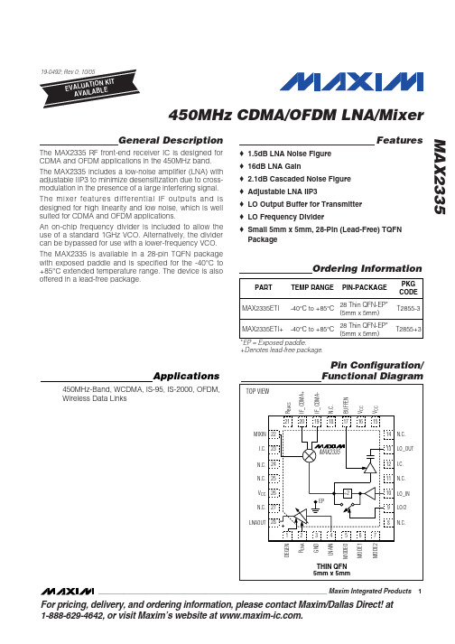
Ordering Information
PART
TEMP RANGE PIN-PACKAGE
PKG CODE
MAX2335ETI
-40°C to +85°C
28 Thin QFN-EP* (5mm x 5mm)
T2855-3
MAX2335ETI+ -40°C to +85°C
*EP = Exposed paddle. +Denotes lead-free package.
28-Pin Thin QFN (derate 34.5mW/°C above +70°C) ...........2.7W
Operating Temperature Range ...........................-40°C to +85°C Junction Temperature ......................................................+150°C Storage Temperature Range .............................-65°C to +150°C Lead Temperature (soldering, 10s) .................................+300°C
元器件交易网
MAX2335
450MHz CDMA/OFDM LNA/Mixer
ABSOLUTE MAXIMUM RATINGS
VCC to GND ...........................................................-0.3V to +4.3V All Other Pins to GND.................................-0.3V to (VCC + 0.3V) AC Input Pins (LNAIN, LO_IN, MIXIN) to GND ...............1V Peak Continuous Power Dissipation (TA = +70°C)
max3485esa中文资料
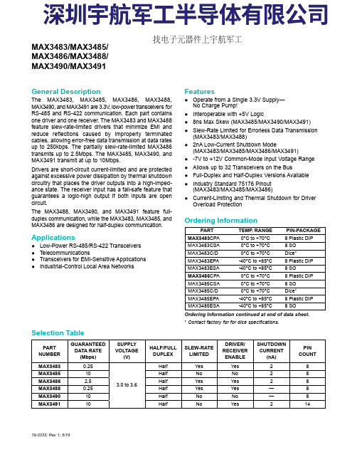
General Description The MAX3483, MAX3485, MAX3486, MAX3488,MAX3490, and MAX3491 are 3.3V , low-power transceivers forRS-485 and RS-422 communication. Each part containsone driver and one receiver. The MAX3483 and MAX3488feature slew-rate-limited drivers that minimize EMI andreduce reflections caused by improperly terminatedcables, allowing error-free data transmission at data ratesup to 250kbps. The partially slew-rate-limited MAX3486transmits up to 2.5Mbps. The MAX3485, MAX3490, andMAX3491 transmit at up to 10Mbps.Drivers are short-circuit current-limited and are protectedagainst excessive power dissipation by thermal shutdowncircuitry that places the driver outputs into a high-imped-ance state. The receiver input has a fail-safe feature thatguarantees a logic-high output if both inputs are opencircuit.The MAX3488, MAX3490, and MAX3491 feature full-duplex communication, while the MAX3483, MAX3485, andMAX3486 are designed for half-duplex communication.Applications ●Low-Power RS-485/RS-422 Transceivers ●Telecommunications ●Transceivers for EMI-Sensitive Applications ●Industrial-Control Local Area NetworksFeatures●Operate from a Single 3.3V Supply—No Charge Pump!●Interoperable with +5V Logic ●8ns Max Skew (MAX3485/MAX3490/MAX3491)●Slew-Rate Limited for Errorless Data Transmission (MAX3483/MAX3488)●2nA Low-Current Shutdown Mode (MAX3483/MAX3485/MAX3486/MAX3491)●-7V to +12V Common-Mode Input Voltage Range ●Allows up to 32 Transceivers on the Bus ●Full-Duplex and Half-Duplex Versions Available ●Industry Standard 75176 Pinout (MAX3483/MAX3485/MAX3486)●Current-Limiting and Thermal Shutdown for Driver Overload Protection 19-0333; Rev 1; 5/19Ordering Information continued at end of data sheet.*Contact factory for for dice specifications.PARTTEMP . RANGE PIN-PACKAGE MAX3483CPA0°C to +70°C 8 Plastic DIP MAX3483CSA0°C to +70°C 8 SO MAX3483C/D0°C to +70°C Dice*MAX3483EPA-40°C to +85°C 8 Plastic DIP MAX3483ESA-40°C to +85°C 8 SO MAX3485CPA0°C to +70°C 8 Plastic DIP MAX3485CSA0°C to +70°C 8 SO MAX3485C/D0°C to +70°C Dice*MAX3485EPA-40°C to +85°C 8 Plastic DIP MAX3485ESA -40°C to +85°C 8 SO PARTNUMBERGUARANTEED DATA RATE (Mbps)SUPPLY VOLTAGE (V)HALF/FULL DUPLEX SLEW-RATE LIMITED DRIVER/RECEIVER ENABLE SHUTDOWN CURRENT (nA)PIN COUNT MAX34830.25 3.0 to 3.6Half Yes Yes 28MAX348510Half No No 28MAX34862.5Half Yes Yes 28MAX34880.25Half Yes Yes —8MAX349010Half No No —8MAX349110Half No Yes 214MAX3483/MAX3485/MAX3486/MAX3488/MAX3490/MAX3491Selection TableOrdering Information找电子元器件上宇航军工Figure 1. MAX3483/MAX3485/MAX3486 Pin Configuration and Typical Operating Circuit Figure 2. MAX3488/MAX3490 Pin Configuration and Typical Operating Circuit Figure 3. MAX3491 Pin Configuration and Typical Operating CircuitMAX3486/MAX3488/MAX3490/MAX3491True RS-485/RS-422 TransceiversFigure 22. MAX3488/MAX3490/MAX3491 Full-Duplex RS-485 NetworkFigure 23. Line Repeater for MAX3488/MAX3490/MAX3491MAX3486/MAX3488/MAX3490/MAX3491True RS-485/RS-422 Transceivers。
MAX5435LEZT-T中文资料

R (kΩ) 50 50 100 100 50
PKG CODE T833-1 T833-1 T833-1 T833-1 Z6-1
________________________________________________________________ Maxim Integrated Products 1
The MAX5432–MAX5435 feature an internal, nonvolatile, electrically erasable programmable read-only memory (EEPROM) that returns the wiper to its previously stored position at power-up. The fast-mode I2C-compatible serial interface allows communication at data rates up to 400kbps, minimizing board space and reducing interconnection complexity. Each device is available with multiple factory-preset I2C addresses (see the Ordering Information/Selector Guide).
MAX5432–MAX5435
32-Tap, Nonvolatile, I2C, Linear, Digital Potentiometers
ABSOLUTE MAXIMUM RATINGS
LM39300-5.0资料

APPLICATIONS•LDO linear regulator for PC add-in cards •High-efficiency linear power supplies •Multimedia and PC processor supplies •SMPS post regulator•Low-voltage microcontrollers •StrongARM™ processor supplyORDERING INFORMATIONDESCRIPTIONHTCLM39302T-Adj LM39302-Adj LM39300T-X.X TO-220LM39301T-X.X TO-220Regulator OutputADJOUT Device Marking Flag (Output): Open-collector error flag output.LM39301R-X.X TO-263LM39301-X.X TO-263LM39300-X.X LM39300R- X.X LM39301-X.X LM39302R-Adj TO-220GND FLG Ground pin and TAB are internally connected.LM39300-X.X Adjustment Input: Feedback input.Package LM39302-Adj TO-263PIN DESCRIPTIONEnable (Input)IN CMOS-compatible control input.Logic high = enable, logic Logic low or open = Shutdown Supply (Input): +16V maximum supply * X.X = Fixed Vout = 1.5V, 1.8V, 2.5V, 3.3V, 5.0VThe LM39300/1/2 is ideal for PC add-in cards that need to convert from standard 5V or 3.3V down to new,lower core voltages. A guaranteed maximum dropout voltage of 500mV over all operating conditions allows the LM39300/1/2 to pro-vide 2.5V from a supply as low as 3V.The LM39300/1/2 also has fast transient response for heavy switching applications.The device requires only 47F of output capacitance to maintain stability and achieve fast transient responseThe LM39300/1 is fully protected with over current limiting,thermal shutdown, reversed-battery protection, reversed-leakage protection, and reversed-lead insertion. The LM39301 offers a TTL-logic compatible enable pin and an error flag that indicates under voltage and over current conditions. Offered in fixed voltages, theLM39300/1/2 comesin the TO-220 and TO-263 packages and is an ideal upgrade to older, NPN-based linear voltage regulators.TO263-3L / TO220-3LTO263-5L / TL220-5L(39301-x.x & 39302 only)The LM39300, LM39301 and LM39302 are 3.0A low-dropout linear voltage regulators that provide a low voltage, high-current output with a minimum of external components.The LM39300/1 offers extremely low dropout (typically 400mV at 3.0A) and low ground current (typically 36mA at 3.0A).Typical Application CircuitAbsolute Maximum Ratings (Note 1)Supply Voltage (VIN) : –20V to +20V Enable Voltage (VEN) : +20VStorage Temperature (TS) : –65°C to +150°C Lead Temperature (soldering, 5 sec) : 260°C ESD, Note 3Operating Ratings (Note 2)Supply Voltage (VIN) : +2.25V to +16V Enable Voltage (VEN) : +16VMaximum Power Dissipation (PD(max)) Note 4 Junction Temperature (TJ) : –40°C to +125°C Package Thermal Resistance TO-263(θJC) : 2°C/WTO-220(θJC) : 2°C/WLM39300LM39301LM39302Block DiagramLM39300 Fixed (1.5V,1.8V,2.5V,3.3V,5.0V)LM39301 Fixed with Flag and EnableLM39302 Adjustable550Note 1. Exceeding the absolute maximum ratings may damage the device.Note 2. The device is not guaranteed to function outside its operating rating.Note 3. Devices are ESD sensitive. Handling precautions recommended.Note 4. P D(max) = (T J(max) – T A) θJA, where θJA depends upon the printed circuit layout. See “Applications Information.”Note 5.Vout temperature coefficient is ∆V OUT(worst case) (T J(max) – T J(min)) where T J(max) is +125℃ and T J(min) is 0℃Note 6. V DO = V IN – V OUT when V OUT decreases to 99% of its nominal output voltage with V IN = V OUT + 1V.Note 7. I GND is the quiescent current. IIN = I GND + I OUT.Note 8. V EN 0.8V, V IN 8V, and V OUT = 0VNote 9. For a 2.5V device, V IN = 2.250V (device is in dropout).Note 10.VREF ≤ VOUT ≤ (VIN – 1V), 2.25V ≤ VIN ≤ 16V, 10mA ≤ IL ≤ 1A, TJ = TMAX.TYPICAL PERFORMANCE CHARACTERISTICSAPPLICATION INFORMATIONThe LM39300/1 is a high-performance low-dropout voltage regulator suitable for moderate to high-current voltage regu-lator applications. Its 500mV dropout voltage at full load makes it especially valuable in battery-powered systems and as a high-efficiency noise filter in post-regulator applications. Unlike older NPN-pass transistor designs, where the mini-mum dropout voltage is limited by the base-to-emitter voltage drop and collector-to-emitter saturation voltage, dropout per-formance of the PNP output of these devices is limited only by the low V CE saturation voltage.A trade-off for the low dropout voltage is a varying base drive requirement. The LM39300/1/2 regulator is fully protected from damage due to fault conditions. Current limiting is provided. This limiting is linear output current during overload conditions is constant. Thermal shutdown disables the device when the die temperature exceeds the maximum safe operating tem-perature. Transient protection allows device (and load) sur-vival even when the input voltage spikes above and below nominal. The output structure of these regulators allows voltages in excess of the desired output voltage to be applied without reverse current flow.Thermal DesignLinear regulators are simple to use. The most complicated design parameters to consider are thermal characteristics.Thermal design requires four application-specific param-eters:•Maximum ambient temperature (T A)•Output Current (I OUT)•Output Voltage (V OUT)•Input Voltage (V IN)•Ground Current (I GND)Calculate the power dissipation of the regulator from these numbers and the device parameters from this datasheet,where the ground current is taken from the data sheet.PD = (V IN – V OUT) I OUT + V IN·I GNDThe heat sink thermal resistance is determined by:θSA=(T JMAX-T A)/P D -(θJC+θCS)where TJ (max) 125 ℃ and θCS is between 0℃ and 2℃/W.The heat sink may be significantly reduced in applications where the minimum input voltage is known and is large compared with the dropout voltage. Use a series input resistor to drop excessive voltage and distribute the heat between this resistor and the regulator. The low dropout properties of Taejin regulators allow signifi-cant reductions in regulator power dissipation and the asso-ciated heat sink without compromising performance. When this technique is employed, a capacitor of at least 1.0F is needed directly between the input and regulator ground.Refer to Application Note 9 for further details and examples on thermal design and heat sink specification.Output CapacitorThe LM39300/1/2 requires an output capacitor to maintain stability and improve transient response. Proper capacitor selection is important to ensure proper operation. The LM39300/1/2 output capacitor selection is dependent upon the ESR (equivalent series resistance) of the output capacitor to maintain stability. When the output capacitor is 47F or greater, the output capacitor should have less than 1 of ESR. This will improve transient response as well as promote stability. Ultralow ESR capacitors, such as ceramic chip capacitors may promote instability. These very low ESR levels may cause an oscillation and/or underdamped tran-sient response. A low-ESR solid tantalum capacitor works extremely well and provides good transient response and stability over temperature. Aluminum electrolytics can also be used, as long as the ESR of the capacitor is < 1.The value of the output capacitor can be increased without limit. Higher capacitance values help to improve transient response and ripple rejection and reduce output noise. Input CapacitorAn input capacitor of 1F or greater is recommended when the device is more than 4 inches away from the bulk ac supply capacitance, or when the supply is a battery. Small, surface-mount, ceramic chip capacitors can be used for the bypass-ing. Larger values will help to improve ripple rejection by bypassing the input to the regulator, further improving the integrity of the output voltage.Transient Response and 3.3V.Fig 1. Capacitor RequirementsMinimum Load CurrentThe LM39300/1/2 regulator is specified between finite loads.If the output current is too small, leakage currents dominate and the output voltage rises.A 10mA minimum load current is necessary for proper regulation.Transient Response and 3.3V to 2.5V ConversionThe LM39300/1/2 has excellent transient response to varia-tions in input voltage and load current. The device has been designed to respond quickly to load current variations and input voltage variations. Large output capacitors are not required to obtain this performance. A standard 47F output capacitor, preferably tantalum, is all that is required. Larger values help to improve performance even further.By virtue of its low-dropout voltage, this device does not saturate into dropout as readily as similar NPN-based de-signs. When converting from 3.3V to 2.5V, the NPN-based regulators are already operating in dropout, with typical dropout requirements of 1.2V or greater. To convert down to 2.5V without operating in dropout, NPN-based regulators require an input voltage of 3.7V at the very least. TheLM39300/1/2 regulator will provide excellent performance with an input as low as 3.0V. This gives the PNP-based regulators a distinct advantage over older, NPN-based linear regulators.Error FlagThe LM39301 version features an error flag circuit which monitors the output voltage and signals an error condition when the voltage drops 5% below the nominal output voltage. The error flag is an open-collector output that can sink 10mA during a fault condition.Low output voltage can be caused by a number of problems, including an overcurrent fault (device in current limit) or low input voltage. The flag is inoperative during overtemperature shutdown.Enable InputThe LM39301 version features an enable input for on/off control of the device. Its shutdown state draws “zero” current (only microamperes of leakage). The enable input is TTL/ CMOS compatible for simple logic interface, but can be connected to up to 20V. When enabled, it draws approxi-mately 15A.Adjustable Regulator DesignThe LM39302 allows programming the output voltage any-where between 1.25V and the 16V maximum operating rating of the family. Two resistors are used. Resistors can be quite large, up to 1MΩ, because of the very high input impedance and low bias current of the sense comparator: The resistor values are calculated by :R1=R2(Vout/1.250-1)Where VO is the desired output voltage. Figure 1 shows component definition. Applications with widely varying load currents may scale the resistors to draw the minimum load current required for proper operation (see below).。
MAX2605-MAX2609中文资料
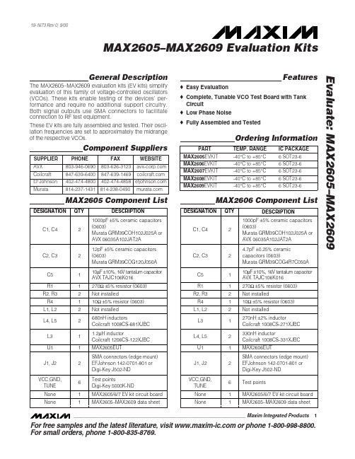
General DescriptionThe MAX2605–MAX2609 evaluation kits (EV kits) simplify evaluation of this family of voltage-controlled oscillators (VCOs). These kits enable testing of the devices’ per-formance and require no additional support circuitry.Both signal outputs use SMA connectors to facilitate connection to RF test equipment.These EV kits are fully assembled and tested. Their oscil-lation frequencies are set to approximately the midrange of the respective VCOs.Featureso Easy Evaluationo Complete, Tunable VCO Test Board with Tank Circuit o Low Phase Noiseo Fully Assembled and TestedEvaluate: MAX2605–MAX2609MAX2605–MAX2609 Evaluation Kits19-1673 Rev 0; 9/00Ordering InformationComponent SuppliersFor free samples and the latest literature, visit or phone 1-800-998-8800.For small orders, phone 1-800-835-8769.MAX2606 Component ListMAX2605 Component ListE v a l u a t e : M A X 2605–M A X 2609MAX2605–MAX2609 Evaluation Kits 2_______________________________________________________________________________________Quick StartThe MAX2605–MAX2609 evaluation kits are fully assembled and factory tested. Follow the instructions in the Connections a nd Setup section for proper device evaluation.Test Equipment Required•Low-noise power supplies (these are recommended for oscillator noise measurement). Noise or ripple will frequency-modulate the oscillator and cause spectral spreading. Batteries can be used in place of power supplies, if necessary.– Use a DC power supply capable of supplying +2.7V to +5.5V. Alternatively, use two or three 1.5V batteries.– Use a DC power supply capable of supplying +0.4V to +2.4V, continuously variable, for TUNE.Alternatively, use two 1.5V batteries with a resistive voltage divider or potentiometer.•An RF spectrum analyzer that covers the operating frequency range of the MAX2605–MAX2609• A 50Ωcoaxial cable with SMA connectors •An ammeter (optional)Connections and Setup1)Connect a DC supply (preset to +3V) to the V CC and GND terminals (through an ammeter, if desired) on the EV kit.2)Turn on the DC supply. If used, the ammeter readingMAX2607 Component ListMAX2608 Component ListEvaluate: MAX2605–MAX2609MAX2605–MAX2609 Evaluation Kits_______________________________________________________________________________________3approximates the typical operating current specified in the MAX2605–MAX2609 data sheet.3)Connect the VCO output (OUT+ or OUT-) to a spec-trum analyzer with a 50Ωcoaxial cable.4)Apply a positive variable DC voltage between 0.4V and 2.4V to TUNE.5)Check the tuning bandwidth on the spectrum analyz-er by varying the tuning voltage (+0.4V to +2.4V).Layout ConsiderationsThe EV kit PC board can serve as a guide for laying out a board using the MAX2605–MAX2609. Generally, the VCC pin on the PC board should have a decoupling capacitor placed close to the IC. This minimizes noisecoupling from the supply. Also, place the VCO as far away as possible from the noisy section of a larger sys-tem, such as a switching regulator or digital circuits.The VCO ’s performance is strongly dependent on the availability of the external tuning inductor. For best per-formance, use high-Q components and choose their val-ues carefully. To minimize the effects of parasitic ele-ments, which degrade circuit performance, place the tuning inductor and C BYP close to the VCO. For higher-frequency versions, include the parasitic PC board inductance and capacitance when calculating the oscillation frequency. In addition, remove the ground plane around and under the tuning inductor to minimize the effect of parasitic capacitance.Noise on TUNE translates into FM noise on the outputs;therefore, keep the trace between TUNE and the control circuitry as short as possible. If necessary, use an RC filter to further suppress noise, as done on the EV kits.E v a l u a t e : M A X 2605–M A X 2609MAX2605–MAX2609 Evaluation Kits 4_______________________________________________________________________________________Figure 2. MAX2608/MAX2609 EV Kits SchematicFigure 1. MAX2605/MAX2606/MAX2607 EV Kits SchematicEvaluate: MAX2605–MAX2609MAX2605–MAX2609 Evaluation Kits_______________________________________________________________________________________5Figure 3. MAX2605/MAX2606/MAX2607 EV Kits ComponentPlacement Guide—Top Silk ScreenFigure 4. MAX2608/MAX2609 EV Kits Component PlacementGuide—Top Silk ScreenFigure 5. MAX2605/MAX2606/MAX2607 EV Kits PC BoardLayout—Component SideFigure 6. MAX2608/MAX2609 EV Kits PC Board Layout—Component SideMa xim ca nnot a ssume responsibility for use of a ny circuitry other tha n circuitry entirely embodied in a Ma xim product. No circuit pa tent licenses a re implied. Maxim reserves the right to change the circuitry and specifications without notice at any time.6_____________________Maxim Integrated Products, 120 San Gabriel Drive, Sunnyvale, CA 94086 408-737-7600©2000 Maxim Integrated ProductsPrinted USAis a registered trademark of Maxim Integrated Products.E v a l u a t e : M A X 2605–M A X 2609MAX2605–MAX2609 Evaluation Kits Figure 7. MAX2605/MAX2606/MAX2607/MAX2608/MAX2609EV Kits PC Board Layout—Ground Plane。
MAX8515A-MAX8515中文资料

ELECTRICAL CHARACTERISTICS
(VIN = 3.3V, OUT = FB, IOUT = 5mA, TA = -40°C to +85°C, unless otherwise noted. Typical values are at TA = +25°C.) (Note 1)
PARAMETER IN IN Voltage Range IN Supply Current FB TA = +25°C FB Threshold Accuracy TA = 0°C to +85°C TA = -40°C to +85°C FB Load Regulation FB Line Regulation FB Output Voltage Regulation FB Input Bias Current OUT OUT Voltage Range Maximum Output Current Output Leakage Current Dynamic Output Impedance VOUT IOUT(MAX) VOUT = 0.2V, VIN = 2V, VFB = 0.63V IOUT(LEAK) ZOUT VIN = 28V, VOUT = 18V, VFB = 0V TA = +25°C TA = +85°C 0.2 20 0.001 0.03 0.2 0.32 0.1 18 V mA µA Ω IFB(BIAS) IOUT = 1mA to 20mA VIN = 2V to 28V VIN = 1.7V to 28V VOUT = 0.2V to 18V, IOUT = 1mA VIN = 28V -0.1 0.2 0.02 MAX8515AE_K MAX8515E_K MAX8515AE_K MAX8515E_K MAX8515AE_K MAX8515E_K 0.597 0.594 0.595 0.592 0.594 0.589 0.6 0.6 0.6 0.6 0.6 0.6 3.8 0.2 0.603 0.606 0.605 0.608 0.606 0.608 6 1 1.5 1 +0.1 mV mV mV µA V VIN IIN VIN = 2V to 28V IOUT = 0.3mA IOUT = 10mA 1.7 0.5 2.5 28 1 4 V mA SYMBOL CONDITIONS MIN TYP MAX UNITS
MAX3225EAAP+中文资料

________________General DescriptionThe MAX3224E/MAX3225E/MAX3226E/MAX3227E/MAX3244E/MAX3245E are 3V-powered EIA/TIA-232and V.28/V.24 communications interfaces with automat-ic shutdown/wakeup features, high data-rate capabili-ties, and enhanced electrostatic discharge (ESD)protection. All transmitter outputs and receiver inputs are protected to ±15kV using IEC 1000-4-2 Air-Gap Discharge, ±8kV using IEC 1000-4-2 Contact Discharge,and ±15kV using the Human Body Model.All devices achieve a 1µA supply current using Maxim’s revolutionary AutoShutdown Plus™ feature. These devices automatically enter a low-power shutdown mode when the RS-232 cable is disconnected or the transmitters of the connected peripherals are inactive,and the UART driving the transmitter inputs is inactive for more than 30 seconds. They turn on again when they sense a valid transition at any transmitter or receiv-er input. AutoShutdown Plus saves power without changes to the existing BIOS or operating system.The MAX3225E/MAX3227E/MAX3245E also feature MegaBaud™ operation, guaranteeing 1Mbps for high-speed applications such as communicating with ISDN modems. The MAX3224E/MAX3226E/MAX3244E guar-antee 250kbps operation. The transceivers have a pro-prietary low-dropout transmitter output stage enabling true RS-232 performance from a +3.0V to +5.5V supply with a dual charge pump. The charge pump requires only four small 0.1µF capacitors for operation from a 3.3V supply. The MAX3224E–MAX3227E feature a logic-level output (READY) that asserts when the charge pump is regulating and the device is ready to begin transmitting.All devices are available in a space-saving TQFN,SSOP, and TSSOP (MAX3224E/MAX3225E/MAX3244E/MAX3245E) packages.________________________ApplicationsNotebook, Subnotebook, and Palmtop Computers Cellular PhonesBattery-Powered Equipment Hand-Held Equipment Peripherals Printers__Next Generation Device Features♦For Space-Constrained Applications:MAX3228E/MAX3229E: ±15kV ESD-Protected,+2.5V to +5.5V, RS-232 Transceivers in UCSP MAX3222E/MAX3232E/MAX3241E †/MAX3246E:±15kV ESD-Protected, Down to 10nA, +3.0V to +5.5V, Up to 1Mbps, True RS-232 Transceivers (MAX3246E Available in UCSP™)♦For Low-Voltage or Data Cable Applications:MAX3380E/MAX3381E: +2.35V to +5.5V, 1µA,2Tx/2Rx RS-232 Transceivers with ±15kV ESD-Protected I/O and Logic PinsMAX3224E–MAX3227E/MAX3244E/MAX3245E †±15kV ESD-Protected, 1µA, 1Mbps, 3.0V to 5.5V ,RS-232 Transceivers with AutoShutdown Plus________________________________________________________________Maxim Integrated Products119-1339; Rev 9; 2/07Ordering Information continued at end of data sheet.*EP = Exposed paddle.†Covered by U.S. Patent numbers 4,636,930; 4,679,134; 4,777,577;4,797,899; 4,809,152; 4,897,774; 4,999,761; 5,649,210; and other patents pending.AutoShutdown Plus, MegaBaud, and UCSP are trademarks of Maxim Integrated Products, Inc.Ordering InformationFor pricing, delivery, and ordering information,please contact Maxim/Dallas Direct!at 1-888-629-4642, or visit Maxim’s website at .M A X 3224E –M A X 3227E /M A X 3244E /M A X 3245E †±15kV ESD-Protected, 1µA, 1Mbps, 3.0V to 5.5V ,RS-232 Transceivers with AutoShutdown PlusABSOLUTE MAXIMUM RATINGSELECTRICAL CHARACTERISTICS(V CC = +3V to +5.5V, C1–C4 = 0.1µF, tested at 3.3V ±10%; C 1= 0.047µF, C2–C4 = 0.33µF, tested at 5.0V ±10%; T A = T MIN to T MAX ,unless otherwise noted. Typical values are at T A = +25°C.)Stresses beyond those listed under “Absolute Maximum Ratings” may cause permanent damage to the device. These are stress ratings only, and functional operation of the device at these or any other conditions beyond those indicated in the operational sections of the specifications is not implied. Exposure to absolute maximum rating conditions for extended periods may affect device reliability.V CC to GND..............................................................-0.3V to +6V V+ to GND (Note 1)..................................................-0.3V to +7V V- to GND (Note 1)...................................................+0.3V to -7V V+ +⏐V-⏐(Note 1)................................................................+13V Input Voltages T_IN, FORCEON, FORCEOFF to GND................-0.3V to +6V R_IN to GND....................................................................±25V Output Voltages T_OUT to GND.............................................................±13.2V R_OUT, INVALID , READY to GND.........-0.3V to (V CC + 0.3V)Short-Circuit Duration T_OUT to GND.......................................................Continuous Continuous Power Dissipation (T A = +70°C)16-Pin SSOP (derate 7.14mW/°C above +70°C).........571mW 16-Pin TSSOP (derate 9.4mW/°C above +70°C)......754.7mW 16-Pin TQFN (derate 20.8mW/°C above +70°C)....1666.7mW20-Pin TQFN (derate 21.3mW/°C above +70°C)....1702.1mW 20-Pin Plastic DIP (derate 11.11mW/°C above +70°C)...889mW 20-Pin SSOP (derate 8.00mW/°C above +70°C).........640mW 20-Pin TSSOP (derate 10.9mW/°C above +70°C).......879mW 28-Pin Wide SO (derate 12.5mW/°C above +70°C)............1W 28-Pin SSOP (derate 9.52mW/°C above +70°C).........762mW 28-Pin TSSOP (derate 12.8mW/°C above +70°C).......1026mW 36-Pin TQFN (derate 26.3mW/°C above +70°C)...........2105mW Operating Temperature Ranges MAX32_ _EC_ _.................................................0°C to +70°C MAX32_ _EE_ _................................................-40°C to +85°C MAX32_ _EAA_..............................................-40°C to +125°C Storage Temperature Range.............................-65°C to +160°C Lead Temperature (soldering, 10s).................................+300°C Note 1:V+ and V- can have maximum magnitudes of 7V, but their absolute difference cannot exceed 13V.MAX3224E–MAX3227E/MAX3244E/MAX3245E †±15kV ESD-Protected, 1µA, 1Mbps, 3.0V to 5.5V ,RS-232 Transceivers with AutoShutdown Plus_______________________________________________________________________________________3ELECTRICAL CHARACTERISTICS (continued)(V CC = +3V to +5.5V, C1–C4 = 0.1µF, tested at 3.3V ±10%; C 1= 0.047µF, C2–C4 = 0.33µF, tested at 5.0V ±10%; T A = T MIN to T MAX ,unless otherwise noted. Typical values are at T A = +25°C.)M A X 3224E –M A X 3227E /M A X 3244E /M A X 3245E †±15kV ESD-Protected, 1µA, 1Mbps, 3.0V to 5.5V ,RS-232 Transceivers with AutoShutdown Plus 4_______________________________________________________________________________________TIMING CHARACTERISTICS—MAX3224E/MAX3226E/MAX3244E(V CC = +3V to +5.5V, C1–C4 = 0.1µF, tested at 3.3V ±10%; C 1= 0.047µF, C2–C4 = 0.33µF, tested at 5.0V ±10%; T A = T MIN to T MAX ,unless otherwise noted. Typical values are at T A = +25°C.)TIMING CHARACTERISTICS—MAX3225E/MAX3227E/MAX3245E(V CC = +3V to +5.5V, C1–C4 = 0.1µF, tested at 3.3V ±10%; C 1= 0.047µF, C2–C4 = 0.33µF, tested at 5.0V ±10%; T A = T MIN to T MAX ,unless otherwise noted. Typical values are at T= +25°C.)Note 3:Transmitter skew is measured at the transmitter zero cross points.MAX3224E–MAX3227E/MAX3244E/MAX3245E †±15kV ESD-Protected, 1µA, 1Mbps, 3.0V to 5.5V ,RS-232 Transceivers with AutoShutdown Plus_______________________________________________________________________________________5-6-5-4-3-2-10123456010002000300040005000MAX3224E/MAX3226ETRANSMITTER OUTPUT VOLTAGEvs. LOAD CAPACITANCELOAD CAPACITANCE (pF)T R A N S M I T T E R O U T P U T V O L T A G E (V )246810121416010002000300040005000MAX3224E/MAX3226ESLEW RATE vs. LOAD CAPACITANCELOAD CAPACITANCE (pF)S L E W R A T E (V /μs )5101520253035404520001000300040005000MAX3224E/MAX3226E OPERATING SUPPLY CURRENT vs. LOAD CAPACITANCELOAD CAPACITANCE (pF)S U P P L Y C U R R E N T (m A )-7.50-2.5-5.02.55.07.501000500150020002500MAX3225E/MAX3227ETRANSMITTER OUTPUT VOLTAGEvs. LOAD CAPACITANCELOAD CAPACITANCE (pF)T R A N S M I T T E R O U T P U T V O L T A G E (V )1510520253035404550010005001500200025003000MAX3225E/MAX3227E TRANSMITTER SKEW vs. LOAD CAPACITANCELOAD CAPACITANCE (pF)T R A N S M I T T E R S K E W (n s)807060504030201005001000150020002500MAX3225E/MAX3227ESLEW RATE vs. LOAD CAPACITANCELOAD CAPACITANCE (pF)S L E W R A T E (V /μs )2010403060507090801005001000150020002500MAX3225E/MAX3227E OPERATING SUPPLY CURRENT vs. LOAD CAPACITANCELOAD CAPACITANCE (pF)S U P P L Y C U R R E N T (m A )20242230282636343238-40020-20406080100MAX3224E–MAX3227E READY TURN-ON TIME vs. TEMPERATURETEMPERATURE (°C)R E A D Y T U R N -O N T I M E (μs )__________________________________________Typical Operating Characteristics(V CC = +3.3V, 250kbps data rate, 0.1µF capacitors, all transmitters loaded with 3k Ωand C L , T A = +25°C, unless otherwise noted.)20018016014012010080604020-40020-20406080100MAX3224E–MAX3227E READY TURN-OFF TIME vs. TEMPERATUREM A X 3224-7/44/45E -09TEMPERATURE (°C)R E A D Y T U R N -O F F T I M E (n s )M A X 3224E –M A X 3227E /M A X 3244E /M A X 3245E †±15kV ESD-Protected, 1µA, 1Mbps, 3.0V to 5.5V ,RS-232 Transceivers with AutoShutdown Plus 6____________________________________________________________________________________________________________________Typical Operating Characteristics (continued)(V CC = +3.3V, 250kbps data rate, 0.1µF capacitors, all transmitters loaded with 3k Ωand C L , T A = +25°C, unless otherwise noted.)-6-5-4-3-2-10123456010002000300040005000MAX3244ETRANSMITTER OUTPUT VOLTAGEvs. LOAD CAPACITANCELOAD CAPACITANCE (pF)T R A N S M I T T E R O U T P U T V O L T A G E (V )4286121014010002000300040005000MAX3244ESLEW RATE vs. LOAD CAPACITANCEM A X 3224-7/44/45E -11LOAD CAPACITANCE (pF)S L E W R A T E (V /μs )302010405060020001000300040005000MAX3244EOPERATING SUPPLY CURRENT vs. LOAD CAPACITANCELOAD CAPACITANCE (pF)S U P P L Y C U R R E N T (m A )-7.50-2.5-5.02.55.07.50800400120016002000MAX3245ETRANSMITTER OUTPUT VOLTAGEvs. LOAD CAPACITANCELOAD CAPACITANCE (pF)T R A N S M I T T E R O U T P U T V O L T A G E (V )2010403060507090801000400800120016002000MAX3245EOPERATING SUPPLY CURRENT vs. LOAD CAPACITANCELOAD CAPACITANCE (pF)S U P P L Y C U R R E N T (m A )201040306050700400800120016002000MAX3245ESLEW RATE vs. LOAD CAPACITANCELOAD CAPACITANCE (pF)S L E W R A T E (V /μs )1510520253035404550100020003000MAX3245E TRANSMITT SKEW vs. LOAD CAPACITANCEM A X 3224-7/44/45E -16LOAD CAPACITANCE (pF)T R A N S M I T T E R S K E W (n s )MAX3224E–MAX3227E/MAX3244E/MAX3245E †±15kV ESD-Protected, 1µA, 1Mbps, 3.0V to 5.5V ,RS-232 Transceivers with AutoShutdown Plus_______________________________________________________________________________________7M A X 3224E –M A X 3227E /M A X 3244E /M A X 3245E †±15kV ESD-Protected, 1µA, 1Mbps 3.0V to 5.5V ,RS-232 Transceivers with AutoShutdown Plus 8_______________________________________________________________________________________Dual Charge-Pump Voltage ConverterThe MAX3224E–MAX3227E/MAX3244E/MAX3245E’s internal power supply consists of a regulated dual charge pump that provides output voltages of +5.5V (doubling charge pump) and -5.5V (inverting charge pump), over the +3.0V to +5.5V range. The charge pump operates in discontinuous mode: if the output voltages are less than 5.5V, the charge pump ischarge-pump is disabled. Each charge pump requires a flying capacitor (C1, C2) and a reservoir capacitor (C3, C4) to generate the V+ and V- supplies.The READY output (MAX3224E–MAX3227E) is low when the charge pumps are disabled in shutdown mode. The READY signal asserts high when V- goes below -4V.MAX3224E–MAX3227E/MAX3244E/MAX3245E †±15kV ESD-Protected, 1µA, 1Mbps 3.0V to 5.5V ,RS-232 Transceivers with AutoShutdown Plus_______________________________________________________________________________________9RS-232 TransmittersThe transmitters are inverting level translators that convert CMOS-logic levels to 5.0V EIA/TIA-232 levels.The MAX3224E/MAX3226E/MAX3244E guarantee a 250kbps data rate (1Mbps, for the MAX3225E/MAX3227E/MAX3245E) with worst-case loads of 3k Ωin parallel with 1000pF, providing compatibility with PC-to-PC com-munication software (such as LapLink™). Transmitters can be paralleled to drive multiple receivers. Figure 1shows a complete system connection.When FORCEOFF is driven to ground or when the Auto-Shutdown Plus circuitry senses that all receiver and transmitter inputs are inactive for more than 30s, the transmitters are disabled and the outputs go into a high-impedance state. When powered off or shut down, the outputs can be driven to ±12V. The transmitter inputs do not have pullup resistors. Connect unused inputs to GND or V CC .Figure 1. Interface Under Control of PMUFigure 2. The MAX3244E/MAX3245E detect RS-232 activity when the UART and interface are shut down.LapLink is a trademark of Traveling Software.M A X 3224E –M A X 3227E /M A X 3244E /M A X 3245E †±15kV ESD-Protected, 1µA, 1Mbps 3.0V to 5.5V ,RS-232 Transceivers with AutoShutdown Plus 10______________________________________________________________________________________RS-232 ReceiversThe receivers convert RS-232 signals to CMOS-logic output levels. The MAX3224E–MAX3227E feature inverting outputs that always remain active (Table 1).The MAX3244E/MAX3245E have inverting three-state outputs that are high impedance when shut down (FORCEOFF = GND) (Table 1).The MAX3244E/MAX3245E feature an extra, always active, noninverting output, R2OUTB. R2OUTB output monitors receiver activity while the other receivers are high impedance, allowing ring indicator applications to be monitored without forward biasing other devices connected to the receiver outputs. This is ideal for sys-tems where V CC is set to ground in shutdown to accommodate peripherals such as UARTs (Figure 2).The MAX3224E–MAX3227E/MAX3244E/MAX3245E fea-ture an INVALID output that is enabled low when no valid RS-232 voltage levels have been detected on all receiver inputs. Because INVALID indicates the receiv-er input’s condition, it is independent of FORCEON and FORCEOFF states (Figures 3 and 4).AutoShutdown Plus ModeThe MAX3224E–MAX3227E/MAX3244E/MAX3245E achieve a 1µA supplycurrent with Maxim’s AutoShutdown Plus feature, which operates when FORCEOFF is high and a FORCEON is low. When these devices do not sense a valid signal transition on any receiver and trans-mitter input for 30s, the on-board charge pumps are shut down, reducing supply current to 1µA. This occurs if the RS-232 cable is disconnected or if the connectedTable 1. Output Control Truth TableX = Don’t care*INVALID connected to FORCEON**INVALID connected to FORCEON and FORCEOFFMAX3224E–MAX3227E/MAX3244E/MAX3245E †±15kV ESD-Protected, 1µA, 1Mbps 3.0V to 5.5V ,RS-232 Transceivers with AutoShutdown Plusperipheral transmitters are turned off, and the UART dri-ving the transmitter inputs is inactive. The system turns on again when a valid transition is applied to any RS-232 receiver or transmitter input. As a result, the sys-tem saves power without changes to the existing BIOS or operating system.Figures 3a and 3b depict valid and invalid RS-232receiver voltage levels. INVALID indicates the receiver input’s condition, and is independent of FORCEON and FORCEOFF states. Figure 3 and Tables 1 and 2 sum-marize the operating modes of the MAX3224E–MAX3227E/MAX3244E/MAX3245E. FORCEON and FORCEOFF override AutoShutdown Plus circuitry.When neither control is asserted, the IC selects between these states automatically based on the last receiver or transmitter input edge received.When shut down, the device’s charge pumps turn off,V+ is pulled to V CC , V- is pulled to ground, the transmit-ter outputs are high impedance, and READY (MAX3224E–MAX3227E) is driven low. The time required to exit shutdown is typically 100µs (Figure 8).By connecting FORCEON to INVALID , the MAX3224E–MAX3227E/MAX3244E/MAX3245E shut down when no valid receiver level and no receiver or transmitter edge is detected for 30s, and wake up when a valid receiver level or receiver or transmitter edge is detected.Figure 3a. INVALID Functional Diagram, INVALID Low Figure 3b. INVALID Functional Diagram, INVALID HighFigure 3c. AutoShutdown Plus LogicFigure 3d. Power-Down LogicFigure 4a. Receiver Positive/Negative Thresholds for INVALIDM A X 3224E –M A X 3227E /M A X 3244E /M A X 3245E †±15kV ESD-Protected, 1µA, 1Mbps 3.0V to 5.5V ,RS-232 Transceivers with AutoShutdown PlusBy connecting FORCEON and FORCEOFF to INVALID ,the MAX3224E–MAX3227E/MAX3244E/MAX3245E shut down when no valid receiver level is detected and wake up when a valid receiver level is detected (same functionality as AutoShutdown feature on MAX3221E/MAX3223E/MAX3243E).A mouse or other system with AutoShutdown Plus may need time to wake up. Figure 5 shows a circuit that forces the transmitters on for 100ms, allowing enough time for the other system to realize that the MAX3244E/MAX3245E is awake. If the other system outputs valid RS-232 signal transitions within that time, the RS-232ports on both systems remain enabled.Software-Controlled ShutdownIf direct software control is desired, use INVALID to indicate DTR or ring indicator signal. Tie FORCEOFF and FORCEON together to bypass the AutoShutdown Plus so the line acts like a SHDN input.±15kV ESD ProtectionAs with all Maxim devices, ESD-protection structures are incorporated on all pins to protect against electrostaticdischarges encountered during handling and assembly.The driver outputs and receiver inputs of the MAX3224E–MAX3227E/MAX3244E/MAX3245E have extra protection against static electricity. Maxim’s engineers have developed state-of-the-art structures to protectFigure 4b. AutoShutdown Plus, INVALID,and READY Timing DiagramFigure 5. AutoShutdown Plus Initial Turn-On to Wake Up a Mouse or Another SystemMAX3224E–MAX3227E/MAX3244E/MAX3245E †±15kV ESD-Protected, 1µA, 1Mbps 3.0V to 5.5V ,RS-232 Transceivers with AutoShutdown Plusthese pins against ESD of ±15kV without damage. The ESD structures withstand high ESD in all states: normal operation, shutdown, and powered down. After an ESD event, Maxim’s E versions keep working without latchup, whereas competing RS-232 products can latch and must be powered down to remove latchup.ESD protection can be tested in various ways; the transmitter outputs and receiver inputs of this product family are characterized for protection to the following limits:1)±15kV using the Human Body Model2)±8kV using the Contact-Discharge Method specified in IEC1000-4-23)±15kV using IEC1000-4-2’s Air-Gap Method.ESD Test ConditionsESD performance depends on a variety of conditions.Contact Maxim for a reliability report that documents test setup, test methodology, and test results.Human Body ModelFigure 6a shows the Human Body Model and Figure 6b shows the current waveform it generates when dis-charged into a low impedance. This model consists of a 100pF capacitor charged to the ESD voltage of inter-est, which is then discharged into the test device through a 1.5k Ωresistor.Figure 6b. Human Body Current WaveformFigure 7b. IEC1000-4-2 ESD Generator Current WaveformFigure 6a. Human Body ESD Test Model Figure 7a. IEC1000-4-2 ESD Test ModelM A X 3224E –M A X 3227E /M A X 3244E /M A X 3245E †±15kV ESD-Protected, 1µA, 1Mbps 3.0V to 5.5V ,RS-232 Transceivers with AutoShutdown Plus IEC1000-4-2The IEC1000-4-2 standard covers ESD testing and per-formance of finished equipment; it does not specifically refer to integrated circuits. The MAX3224E–MAX3227E,MAX3244E/MAX3245E help you design equipment that meets Level 4 (the highest level) of IEC1000-4-2, with-out the need for additional ESD-protection components.The major difference between tests done using the H uman Body Model and IEC1000-4-2 is higher peak current in IEC1000-4-2, because series resistance is lower in the IEC1000-4-2 model. Hence, the ESD with-stand voltage measured to IEC1000-4-2 is generally lower than that measured using the H uman Body Model. Figure 7a shows the IEC1000-4-2 model and Figure 7b shows the current waveform for the 8kV,IEC1000-4-2, Level 4, ESD Contact-Discharge Method.The Air-Gap Method involves approaching the device with a charged probe. The Contact-Discharge Method connects the probe to the device before the probe is energized.Machine ModelThe Machine Model for ESD tests all pins using a 200pF storage capacitor and zero discharge resis-tance. Its objective is to emulate the stress caused by contact that occurs with handling and assembly during manufacturing. Of course, all pins require this protec-tion during manufacturing, not just RS-232 inputs and outputs. Therefore, after PC board assembly, the Machine Model is less relevant to I/O ports.__________Applications InformationCapacitor SelectionThe capacitor type used for C1–C4 is not critical for proper operation; polarized or nonpolarized capacitorscan be used. The charge pump requires 0.1µF capaci-tors for 3.3V operation. For other supply voltages, see Table 3 for required capacitor values. Do not use val-ues smaller than those listed in Table 3. Increasing the capacitor values (e.g., by a factor of 2) reduces ripple on the transmitter outputs and slightly reduces power consumption. C2, C3, and C4 can be increased without changing C1’s value. However, do not increase C1without also increasing the values of C2, C3, C4,and C BYPASS , to maintain the proper ratios (C1 to the other capacitors).When using the minimum required capacitor values,make sure the capacitor value does not degrade excessively with temperature. If in doubt, use capaci-tors with a larger nominal value. The capacitor’s equiv-alent series resistance (ESR), which usually rises at low temperatures, influences the amount of ripple on V+and V-.Power-Supply DecouplingIn most circumstances, a 0.1µF V CC bypass capacitor is adequate. In applications that are sensitive to power-supply noise, use a capacitor of the same value as charge-pump capacitor C1. Connect bypass capaci-tors as close to the IC as possible.Transmitter Outputs when Exiting ShutdownFigure 8 shows two transmitter outputs when exiting shutdown mode. As they become active, the two trans-mitter outputs are shown going to opposite RS-232 lev-els (one transmitter input is high, the other is low). Each5μs/divV CC = 3.3V C1–C4 = 0.1μFFigure 8. Transmitter Outputs when Exiting Shutdown or Powering Uptransmitter is loaded with 3k Ωin parallel with 1000pF.The transmitter outputs display no ringing or undesir-able transients as they come out of shutdown. Note that the transmitters are enabled only when the magnitude of V- exceeds approximately -3V.High Data RatesThe MAX3224E/MAX3226E/MAX3244E maintain the RS-232 ±5.0V minimum transmitter output voltage even at high data rates. Figure 9 shows a transmitter loop-back test circuit. Figure 10 shows a loopback test result at 120kbps, and Figure 11 shows the same test at 250kbps. For Figure 10, all transmitters were driven simultaneously at 120kbps into RS-232 loads in parallel with 1000pF. For Figure 11, a single transmitter was dri-ven at 250kbps, and all transmitters were loaded with an RS-232 receiver in parallel with 250pF.The MAX3225E/MAX3227E/MAX3245E maintain the RS-232 ±5.0V minimum transmitter output voltage at data rates up to 1Mbps (MegaBaud). Figure 12 shows a loopback test result with a single transmitter driven at 1Mbps and all transmitters loaded with an RS-232receiver in parallel with 250pF.MAX3224E–MAX3227E/MAX3244E/MAX3245E †±15kV ESD-Protected, 1µA, 1Mbps 3.0V to 5.5V ,RS-232 Transceivers with AutoShutdown PlusFigure 9. Loopback Test CircuitFigure 10. MAX3224E/MAX3226E/MAX3244E Loopback Test Result at 120kbps2μs/divV CC = 3.3VFigure 11. MAX3224E/MAX3226E/MAX3244E Loopback Test Result at 250kbps2μs/divV CC = 3.3VFigure 12. MAX3225E/MAX3227E/MAX3245E Loopback Test Result at 1Mbps200ns/div5V/div5V/div5V/divV CC = 3.3VM A X 3224E –M A X 3227E /M A X 3244E /M A X 3245E †±15kV ESD-Protected, 1µA, 1Mbps 3.0V to 5.5V ,RS-232 Transceivers with AutoShutdown Plus Figure 13a. Mouse Driver Test CircuitMAX3224E–MAX3227E/MAX3244E/MAX3245E †±15kV ESD-Protected, 1µA, 1Mbps 3.0V to 5.5V ,RS-232 Transceivers with AutoShutdown PlusMouse DriveabilityThe MAX3244E/MAX3245E are specifically designed to power serial mice while operating from low-voltage power supplies. They have been tested with leading mouse brands from manufacturers such as Microsoft and Logitech. The MAX3244E/MAX3245E successfully drove all serial mice tested and met their respective current and voltage requirements. The MAX3244E/MAX3245E dual charge pump ensures the transmitters supply at least ±5V during worst-case conditions.Figure 13b shows the transmitter output voltages under increasing load current. Figure 13a shows a typical mouse connection.Interconnection with 3V and 5V LogicThe MAX3224E–MAX3227E/MAX3244E/MAX3245E can directly interface with various 5V logic families, includ-ing ACT and HCT CMOS. See Table 4 for more informa-tion on possible combinations of interconnections.Table 5 lists other Maxim ESD-powered transceivers.Table 5. ±15kV ESD-Protected, 3.0V to 5.5V Powered RS-232 Transceivers from MaximM A X 3224E –M A X 3227E /M A X 3244E /M A X 3245E †±15kV ESD-Protected, 1µA, 1Mbps 3.0V to 5.5V ,RS-232 Transceivers with AutoShutdown Plus___________________________________________________Typical Operating CircuitsMAX3224E–MAX3227E/MAX3244E/MAX3245E †±15kV ESD-Protected, 1µA, 1Mbps 3.0V to 5.5V ,RS-232 Transceivers with AutoShutdown Plus___________________________________________________________Pin ConfigurationsM A X 3224E –M A X 3227E /M A X 3244E /M A X 3245E †±15kV ESD-Protected, 1µA, 1Mbps 3.0V to 5.5V ,RS-232 Transceivers with AutoShutdown Plus ___________________________________________Ordering Information (continued)___________________Chip InformationMAX3224E TRANSISTOR COUNT: 1129MAX3225E TRANSISTOR COUNT: 1129MAX3226E TRANSISTOR COUNT: 1129MAX3227E TRANSISTOR COUNT: 1129MAX3244E/MAX3245E TRANSISTOR COUNT: 1335PROCESS: BICMOS*EP = Exposed paddle.MAX3224E–MAX3227E/MAX3244E/MAX3245E †±15kV ESD-Protected, 1µA, 1Mbps 3.0V to 5.5V ,RS-232 Transceivers with AutoShutdown Plus______________________________________________________________________________________21Package Information(The package drawing(s) in this data sheet may not reflect the most current specifications. For the latest package outline information,go to /packages .)。
- 1、下载文档前请自行甄别文档内容的完整性,平台不提供额外的编辑、内容补充、找答案等附加服务。
- 2、"仅部分预览"的文档,不可在线预览部分如存在完整性等问题,可反馈申请退款(可完整预览的文档不适用该条件!)。
- 3、如文档侵犯您的权益,请联系客服反馈,我们会尽快为您处理(人工客服工作时间:9:00-18:30)。
General DescriptionThe MAX3935 is designed to drive an electro-absorp-tion modulator (EAM) at data rates up to 10.7Gbps. It provides programmable output levels through external-ly adjustable bias and modulation currents. This EAM driver is fabricated with Maxim’s in-house second-gen-eration SiGe process.The MAX3935 accepts differential ECL or ground-refer-enced CML clock and data-input signals. Inputs are terminated with on-chip 50Ωresistors. An input-data retiming latch can be used to reject input-pattern-dependent jitter if a clock signal is available.The driver can modulate EAM devices at amplitudes up to 3.0V P-P when the device impedance is 50Ω. Typical (20% to 80%) edge speeds are 34ps. The output has an on-chip 75Ωresistor for back termination. The MAX3935 allows for an EAM bias voltage up to 1.2V.The MAX3935 also includes an adjustable pulse-width control circuit to precompensate for asymmetrical EAM characteristics.ApplicationsSONET OC-192 and SDH STM-64 Transmission Systems DWDMMetro and Long-Haul Transmitters Add/Drop MultiplexersFeatureso Single -5.2V Power Supply o Low 110mA Supply Current o 34ps Typical Rise/Fall Time o Up to 10.7Gbps (NRZ) Operation o On-Chip Termination Resistorso Programmable Modulation Voltage Up to 3.0V P-P o Programmable EAM Bias Voltage Up to 1.2V o Adjustable Pulse-Width Control oSelectable Data Retiming Latcho Modulation Enable Control o ESD ProtectionMAX3935†10.7Gbps EAM Driver________________________________________________________________Maxim Integrated Products 1Ordering InformationTypical Application Circuit19-4803; Rev 1; 12/02For pricing, delivery, and ordering information,please contact Maxim/Dallas Direct!at 1-888-629-4642, or visit Maxim’s website at .†Covered by U.S. patent number 5,883,910.*EP = exposed pad.**Dice are designed to operate over this range, but are tested and guaranteed at T A = +25°C only. Contact factory for availability.For the latest package outline information, go to /packages.Pin Configuration appears at end of data sheetM A X 3935†10.7Gbps EAM Driver 2_______________________________________________________________________________________ABSOLUTE MAXIMUM RATINGSDC ELECTRICAL CHARACTERISTICSStresses beyond those listed under “Absolute Maximum Ratings” may cause permanent damage to the device. These are stress ratings only, and functional operation of the device at these or any other conditions beyond those indicated in the operational sections of the specifications is not implied. Exposure to absolute maximum rating conditions for extended periods may affect device reliability.Supply Voltage V EE ...............................................-6.0V to +0.5V V TT ...........................................................(V EE - 0.5V) to +0.5V DATA+, DATA- and CLK+, CLK-.......(V TT - 1.2V) to the lower of(V TT + 1.2V) or +0.5VMODEN , RTEN , PWC+, and PWC-.............(V EE - 0.5V) to +0.5V MODSET and BIASSET Voltage.......(V EE - 0.5V) to (V EE + 1.5V)MOD and BIAS Voltage.............................(V EE + 1.0V) to +0.5VMODN1 and MODN2 Voltage...............................-0.5V to +0.5V Operating Junction Temperature Range...........-55°C to +150°C Storage Temperature Range.............................-55°C to +150°C Lead Temperature (soldering, 10s).................................+300°C Current into DATA+, DATA-, CLK+, CLK-(V TT = 0V)....................................................-24mA to +30.5mA Current into DATA+, DATA-, CLK+, CLK-(V TT = -1.3V)..................................................-24mA to +24mAMAX3935†10.7Gbps EAM Driver_______________________________________________________________________________________3DC ELECTRICAL CHARACTERISTICS (continued)(V EE = -4.9V to -5.5V ±6%, T A = -40°C to +85°C. Typical values are at V EE = -5.2V, I BIAS = 16.7mA, I MOD = 83.3mA, T A = +25°C,unless otherwise noted.) (Note 1)AC ELECTRICAL CHARACTERISTICS(V EE = -4.9V to -5.5V ±6%, T A = -40°C to +85°C. Typical values are at V EE = -5.2V, I BIAS = 16.7mA, I MOD = 83.3mA, T A = +25°C,unless otherwise noted.) (Notes 1, 4, 5)M A X 3935†10.7Gbps EAM Driver 4_______________________________________________________________________________________14ps/divOPTICAL EYE DIAGRAM (I MOD = 100mA, 213 - 1 +80CID)M A X 3935 t o c 0113ps/div ELECTRICAL EYE DIAGRAM (I MOD = 100mA, 213 - 1 +80CID)M A X 3935 t o c 0213ps/divELECTRICAL EYE DIAGRAM (I MOD = 20mA, 213 - 1 +80CID)M A X 3935 t o c 03AC ELECTRICAL CHARACTERISTICS (continued)(V EE = -4.9V to -5.5V ±6%, T A = -40°C to +85°C. Typical values are at V EE = -5.2V, I BIAS = 16.7mA, I MOD = 83.3mA, T A = +25°C,unless otherwise noted.) (Notes 1, 4, 5)Note 2:Guaranteed by design and characterization.Note 3:Measured using a 10.7Gbps repeating 0000 0000 1111 1111 pattern.Note 4:AC characterization performed using the circuit in Figure 1.Note 5:Measured using a 10.7Gbps 213-1 PRBS with eighty zeros + eighty ones input data pattern.Note 6:For both data inputs (DATA+, DATA-) and clock inputs (CLK+, CLK-).Note 7:Load impedance is 50Ωin parallel with an internal 75Ωtermination.Note 8:PSRR = 20 ×log 10 (V NOISE (ON VCC)/(∆I MOD ✕30Ω)). Excludes the effect of the external op amp.Note 9:For 40mA ≤I MOD ≤100mA.Typical Operating Characteristics(T A = +25°C, unless otherwise noted.)MAX3935†10.7Gbps EAM Driver_______________________________________________________________________________________55080706010090140130120110150-40-2020406080SUPPLY CURRENT (I EE ) vs. TEMPERATURE (EXCLUDES BIAS AND MODULATION CURRENTS)M A X 3935 t o c 04TEMPERATURE (°C)S U P P L Y C U R R E N T (m A )00.51.51.02.02.5-40-2020406080PULSE-WIDTH DISTORTIONvs. TEMPERATURETEMPERATURE (°C)P U L S E -W I D T H D I S T O R T I O N (p s )20104030605032343533363738TYPICAL DISTRIBUTION OF RISE TIMERISE TIME (ps)P E R C E N T O F U N I T S (%)20104030605032343533363738TYPICAL DISTRIBUTION OF FALL TIMEFALL TIME (ps)P E R C E N T O F U N I T S (%)6907507307107707908100800400120016002000PULSE WIDTH vs. R PWCM A X 3935 t o c 08R PWC+ (Ω)P U L S E W I D T H O F P O S I T I V E P U L S E (p s )2000120016008004000P U L S E W I D T H O F N E G A T I V E P U L S E (p s )R PWC- (Ω)01.00.52.01.53.02.53.50.100.150.050.200.250.30MODULATION VOLTAGE vs. V MODREFM A X 3935 t o c 09V MODREF (V)M O D U L A T I O N V O L T A G E (V )00.40.20.80.61.21.01.400.100.150.050.200.250.30BIAS VOLTAGE (50Ω) LOAD vs. V BIASREFM A X 3935 t o c 10V BIASREF (V)B I A S V O L T A G E(V )Typical Operating Characteristics (continued)(T A = +25°C, unless otherwise noted.)2025303540455055600.0110.110100100010,000POWER-SUPPLY REJECTION RATIOvs. FREQUENCYFREQUENCY (kHz)P S R R (d B )M A X 3935†10.7Gbps EAM Driver 6_______________________________________________________________________________________Typical Operating Characteristics (continued)(T A = +25°C, unless otherwise noted.)-45-35-40-25-30-20-15-5-10002468101214161820DIFFERENTIAL S 11 vs. FREQUENCYM A X 3935 t o c 12FREQUENCY (GHz)|S 11| (d B )-30-15-20-25-10-5008624101214161820S 22 vs. FREQUENCY WITH POWER OFFM A X 3935 t o c 13FREQUENCY (GHz)|S 22| (d B )Detailed DescriptionThe MAX3935 EAM driver consists of a high-speed modulation driver and an EAM-biasing block (see Figure 3). The clock and data inputs to the modulation driver interface with ECL and CML logic levels. The modulation and bias outputs sink current to V EE at -5.2V.The modulation output stage is composed of a high-speed differential pair and a programmable current source rise times a maximum modulation current of 100mA. The rise and fall times are typically 34ps. The modulation current is designed to produce an EAM voltage up to 3.0V P-P when driving a 50Ωmodule. The3.0Vp-p results from 100mA through 50Ωin parallel with an internal 75Ωresistor (30Ω).Any loading of the EAM module with capacitance degrades the optical output performance. Because the BIAS output is connected to the EAM, minimize the par-asitic capacitance associated with this pad by using an inductor (L) to isolate the BIAS pin from the EAM.Clock/Data Input Logic LevelsThe MAX3935 is directly compatible with 0V reference CML. Other logic interfaces are possible with AC-cou-pling capacitors. For 0V CML of AC-coupled logic, set V TT to 0V. For other DC-coupled differential signals, set V TT to the common-mode input voltage.MAX3935†10.7Gbps EAM Driver_______________________________________________________________________________________7Figure 1. AC Characterization CircuitM A X 3935†Optional Input Data RetimingTo eliminate pattern-dependent jitter in the input data,connect a synchronous differential clock signal to the CLK+ and CLK- inputs, and the RTEN control input should be tied low. The input data is retimed on the ris-ing edge of CLK+. If RTEN is tied high or left floating,the retiming function is disabled and the input data is directly connected to the output stage. Leave CLK+and CLK- open when retiming is disabled.Pulse-Width ControlThe pulse-width control circuit can be used to minimize pulse-width distortion. The differential voltage between PWC+ and PWC- adjusts the pulse-width compensa-tion. When PWC+ and PWC- are left open, the pulse-width control circuit is automatically disabled.Modulation Output EnableThe MAX3935 incorporates a modulation current enable input. When MODEN is low, the modulation out-put (MOD) is enabled. When MODEN is high or floating,the output is disabled. In the disabled condition, the modulation output sinks current to keep the EAM mod-ule in the high-absorption state. The typical EAM enable time is 2ns, and the typical disable time is 5ns.Current MonitorsThe MAX3935 features a bias-current monitor output (BIASMON) and a modulation-current monitor output(MODMON). The voltage at BIASMON is equal to (I BIAS ✕R BIAS ) + V EE , and the voltage at MODMON is equal to (I MOD ✕R MOD ) + V EE . I BIAS and I MOD are shown in F igure 3. The internal resistors R BIAS and R MOD are 7.5Ωand 3Ω, respectively (±10%). Connect BIASMON and MODMON to the inverting input of an op amp to program the bias and modulation current (see Design Procedure ).Design ProcedureProgramming the Modulation VoltageThe EAM modulation voltage results from I MOD passing through the EAM impedance in parallel with the internal 75Ωtermination resistor.To program the desired modulation current, connect the inverting input of an op amp (see the Typical Application Circuit ) to MODMON and connect the out-put to MODSET. Connect the positive op amp voltage supply to ground and the negative supply to V EE . The modulation current is set by connecting a reference voltage V MODREF to the noninverting input of the op amp. See the Modulation Voltage vs. V MODREF graph in the Typical Operating Characteristics to select the value of V MODREF that corresponds to the required modulation current.Programming the Bias VoltageThe EAM bias voltage results from I BIAS passing through the EAM impedance in parallel with the internal 75Ωtermination resistor.To program the desired EAM bias current, connect the inverting input of an op amp (see the Typical Application Circuit ) to BIASMON and connect the output to BIASSET.Connect the positive op amp voltage supply to ground and the negative supply to V EE . The EAM bias current is set by connecting a reference voltage V BIASREF to the noninverting input of the op amp. See the Bias Voltage vs. V BIASREF graph in the Typical Operating Characteristics to select the value of V BIAS that corre-sponds to the required EAM bias voltage.10.7Gbps EAM Driver 8_______________________________________________________________________________________To keep the bias and modulation currents in compli-ance, the following constraint on the total current must be made for 50ΩEAM modules:|V EE| - (I BIAS+ I MOD) ✕30Ω≥1.55VExternal Op Amp Selection External op amps are required for regulating the bias and modulation currents. The ability to operate from a single supply with input common-mode range extend-ing to the negative supply rail is critical in the op amp selection. Low bias current and high PSRR also are important. Bias current to the inverting input passes through a 5kΩresistor. This could add an error to the voltage produced by the modulation and bias current-sense resistors. The op amp gain bandwidth must be high enough to regulate at the power-supply ripple fre-quency on V EE.Pulse-Width Control Setup Two methods of control are possible when pulse predis-tortion is desired to minimize distortion at the receiver. The pulse width can be set with a 2kΩpotentiometer (or equivalent fixed resistors); or applying a voltage, with V EE+ 1V common mode, to the PWC pins can set it. SeeTable 1 for the desired effect of the pulse-width setting.MAX3935†10.7Gbps EAM DriverFigure 3. MAX3935EGJ Functional DiagramM A X 3935†10.7Gbps EAM Driver 10______________________________________________________________________________________Figure 4. Equivalent Input CircuitFigure 5. Equivalent Output CircuitInput and Output SchematicsApplications InformationLayout ConsiderationsTo minimize loss and crosstalk, keep the connections between the MAX3935 output and the EAM module as short as possible. Use good high-frequency layout techniques and multilayer boards with uninterrupted ground plane to minimize EMI and crosstalk. Make cir-cuit boards using low-loss dielectrics. Use controlled-impedance lines for the clock and data inputs as well as the modulation output.Wire Bonding DieF or high-current density and reliable operation, the MAX3935 uses gold metalization. Make connections to the die with gold wire only, using ball-bonding tech-niques. Wedge-bonding processes are not recom-mended due to possible fracturing of sublayers caused by stress during bonding. Die thickness is 8 mils (203µm). Die size is 64 mils by 120 mils (1.626mm by 3.048mm).The inductance at the high-speed connections for MOD1, MOD2 and MODN1, MODN2 must be mini-mized. The minimum length of the bond wires is con-strained by the type of wire bonder used as well as the dimensions of the die. Wire length measured in the x-y plane from the edge of the die should approach 15 mils if possible. The bond wire must not come closer to the edge of die than 2X the bond wire diameter. MOD1 and MOD2 should each have a wire bond to reduce the total inductance for the MOD output.MAX3935†______________________________________________________________________________________Pin ConfigurationChip TopographyThe origin for pad coordinates is the center of the die.All pad locations are referenced from the origin and indicate the center of the pad where the bond wire should be connected. For more information on bonding coordinates refer to Maxim Application Note HF AN-08.0.1: Understanding Bonding Coordinates and Physical Die Size on Maxim ’s website.Chip InformationTRANSISTOR COUNT: 1535SUBSTRATE: INSULATOR, CONNECT TO GND PROCESS: SiGe BIPOLAR DIE THICKNESS: 8 milsGNDN.C.MODSETMODMONV EE V EEGNDGNDV EEV EEGNDN.C.N.C.PWC-PWC+N.C.N.C.BIASV EEEEM A X 3935†12______________________________________________________________________________________MAX3935†______________________________________________________________________________________13Package Information(The package drawing(s) in this data sheet may not reflect the most current specifications. For the latest package outline information,go to /packages .Maxim cannot assume responsibility for use of any circuitry other than circuitry entirely embodied in a Maxim product. No circuit patent licenses are implied. Maxim reserves the right to change the circuitry and specifications without notice at any time.14____________________Maxim Integrated Products, 120 San Gabriel Drive, Sunnyvale, CA 94086 408-737-7600©2002 Maxim Integrated ProductsPrinted USAis a registered trademark of Maxim Integrated Products.M A X 3935†Maxim makes no warranty, representation or guarantee regarding the suitability of its products for any particular purpose, nor does Maxim assume any lia-bility arising out of the application or use of any product or circuit and specifically disclaims any and all liability, including without limitation consequential or incidental damages. “Typical ” parameters can and do vary in different applications. All operating parameters, including “typicals ” must be validated for each customer application by customer ’s technical experts. Maxim products are not designed, intended or authorized for use as components in systems intended for surgical implant into the body, or other applications intended to support or sustain life, or for any other application in which the failure of the Maxim product could create a situation where personal injury or death may occur.Package Information (continued)(The package drawing(s) in this data sheet may not reflect the most current specifications. For the latest package outline information,go to /packages .。