BGA427E6327中文资料
AME8827中文资料
Pin Configuration
Package Type
A
(SOT-223)
1. IN 2. GND 3. OUT
A
(TO-252-2)
1. IN 2. GND 3. OUT
G: SOT-223 C: TO-252
Number of Pins
Output Voltage
T: 3
120: 1.2V
S: 2
Line Regulation
∆VOUT ∆VIN
×100%
VOUT
VIN IADJ VREF VOUT,ACC
VDROP
IQ
REGLINE
VIN=5V, VADJ=0.980
IO=1A, VOUT(nom) 2.0V IO=1A, 2.0V<VOUT(nom) 2.5V IO=1A, 2.6V VOUT(nom) 3.0V
2
Rev.A.02
元器件交易网
AME
AME8827 n Ordering Information
AME8827 - x x x xxx
Low Dropout 1A CMOS Regulator
Output Voltage Number of Pins Package Type Pin Configuration
R2
GND
Rev.A.02
1
元器件交易网
AME
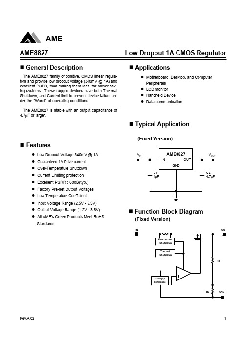
AME8827
Low Dropout 1A CMOS Regulator
n Pin Configuration
SOT-223 Top View
AME8827
AME8827-AGTxxx 1. IN 2. GND (TAB) 3. OUT
MEMORY存储芯片MAX487EEPA+中文规格书

General DescriptionThe MAX481E, MAX483E, MAX485E, MAX487E–MAX491E, and MAX1487E are low-power transceivers forRS-485 and RS-422 communications in harsh environ-ments. Each driver output and receiver input is protectedagainst ±15kV electro-static discharge (ESD) shocks,without latchup. These parts contain one driver and onereceiver. The MAX483E, MAX487E, MAX488E, andMAX489E feature reduced slew-rate drivers that minimizeEMI and reduce reflections caused by improperly termi-nated cables, thus allowing error-free data transmissionup to 250kbps. The driver slew rates of the MAX481E,MAX485E, MAX490E, MAX491E, and MAX1487E are notlimited, allowing them to transmit up to 2.5Mbps.These transceivers draw as little as 120µA supply cur-rent when unloaded or when fully loaded with disableddrivers (see Selector Guide ). Additionally, the MAX481E,MAX483E, and MAX487E have a low-current shutdownmode in which they consume only 0.5µA. All parts oper-ate from a single +5V supply.Drivers are short-circuit current limited, and are protectedagainst excessive power dissipation by thermal shutdowncircuitry that places their outputs into a high-impedancestate. The receiver input has a fail-safe feature that guar-antees a logic-high output if the input is open circuit.The MAX487E and MAX1487E feature quarter-unit-loadreceiver input impedance, allowing up to 128 trans-ceivers on the bus. The MAX488E–MAX491E aredesigned for full-duplex communications, while theMAX481E, MAX483E, MAX485E, MAX487E, andMAX1487E are designed for half-duplex applications.For applications that are not ESD sensitive see the pin-and function-compatible MAX481, MAX483, MAX485,MAX487–MAX491, and MAX1487.ApplicationsLow-Power RS-485 TransceiversLow-Power RS-422 TransceiversLevel TranslatorsTransceivers for EMI-Sensitive Applications Industrial-Control Local Area Networks Next-Generation Device Features ♦For Fault-Tolerant Applications:MAX3430: ±80V Fault-Protected, Fail-Safe, 1/4-Unit Load, +3.3V, RS-485 Transceiver MAX3080–MAX3089: Fail-Safe, High-Speed (10Mbps), Slew-Rate-Limited, RS-485/RS-422Transceivers ♦For Space-Constrained Applications:MAX3460–MAX3464: +5V, Fail-Safe, 20Mbps,Profibus, RS-485/RS-422 Transceivers MAX3362: +3.3V, High-Speed, RS-485/RS-422Transceiver in a SOT23 Package MAX3280E–MAX3284E: ±15kV ESD-Protected,52Mbps, +3V to +5.5V, SOT23, RS-485/RS-422True Fail-Safe Receivers MAX3030E–MAX3033E: ±15kV ESD-Protected,+3.3V, Quad RS-422 Transmitters ♦For Multiple Transceiver Applications:MAX3293/MAX3294/MAX3295: 20Mbps, +3.3V,SOT23, RS-485/RS-422 Transmitters ♦For Fail-Safe Applications:MAX3440E–MAX3444E: ±15kV ESD-Protected,±60V Fault-Protected, 10Mbps, Fail-Safe RS-485/J1708 Transceivers ♦For Low-Voltage Applications:MAX3483E/MAX3485E/MAX3486E/MAX3488E/MAX3490E/MAX3491E: +3.3V Powered, ±15kV ESD-Protected, 12Mbps, Slew-Rate-Limited,True RS-485/RS-422 Transceivers ±15kV ESD-Protected, Slew-Rate-Limited, Low-Power, RS-485/RS-422 TransceiversOrdering InformationOrdering Information continued at end of data sheet.Selector Guide appears at end of data sheet .19-0410; Rev 4; 10/03MAX481E/MAX483E/MAX485E/MAX487E–MAX491E/MAX1487E±15kV ESD-Protected, Slew-Rate-Limited,Low-Power, RS-485/RS-422 Transceivers SWITCHING CHARACTERISTICS—MAX481E/MAX485E, MAX490E/MAX491E, MAX1487EDC ELECTRICAL CHARACTERISTICS (continued)(V CC = 5V ±5%, T A = T MIN to T MAX , unless otherwise noted.) (Notes 1, 2)MAX481E/MAX483E/MAX485E/MAX487E–MAX491E/MAX1487E。
E4B3中文资料

EdalSERIES E4, E7, E8Silicon Power RectifiersEdal Series E power rectifiers are stud mounted DO-4 packages. The silicon junction is carefully fitted within a glass-to-metal hermetically sealed case, reliable operation is assured, even with extreme humidity and under other severe environmentalconditions. The series E power rectifiers are completely corrosion resistant. A double diffused, passivated junction technique is utilized to provide stable uniform electrical characteristics. Inherent in their design is very low leakage currents and excellent surge handling capability. Standard, bulk avalanche and fast recovery types in voltage ratings from 50 to 1500 volts PIV are available. Series E power rectifiers are also available in reverse polarity offering extended application parameters. Edal Series E power rectifiers are ideal for use in applications where economy, power capability and reliability are demanding considerations.SpecificationsCATHODE TO STUD. FOR ANODE TO STUD ADD SUFFIX “R” TO P/N - EX - E7A3R.TO DESIGNATE FAST RECOVERY TYPES USE LETTERS “R”,“S” OR “T” EX: ES7A3. R=500 nsec, S=200 nsec, T=100 nsec FOR AVALANCHE USE SUFFIX 9 INPLACE OF 3 Ex: E7A9Maximum Operating Frequency 100,000 Cycles per SecondELECTRICAL RATINGSE4 E7E8Maximum Forward Current Single Phase Half Wave Case Temperature O c Io AMPS126 16131 22121 30 Maximum Surge Current Single Cycle Amps200 250 300 Maximum Forward Drop @ 25o C Case Io Amps Vf Volts30 1.3 30 1.2 30 1.2 Maximum Reverse Current FCA @ 150o C ma1.0 1.0 1.0 Maximum I 2T (less than 8ms) Amps 2 – Sec 165 250 350 Reverse Power for Bulk Avalanche (Joules) 0.16 0.16 .16 Storage Temperature o C-55 to +190 -55 to +190 -55 to +190 Operating Temperature o C - 40 to +175-40 to +175- 40 to 175Thermal Impedance Maximum(Junction to Case) o C/Watt Maximum 3.0 2.0 3.0 Jedec StyleDO-4DO-4 DO-4 PIV VOLTS 16 AMP 22 AMP 30 AMPS 50 E4A3 E7A3 E8A3 100 E4B3 E7B3 E8B3 200 E4C3 E7C3 E8C3 250 E4D3 E7D3 E8D3 300 E4E3 E7E3 E8E3 350 E4F3 E7F3 E8F3 400 E4G3 E7G3 E8G3 500 E4H3 E7H3 E8H3 600 E4K3 E7K3 E8K3 700 E4M3 E7M3 E8M3 800 E4N3 E7N3 E8N3 1000 E4P3 E7P3 E8P3 1200 E4R3 E7R3 E8R3 1500E4S3E7S3E8S3元器件交易网元器件交易网。
贴片F系列三极管参数

Base I I N C N N X K N N D N N N N N B N N N N N N N N X N N N N N N N N N N N B P X P ZB X ZB
Package SCD80 URD SOT323 SOT23 SC59 SC59 SOT23 SOT23 SOT23 SOT23 SOT23 SOT23 SOT23 SOT23 SOT23 SOT323 SC59 SC59 SOT23 SC59 SC59 SC59 SC59 SOT23 SC59 SC59 SOT23 SC59 SC59 SC59 SC59 SC59 SOT23 SOT89 SOT89 SOT23 SOT23
Leaded Equivalent/Data uhf varicap 2.5-22pf npn RF fT 8GHz 35V RF pin sw diode npn dtr R1 2k2 40V 100mA npn dtr R1 4k7 40V 100mA fT 12GHz npn RF 4V 12mA 35V RF pin sw diode BF495 RF npn fT 150MHz hfe30-60 dual series HP3820 pin sw diode BF184 BF494 BF184 BF494 BF184 BF494 RF npn fT150MHz hfe60-120 BF495 dual cc HP3820 pin sw diode BF184 BF494 pnp dtr 1k + 1k 50V 500mA pnp dtr 2k2 + 2k2 50V 500mA pnp dtr 4k7+ 4k7 50V 500mA pnp dtr 4k7+ 4k7 50V 500mA pnp dtr 10k + 10k 50V 500mA fT 12GHz npn 6V 20mA npn dtr 1k + 1k 50V 500mA npn dtr 2k2 + 2k2 50V 500mA npn dtr 4k7 + 4k7 50V 500mA npn dtr 4k7 + 4k7 50V 500mA npn dtr 10k + 10k 50V 500mA pnp dtr 2k2 + 10k 50V 100mA pnp dtr 2k2 + 10k 50V 100mA npn dtr 2k2 + 10k 50V 100mA pnp dtr R1 2k2 40V 100mA pnp dtr R1 4k7 40V 100mA pnp dtr R110k 40V 100mA 0.5-3GHz cc pin dual anode npn RF 1.5GHz 300mA BFQ69 npn RF Ft 5.5GHz 100mA microproc -ve reset gen 2.700V BFW92 microproc -ve reset gen 2.800V
4N27.3S中文资料

4N25 4N37
4N26 H11A1
4N27 H11A2
4N28 H11A3
4N35 H11A4
4N36 H11A5
TYPICAL PERFORMANCE CURVES
VF - FORWARD VOLTAGE (V)
Fig. 1 LED Forward Voltage vs. Forward Current (Black Package)
4N26 4N27
0.5
4N28
Collector-Emitter Saturation Voltage
VCE (SAT)
4N35 4N36 4N37
0.3
V
(IC = 0.5 mA, IF = 10 mA)
H11A1 H11A2
H11A3
0.4
H11A4
H11A5
AC Characteristic
Test Conditions
Symbol Device Min
Typ*
Max
Unit
4N25
4N26
4N27
(IF = 10 mA, VCC = 10 V, RL = 100Ω)
4N28 H11A1
2
(Fig.20)
H11A2
Turn-off Time
TOFF
H11A3
µs
H11A4
H11A5
(IC = 2 mA, VCC = 10 V, RL = 100Ω) (Fig.20)
TSTG TOPR TSOL
PD
IF VR IF(pk) PD
VCEO VCBO VECO
PD
-55 to +150 -55 to +100 260 for 10 sec
AMIS42700WCGA4RH资料
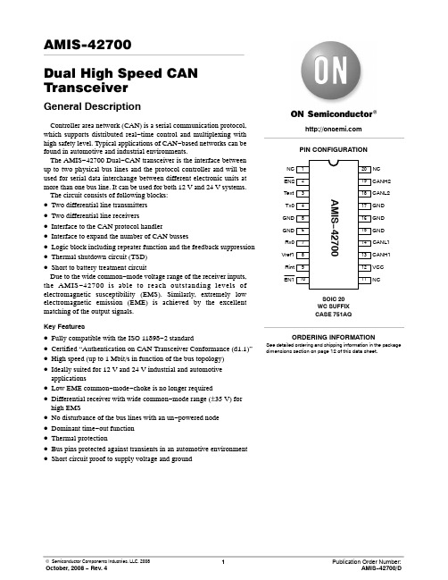
AMIS-42700Dual High Speed CAN TransceiverGeneral DescriptionController area network (CAN) is a serial communication protocol, which supports distributed real−time control and multiplexing with high safety level. Typical applications of CAN−based networks can be found in automotive and industrial environments.The AMIS−42700 Dual−CAN transceiver is the interface between up to two physical bus lines and the protocol controller and will be used for serial data interchange between different electronic units at more than one bus line. It can be used for both 12 V and 24 V systems. The circuit consists of following blocks:•Two differential line transmitters•Two differential line receivers•Interface to the CAN protocol handler•Interface to expand the number of CAN busses•Logic block including repeater function and the feedback suppression •Thermal shutdown circuit (TSD)•Short to battery treatment circuitDue to the wide common−mode voltage range of the receiver inputs, the AMIS−42700 is able to reach outstanding levels ofelectromagnetic susceptibility (EMS). Similarly, extremely low electromagnetic emission (EME) is achieved by the excellent matching of the output signals.Key Features•Fully compatible with the ISO 11898−2 standard •Certified “Authentication on CAN Transceiver Conformance (d1.1)”•High speed (up to 1 Mbit/s in function of the bus topology)•Ideally suited for 12 V and 24 V industrial and automotive applications•Low EME common−mode−choke is no longer required •Differential receiver with wide common−mode range (±35 V) for high EMS•No disturbance of the bus lines with an un−powered node •Dominant time−out function•Thermal protection•Bus pins protected against transients in an automotive environment •Short circuit proof to supply voltage and groundSOIC 20WC SUFFIXCASE 751AQSee detailed ordering and shipping information in the package dimensions section on page 12 of this data sheet.ORDERING INFORMATIONTx0GNDGNDNCRx0Vref1RintEN1NCGNDCANL1CANH1VCCNCGNDGNDCANL2CANH2 TextEN2PIN CONFIGURATIONTable 1. Technical CharacteristicsSymbol Parameter Conditions Min.Max.Unit V CANHx DC voltage at pin CANH1/20 < V CC < 5.25 V; no time limit−45+45V V CANLx DC voltage at pin CANL1/20 < V CC < 5.25 V; no time limit−45+45V V i(dif)(bus_dom)Differential bus output voltage in dominant state42.5 W< R LT < 60 W 1.53V CM−range Input common−mode range for comparator Guaranteed differential receiverthreshold and leakage current−35+35V V CM−peak Common−mode peak See Figures 9 and 10 (Note 1)−10001000mV V CM−step Common−mode step See Figures 9 and 10 (Note 1)−250250mV 1.The parameters V CM−peak and V CM−step guarantee low EME.CANH1CANL1REFCANH2CANL2 Figure 1. Block DiagramTypical ApplicationApplication DescriptionAMIS−42700 is especially designed to provide the link between a CAN controller (protocol IC) and two physical busses. It is able to operate in three different modes:•Dual CAN•A CAN−bus extender •A CAN−bus repeaterApplication SchematicsFigure 2. Application Diagram CAN−bus RepeaterFigure 3. Application Diagram Dual−CANFigure 4. Application Diagram CAN−bus Extender Table 2. Pin OutPin Name Description1NC Not connected2ENB2Enable input, bus system 2; internal pull−up3Text Multi−system transmitter Input; internal pull−up4Tx0Transmitter input; internal pull−up5GND Ground connection (Note 2)6GND Ground connection (Note 2)7Rx0Receiver output8V REF1Reference voltage9Rint Multi−system receiver output10ENB1Enable input, bus system 1; internal pull−up11NC Not connected12VCC Positive supply voltage13CANH1CANH transceiver I/O bus system 114CANL1CANL transceiver I/O bus system 115GND Ground connection (Note 2)16GND Ground connection (Note 2)17GND Ground connection (Note 2)18CANL2CANL transceiver I/O bus system 219CANH2CANH transceiver I/O bus system 220NC Not connected2.In order to ensure the chip performance, all these pins need to be connected to GND on the PCB.Functional DescriptionOverall Functional DescriptionAMIS−42700 is specially designed to provide the link between the protocol IC (CAN controller) and two physical bus lines. Data interchange between those two bus lines is realized via the logic unit inside the chip. To provide an independent switch−off of the transceiver units for both bus systems by a third device (e.g. the m C), enable−inputs for the corresponding driving and receiving sections are provided. As long as both lines are enabled, they appear as one logical bus to all nodes connected to either of them.The bus lines can have two logical states, dominant or recessive. A bus is in the recessive state when the driving sections of all transceivers connected to the bus are passive. The differential voltage between the two wires is approximately zero. If at least one driver is active, the bus changes into the dominant state. This state is represented by a differential voltage greater than a minimum threshold and therefore by a current flow through the terminating resistors of the bus line. The recessive state is overwritten by the dominant state.In case of a fault (like short circuit) is present on one of the bus lines, it remains limited to that bus line where it occurs. Data interchange from the protocol IC to the other bus system and on this bus system itself can be continued. AMIS−42700 can be also used for only one bus system. If the connections for the second bus system are simply left open it serves as a single transceiver for an electronic unit. For correct operation, it is necessary to terminate the open bus by the proper termination resistor.Logic Unit and CAN Controller InterfaceThe logic unit inside AMIS−42700 provides data transfer from/to the digital interface to/from the two busses and from one bus to the other bus. The detailed function of the logic unit is described in Table 3.All digital input pins, including ENBx, have an internal pull-up resistor to ensure a recessive state when the input is not connected or is accidentally interrupted. A dominant state on the bus line is represented by a low-level at the digital interface; a recessive state is represented by a high-level.Dominant state received on any bus (if enabled) causes a dominant state on both busses, pin Rint and pin Rx0. Dominant signal on any of the input pins Tx0 and Text causes transmission of dominant on both bus lines (if enabled).Digital inputs Tx0 and Text are used for connecting the internal logic’s of several IC’s to obtain versions with more than two bus outputs (see Figure 4: Application Diagram CAN-bus Extender). They have also a direct logical link to pins Rx0 and Rint independently on the EN1x pins −dominant on Tx0 is directly transferred to both Rx0 and Rint pins, dominant on Text is only transferred to Rx0. TransmittersThe transceiver includes two transmitters, one for each bus line, and a driver control circuit. Each transmitter is implemented as a push and a pull driver. The drivers will be active if the transmission of a dominant bit is required. During the transmission of a recessive bit all drivers are passive. The transmitters have a built−in current limiting circuit that protects the driver stages from damage caused by accidental short circuit to either positive supply voltage or to ground. Additionally a thermal protection circuit is integrated.The driver control circuit ensures that the drivers are switched on and off with a controlled slope to limit EME. The driver control circuit will be controlled itself by the thermal protection circuit, the timer circuit and the logic unit.The enable signal ENBx allows the transmitter to be switched off by a third device (e.g. the m C). In the disabled state (ENBx = high) the corresponding transmitter behaves as in the recessive state.Table 3. Function of the Logic Unit (bold letters describe input signals)EN1B EN2B TX0TEXT Bus 1 State Bus 2 State RX0RINT 0000dominant dominant00 0001dominant dominant00 0010dominant dominant01 0011recessive recessive11 0011dominant (Note 3)dominant00 0011dominant dominant (Note 3)00 0100dominant recessive00 0101dominant recessive00 0110dominant recessive01 0111recessive recessive11 0111dominant (Note 3)recessive00 3.Dominant detected by the corresponding receiver.Table 3. Function of the Logic Unit (bold letters describe input signals)EN1B RINTRX0Bus 2 StateBus 1 StateTEXTTX0EN2B0111recessive dominant (Note 3)11 1000recessive dominant00 1001recessive dominant00 1010recessive dominant01 1011recessive recessive11 1011dominant (Note 3)recessive11 1011recessive dominant (Note 3)00 1100recessive recessive00 1101recessive recessive00 1110recessive recessive01 1111recessive recessive11 1111dominant (Note 3)recessive11 1111recessive dominant (Note 3)11 3.Dominant detected by the corresponding receiver.ReceiversTwo bus receiving sections sense the states of the bus lines. Each receiver section consists of an input filter and a fast and accurate comparator. The aim of the input filter is to improve the immunity against high−frequency disturbances and also to convert the voltage at the bus lines CANHx and CANLx, which can vary from –12V to +12V, to voltages in the range 0 to 5 V, which can be applied to the comparators.The output signal of the comparators is gated by the ENBx signal. In the disabled state (ENBX = high), the output signal of the comparator will be replaced by a permanently recessive state and does not depend on the bus voltage. In the enabled state the receiver signal sent to the logic unit is identical to the comparator output signal.Time−out CountersTo avoid that the transceiver drives a permanent dominant state on either of the bus lines (blocking all communication), time−out function is implemented. Signals on pins Tx0 and Text as well as both bus receivers are connected to the logic unit through independent timers. If the input of the timer stays dominant for longer than parameter tdom, it’s replaced by a recessive signal on the timer output.Feedback SuppressionThe logic unit described in Table 3 constantly ensures that dominant symbols on one bus line are transmitted to the other bus line without imposing any priority on either of the lines. This feature would lead to an “interlock” state with permanent dominant signal transmitted to both bus lines, if no extra measure is taken.Therefore a feedback suppression is included inside the logic unit of the transceiver. This block masks−out reception on that bus line, on which a dominant is actively transmitted. The reception becomes active again only with certain delay after the dominant transmission on this line is finished. Power−on−Reset (POR)While Vcc voltage is below the POR level, the POR circuit makes sure that:•The counters are kept in the reset mode and stable state without current consumption•Inputs are disabled (don’t care)•Outputs are high impedant; only Rx0 = high−level •Analog blocks are in power down•Oscillator not running and in power down •CANHx and CANLx are recessive•VREF output high impedant for POR not releasedOver Temperature DetectionA thermal protection circuit is integrated to prevent the transceiver from damage if the junction temperature exceeds thermal shutdown level. Because the transmitters dissipate most of the total power, the transmitters will be switched off only to reduce power dissipation and IC temperature. All other IC functions continue to operate. Fault BehaviorA fault like a short circuit is limited to that bus line where it occurs; hence data interchange from the protocol IC to the other bus system is not affected.When the voltage at the bus lines is going out of the normal operating range (−12 V to +12 V), the receiver is not allowed to erroneously detect a dominant state.Short CircuitsAs specified in the maximum ratings, short circuits of the bus wires CANHx and CANLx to the positive supply voltage Vbat or to ground must not destroy the transceiver.A short circuit between CANHx and CANLx must not destroy the IC as well.The dedicated comparator (L2VBAT) on CANL pin detects the short to battery and after debounce time−out switches off the affected driver only. The receiver of the affected driver has to operate normally.Faulty SupplyIn case of a faulty supply (missing connection of the electronic unit or the transceiver to ground, missing connection of the electronic unit to Vbat or missing connection of the transceiver to Vcc), the power supply module of the electronic unit will operate such that the transceiver is not supplied, i.e. the voltage Vcc is below the POR level. In this condition the bus connections of the transceiver must be in the POR state.If the ground line of the electronic unit is interrupted, Vbat may be applied to the Vcc pin (measured relative to the original ground potential, to which the other units on the bus are connected).Reverse Electronic Unit (ECU) SupplyIf the connections for ground and supply voltage of an electronic unit (ECU) (max. 50 V) which provides Vcc for the transceiver are exchanged, this transceiver has a ground potential which may be up to 50 V higher than that of the other transceivers. In this case no transceiver must be destroyed even if several of them are connected via the bus system.Any exchange among the six connections CANH1, CANH2, CANL1, CANL2, ground, and supply voltage of the electronic unit at the connector of the unit must never lead to the destruction of any transceiver of the bus system. Electrical CharacteristicsDefinitionsAll voltages are referenced to GND. Positive currents flow into the IC. Sinking current means that the current is flowing into the pin. Sourcing current means that the current is flowing out of the pin.Absolute Maximum RatingsStresses above those listed in Table 4 may cause permanent device failure. Exposure to absolute maximum ratings for extended periods may affect device reliability.Table 4. Absolute Maximum RatingsSymbol Parameter Conditions Min.Max.Unit V CC Supply voltage−0.3+7V V CANHx DC voltage at pin CANH1/20 < V CC < 5.25 V; no time limit−45+45V V CANLx DC voltage at pin CANL1/20 < V CC < 5.25 V; no time limit−45+45V V digIO DC voltage at digital IO pins (EN1B, EN2B,Rint, Rx0, Text, Tx0)−0.3V CC + 0.3V V REF DC voltage at pin V REF−0.3V CC + 0.3V V tran(CANHx)Transient voltage at pin CANH1/2(Note 4)−150+150V V tran(CANLx)Transient voltage at pin CANL1/2(Note 4)−150+150VV esd(CANLx/CANHx)ESD voltage at CANH1/2 and CANL1/2 pins(Note 5)(Note 7)−4−500+4+500kVVV esd ESD voltage at all other pins(Note 5)(Note 7)−2−250+2+250kVVLatch−up Static latch−up at all pins(Note 6)100mA T stg Storage temperature−55+155°C T amb Ambient temperature−40+125°C T junc Maximum junction temperature−40+150°C4.Applied transient waveforms in accordance with “ISO 7637 part 3”, test pulses 1, 2, 3a, and 3b (see Figure 5).5.Standardized human body model (HBM) ESD pulses in accordance to MIL883 method 3015. Supply pin 8 is ±2 kV.6.Static latch−up immunity: static latch−up protection level when tested according to EIA/JESD78.7.Standardized charged device model ESD pulses when tested according to EOS/ESD DS5.3−1993.Table 5. Thermal CharacteristicsSymbol Parameter Conditions Value Unit R th(vj−a)Thermal resistance from junction to ambient in SO20 package In free air85K/W R th(vj−s)Thermal resistance from junction to substrate of bare die In free air45K/WTable 6. DC and Timing Characteristics (V CC = 4.75 to 5.25 V; T junc = −40 to +150°C; R LT = 60 W unless specified otherwise.) Symbol Parameter Conditions Min.Typ.Max.Unit SUPPLY (pin V CC)I CC Supply current, no loads on digitaloutputs, both busses enabled Dominant transmittedRecessive transmitted45137.519.5mAPORL_VCC Power−on−reset level on V CC 2.2 4.7V DIGITAL INPUTS (Tx0, Text, EN1B, EN2B)V IH High−level input voltage0.7 x V CC−V CC V V IL Low−level input voltage−0.3−0.3 xV CCVI IH High−level input current V IN = V CC−50+5m AI IL Low−level input current V IN = 0 V−75−200−350m AC i Input capacitance Not tested−510pF DIGITAL OUTPUTS (pin Rx0, Rint)I oh High−level output current V o= 0.7 x V CC−5−10−15mAI ol Low−level output current V o= 0.3 x V CC51015mA REFERENCE VOLTAGE OUTPUT (pin V REF1)V REF Reference output voltage−50 m A < I VREF < +50 m A0.45 xV CC 0.50 xV CC0.55 xV CCVV REF_CM Reference output voltage for fullcommon mode range −35 V <V CANHx< +35 V;−35 V <V CANLx< +35 V0.40 xV CC0.50 xV CC0.60 xV CCVBUS LINES (pins CANH1/2 and CANL1/2)V o(reces) (CANHx)Recessive bus voltage at pinCANH1/2V Tx0= V CC; no load 2.0 2.5 3.0VV o(reces) (CANLx)Recessive bus voltage at pinCANL1/2V Tx0= V CC; no load 2.0 2.5 3.0VI o(reces) (CANHx)Recessive output current at pinCANH1/2−35 V < V CANHx< +35 V;0 V < V CC < 5.25 V−2.5−+2.5mAI o(reces) (CANLx)Recessive output current at pinCANL1/2−35 V < V CANLx < +35 V;0 V < V CC < 5.25 V−2.5−+2.5mAV o(dom) (CANHx)Dominant output voltage at pinCANH1/2V Tx0 = 0 V 3.0 3.6 4.25VV o(dom) (CANLx)Dominant output voltage at pinCANL1/2V Tx0 = 0 V0. 5 1.4 1.75VV i(dif)(bus)Differential bus output voltage(V CANHx− V CANLx)V Tx0 = 0 V; dominant;42.5 W < R LT < 60 W1.52.253.0VV TxD = V CC;recessive; no load−1200+50mVI o(sc) (CANHx)Short circuit output current at pinCANH1/2V CANHx = 0 V;V Tx0 = 0 V−45−70−120mAI o(sc)(CANLx)Short circuit output current at pinCANL1/2V CANLx = 36 V;V Tx0 = 0 V (Note 8)4570120mA8.Guaranteed by design for VBAT = 36 V; measured in production for VBAT = 7 V to avoid short−2−VBAT detectionTable 6. DC and Timing Characteristics (V CC = 4.75 to 5.25 V; T junc = −40 to +150°C; R LT = 60 W unless specified otherwise.) Symbol UnitMax.Typ.Min.ConditionsParameterBUS LINES (pins CANH1/2 and CANL1/2)V i(dif)(th)Differential receiver threshold voltage−5 V < V CANLx < +12 V;−5 V < V CANHx < +12 V;see Figure 60.50.70.9VV ihcm(dif)(th)Differential receiver threshold voltagefor high common−mode −35 V < V CANLx < +35 V;−35 V < V CANHx < +35 V;see Figure 60.30.7 1.05VV i(dif)(hys)Differential receiver input voltagehysteresis −35V < V CANL < +35 V;−35 V < V CANH < +35 V;see Figure 65070100mVR i(cm) (CANHx)Common−mode input resistance atpin CANH1/2152637K WR i(cm) (CANLx)Common−mode input resistance atpin CANL1/2152637K WR i(cm)(m)Matching between pin CANH1/2 andpin CANL1/2 common−mode inputresistanceV CANHx = V CANLx−30+3%R i(dif)Differential input resistance255075K W C i(CANHx)Input capacitance at pin CANH1/2V Tx0 = V CC; not tested7.520pF C i(CANLx)Input capacitance at pin CANL1/2V Tx0 = V CC; not tested7.520pFC i(dif)Differential input capacitance V Tx0 = V CC; not tested 3.7510pF I LI(CANHx)Input leakage current at pin CANH1/2V CC < PORL_VCC;−5.25 V < V CANHx < 5.25 V−350170350m AI LI(CANLx)Input leakage current at pin CANL1/2V CC < PORL_VCC;−5.25 V < V CANLx < 5.25 V−350170350m AV CM−peak Common−mode peak during transitionfrom dom → rec or rec → domsee Figure 10−10001000mVV CM−step Difference in common−mode betweendominant and recessive statesee Figure 10−250250mVV CANL2VBAT Detection level for CANL1/2 short toVBAT79.5VTHERMAL SHUTDOWNT j(sd)Shutdown junction temperature150°C TIMING CHARACTERISTICS (see Figures 7 and 8)t d(Tx−BUSon)Delay Tx0/Text to bus active4085120ns t d(Tx−BUSoff)Delay Tx0/Text to bus inactive3060115ns t d(BUSon−RX)Delay bus active to Rx0/Rint2555115ns t d(BUSoff−RX)Delay bus inactive to Rx0/Rint65100145ns t d(ENxB)Delay from EN1B to busactive/inactive100200nst d(Tx−Rx)Delay from Tx0 to Rx0/Rint and fromText to Rx0 (direct logical path)15 pF on the digital output41035nst d(CAN2VBAT)Reaction time of the CANL−to−VBATshort detectorShort occurring14m s Short disappearing1 5.5m st dom Time out counter interval250450750m st d(FBS)Delay for feedbacksuppression release5+t d(BUSon−RX)330ns8.Guaranteed by design for VBAT = 36 V; measured in production for VBAT = 7 V to avoid short−2−VBAT detectionMeasurement Set −ups and DefinitionsSchematics are given for single CAN transceiver.+5VV RxDi(dif)(hys)High LowFigure 5. Test Circuit for Automotive TransientsFigure 6. Hysteresis of the Receiver+5VC LT 100 pFLT 100 pFTx0/Text Rx0/RintV i(dif) =V CANH −t d(Tx −t HIGH LOWFigure 7. Test Circuit for Timing CharacteristicsFigure 8. Timing Diagram for AC CharacteristicsFigure 9. Basic Test Set −up for Electromagnetic MeasurementV i(com)=0.5*(V CANHx +V Figure 10. Common −mode Voltage Peaks (see measurement set −up Figure 9)ORDERING INFORMATIONPart NumberPackageContainerTemperature Range Shipping ConfigurationQuantity AMIS42700WCGA4H SOIC 150 20 300 GREEN Rail 38−40°C to 125°C AMIS42700WCGA4RHSOIC 150 20 300 GREENTape & Reel1500−40°C to 125°CSolderingIntroduction to Soldering Surface Mount Packages This text gives a very brief insight to a complex technology. A more in−depth account of soldering ICs can be found in the ON Semiconductor “Data Handbook IC26; Integrated Circuit Packages” (document order number 9398 652 90011). There is no soldering method that is ideal for all surface mount IC packages. Wave soldering is not always suitable for surface mount ICs, or for printed−circuit boards with high population densities. In these situations reflow soldering is often used.Re−flow SolderingRe−flow soldering requires solder paste (a suspension of fine solder particles, flux and binding agent) to be applied to the printed−circuit board by screen printing, stenciling or pressure−syringe dispensing before package placement. Several methods exist for re−flowing; for example, infrared/convection heating in a conveyor type oven. Throughput times (preheating, soldering and cooling) vary between 100 and 200 seconds depending on heating method. Typical re−flow peak temperatures range from 215°C to 260°C.Wave SolderingConventional single wave soldering is not recommended for surface mount devices (SMDs) or printed−circuit boards with a high component density, as solder bridging and non−wetting can present major problems. To overcome these problems the double−wave soldering method was specifically developed.If wave soldering is used the following conditions must be observed for optimal results:•Use a double−wave soldering method comprising a turbulent wave with high upward pressure followed by a smooth laminar wave.•For packages with leads on two sides and a pitch (e):•Larger than or equal to 1.27 mm, the footprint longitudinal axis is preferred to be parallel to thetransport direction of the print−circuit board;•Smaller than 1.27 mm, the footprintlongitudinal axis must be parallel to thetransport direction of the printed−circuit board.The footprint must incorporate solder thieves atthe downstream end.•For packages with leads on four sides, the footprint must be placed at a 45° angle to the transport direction of the printed−circuit board. The footprint must incorporate solder thieves downstream and at the side corners. During placement and before soldering, the package must be fixed with a droplet of adhesive. The adhesive can be applied by screen printing, pin transfer or syringe dispensing. The package can be soldered after the adhesive is cured. Typical dwell time is four seconds at 250°C. A mildly−activated flux will eliminate the need for removal of corrosive residues in most applications.Manual SolderingFix the component by first soldering two diagonally−opposite end leads. Use a low voltage (24 V or less) soldering iron applied to the flat part of the lead. Contact time must be limited to 10 seconds at up to 300°C. When using a dedicated tool, all other leads can be soldered in one operation within two to five seconds between 270°C and 320°C.Table 7. Soldering ProcessPackageSoldering MethodWave Re−flow (Note 9)BGA, SQFP Not suitable SuitableHLQFP, HSQFP, HSOP, HTSSOP, SMS Not suitable (Note 10)SuitablePLCC (Note 11), SO, SOJ Suitable SuitableLQFP, QFP, TQFP Not recommended (Notes 11 and 12)SuitableSSOP, TSSOP, VSO Not recommended (Note 13)Suitable9.All SMD packages are moisture sensitive. Depending upon the moisture content, the maximum temperature (with respect to time) and bodysize of the package, there is a risk that internal or external package cracks may occur due to vaporization of the moisture in them (the so called popcorn effect). For details, refer to the dry pack information in the “Data Handbook IC26; Integrated Circuit Packages; Section: Packing Methods”.10.These packages are not suitable for wave soldering as a solder joint between the printed−circuit board and heatsink (at bottom version) cannot be achieved, and as solder may stick to the heatsink (on top version).11.If wave soldering is considered, then the package must be placed at a 45° angle to the solder wave direction. The package footprint mustincorporate solder thieves downstream and at the side corners.12.Wave soldering is only suitable for LQFP, TQFP and QFP packages with a pitch (e) equal to or larger than 0.8 mm; it is definitely not suitablefor packages with a pitch (e) equal or smaller than 0.65 mm.13.Wave soldering is only suitable for SSOP and TSSOP packages with a pitch (e) equal to or larger than 0.65 mm; it is definitely not suitablefor packages with a pitch (e) equal to or smaller than 0.5 mm.PACKAGE DIMENSIONSSOIC 20 W CASE 751AQ −01ISSUE OON Semiconductor and are registered trademarks of Semiconductor Components Industries, LLC (SCILLC). SCILLC reserves the right to make changes without further notice to any products herein. SCILLC makes no warranty, representation or guarantee regarding the suitability of its products for any particular purpose, nor does SCILLC assume any liability arising out of the application or use of any product or circuit, and specifically disclaims any and all liability, including without limitation special, consequential or incidental damages.“Typical” parameters which may be provided in SCILLC data sheets and/or specifications can and do vary in different applications and actual performance may vary over time. All operating parameters, including “Typicals” must be validated for each customer application by customer’s technical experts. SCILLC does not convey any license under its patent rights nor the rights of others. SCILLC products are not designed, intended, or authorized for use as components in systems intended for surgical implant into the body, or other applications intended to support or sustain life, or for any other application in which the failure of the SCILLC product could create a situation where personal injury or death may occur. Should Buyer purchase or use SCILLC products for any such unintended or unauthorized application, Buyer shall indemnify and hold SCILLC and its officers, employees, subsidiaries, affiliates,and distributors harmless against all claims, costs, damages, and expenses, and reasonable attorney fees arising out of, directly or indirectly, any claim of personal injury or death associated with such unintended or unauthorized use, even if such claim alleges that SCILLC was negligent regarding the design or manufacture of the part. SCILLC is an Equal Opportunity/Affirmative Action Employer. This literature is subject to all applicable copyright laws and is not for resale in any manner.PUBLICATION ORDERING INFORMATION。
NCV4275中文资料

NCV4275中⽂资料NCV42755.0 V Low?Drop Voltage RegulatorThis industry standard linear regulator has the capability to drive loads up to 450 mA at 5.0 V. It is available in DPAK and D2PAK. This device is pin?for?pin compatible with Infineon part number TLE4275.Features5.0 V, ±2%, 450 mA Output VoltageV ery Low Current ConsumptionActive RESETReset Low Down to V Q = 1.0 V500 mV (max) Dropout V oltageFault Protection+45 V Peak Transient V oltage42 V Reverse V oltageShort CircuitThermal OverloadNCV Prefix for Automotive and Other Applications Requiring Site and Control ChangesIDQGNDROFigure 1. Block Diagram/doc/4600ca242af90242a895e51d.htmlD2PAK5?PINDS SUFFIXCASE 936ADPAK5?PINDT SUFFIXCASE 175AAPin 1. I2. ROTab,3. GND*4. D5. Q* T ab is connected toPin 3 on all packagesDevice Package Shipping?ORDERING INFORMATIONNCV4275DT DPAK75 Units/Rail NCV4275DTRK DPAK2500 T ape & Reel NCV4275DS D2PAK50 Units/RailNCV4275DSR4D2PAK800 T ape & Reel ?For information on tape and reel specifications, including part orientation and tape sizes, please refer to our T ape and Reel Packaging Specification Brochure, BRD8011/D.MARKINGDIAGRAMSNCV4275AWLYYWW11A= Assembly LocationWL, L= Wafer LotYY, Y= YearWW= Work WeekPIN FUNCTION DESCRIPTIONMAXIMUM RATINGS?(not normal operating conditions) and are not valid simultaneously. If these limits are exceeded, device functional operation is not implied, damage may occur and reliability may be affected.THERMAL CHARACTERISTICS2.10 seconds max.3.?5°C/+0°C allowable conditions.4. 1 oz. copper, 0.26 inch2 (168 mm2) copper area, 0.62″thick FR4.5. 1 oz. copper, 1.14 inch2 (736 mm2) copper area, 0.62″thick FR4.6. 1 oz. copper, 0.373 inch2 (241 mm2) copper area, 0.62″thick FR4.7. 1 oz. copper, 1.222 inch2 (788 mm2) copper area, 0.62″thick FR4.During the voltage range which exceeds the maximum tested voltage of I, operation is assured, but not specified. Wider limits may apply. Thermal dissipation must be observed closely.ELECTRICAL CHARACTERISTICS (I = 13.5 V; ?40°C < T< 150°C; unless otherwise noted)OutputReset Timing D and Output RO TYPICAL PERFORMANCE CHARACTERISTICSFigure 2. Output Stability with OutputCapacitor ESROUTPUT CURRENT (mA)E S R (W )100200300400500APPLICATION INFORMATIONV IV QV RO Figure 3. Test CircuitCircuit DescriptionThe error amplifier compares a temperature?stable reference voltage to a voltage that is proportional to the output voltage (Q) (generated from a resistor divider) and drives the base of a series transistor via a buffer. Saturation control as a function of the load current prevents oversaturation of the output power device, thus preventing excessive substrate current (quiescent current).Typical drop out voltage at 300 mA load is 250 mV, 500 mV maximum. Test voltage for drop out is 5.0 V input. Stability ConsiderationsThe input capacitors (C I1 and C I2) are necessary to control line influences. Using a resistor of approximately 1.0 ? in series with C I2 can solve potential oscillations due to stray inductance and capacitance.The output or compensation capacitor helps determine three main characteristics of a linear regulator: start?up delay, loadtransient response and loop stability.The capacitor value and type should be based on cost, availability, size and temperature constraints. A tantalum or aluminum electrolytic capacitor is best, since a film or ceramic capacitor with almost zero ESR can cause instability. The aluminum electrolytic capacitor is the least expensive solution, but, if the circuit operates at low temperatures (?25°C to ?40°C), both the value and ESR of the capacitor will vary considerably. The capacitor manufacturers data sheet usually provides this information.The value for the output capacitor C Q shown in Figure 3 should work for most applications, however it is not necessarily the optimized solution. Stability is guaranteed for C Q > 22 m F and an ESR ≤ 5.0 ?.Calculating Power Dissipationin a Single Output Linear RegulatorThe maximum power dissipation for a single output regulator (Figure 4) is:P D(max)+[V I(max)*V Q(min)]I Q(max)(1) )V I(max)I qwhereV I(max)is the maximum input voltage,V Q(min)is the minimum output voltage,I Q(max)is the maximum output current for theapplication,I q is the quiescent current the regulatorconsumes at I Q(max).Once the value of P D(max) is known, the maximum permissible value of R q JA can be calculated:R q JA+150°C*T AD(2) The value of R q JA can then be compared with those in the package section of the data sheet. Those packages with R q JA’s less than the calculated value in Equation 2 will keep the die temperature below 150°C.In some cases, none of the packages will be sufficient to dissipate the heat generated by the IC, and an external heatsink will be required.Figure 4. Single Output Regulator with KeyPerformance Parameters LabeledV I V QHeat SinksA heat sink effectively increases the surface area of the package to improve the flow of heat away from the IC and into the surrounding air.Each material in the heat flow path between the IC and the outside environment will have a thermal resistance.Like series electrical resistances, these resistances are summed to determine the value of R q JA :R q JA +R q JC )R q CS )R q SA(3)whereR q JC is the junction?to?case thermal resistance,R q CS is the case?to?heatsink thermal resistance,R q SA is the heatsink?to?ambient thermalresistance.R q JC appears in the package section of the data sheet.Like R q JA , it too is a function of package type. R q CSand R q SA are functions of the package type, heatsink and the interface between them. These values appear in heat sink data sheets of heat sink manufacturers.Thermal, mounting, and heatsinking considerations are discussed in the ON Semiconductor application noteAN1040/D.VV Delay TimeReaction TimePower?on?ResetThermal ShutdownVoltage Dip at InputUndervoltageSecondary SpikeOverload at OutputFigure 5. Reset TimingThe Cauer networks generally have physical significance and may be divided between nodes to separate thermal behavior due to one portion of the network from another. The Foster networks, though when sorted by time constant (as above) bear a rough correlation with the Cauer networks, are really only convenient mathematical models. Cauer networks can be easily implemented using circuit simulating tools, whereas Foster networks may be more easily implemented using mathematical tools (for instance, in a spreadsheet program), according to the following formula:R(t)+n Si+1R iǒ1?e?tńtau iǔ150Figure 6. q JA vs. Copper Spreader Area,DPAK 5?Lead Figure 7. q JA vs. Copper Spreader Area,D 2PAK 5?Lead200250300350400450500550600650700750COPPER AREA (mm 2)q J A(C °/W )150200250300350400450500550600650700750 COPPER AREA (mm 2)100101.00.10.01TIME (sec)R (t ) C °/W0.00000010.0000010.000010.00010.0010.010.1 1.010******* Figure 8. Single?Pulse Heating Curves, DPAK 5?Lead 100101.00.10.01TIME (sec)R (t ) C °/W0.00000010.0000010.000010.00010.0010.010.1 1.010******* Figure 9. Single?Pulse Heating Curves, D 2PAK 5?Lead 100101.00.10.01PULSE WIDTH (sec)R q J A 788 m m 2 C °/W0.00000010.0000010.000010.00010.0010.010.11.0101001000100101.00.10.01PULSE WIDTH (sec)R q J A 736 m m 2 C °/W0.00000010.0000010.000010.00010.0010.010.11.0101001000Figure 10. Duty Cycle for 1” Spreader Boards, DPAK 5?LeadFigure 11. Duty Cycle for 1” Spreader Boards, D 2PAK 5?LeadR R RR Figure 12. Grounded Capacitor Thermal Network (“Cauer” Ladder) R R R R time constant; amplitudes are the resistances.(thermal ground) Figure 13. Non?Grounded Capacitor Thermal Ladder (“Foster” Ladder) DPAK 5 CENTER LEAD CROPDT SUFFIXCASE 175AA?01ISSUE ONOTES:D 2PAK 5 LEAD DS SUFFIX CASE 936A?02ISSUE B5 REFNOTES:1.DIMENSIONING AND TOLERANCING PER ANSI Y14.5M, 1982.2.CONTROLLING DIMENSION: INCH.3.TAB CONTOUR OPTIONAL WITHIN DIMENSIONS A AND K.4.DIMENSIONS U AND V ESTABLISH A MINIMUM MOUNTING SURFACE FOR TERMINAL 6.5.DIMENSIONS A AND B DO NOT INCLUDE MOLD FLASH OR GATE PROTRUSIONS. MOLD FLASH AND GATE PROTRUSIONS NOT TO EXCEED 0.025 (0.635) MAXIMUM.DIM A MIN MAX MIN MAX MILLIMETERS 0.3860.4039.80410.236INCHES B 0.3560.3689.0429.347C 0.1700.180 4.318 4.572D 0.0260.0360.6600.914E 0.0450.055 1.143 1.397G 0.067 BSC 1.702 BSC H 0.5390.57913.69114.707K 0.050 REF 1.270 REF L 0.0000.0100.0000.254M 0.0880.102 2.235 2.591N 0.0180.0260.4570.660P 0.0580.078 1.473 1.981R 5 REF S 0.116 REF 2.946 REF U 0.200 MIN 5.080 MIN V0.250 MIN6.350 MIN__ON Semiconductor and are registered trademarks of Semiconductor Components Industries, LLC (SCILLC). SCILLC reserves the right to make changes without further notice to any products herein. SCILLC makes no warranty, representation or guarantee regarding the suitability of its products for any particular purpose, nor does SCILLC assume any liability arising out of the application or use of any product or circuit, and specifically disclaims any and all liability, including without limitation special, consequential or incidental damages. “Typical” parameters which may be provided in SCILLC data sheets and/or specifications can and do vary in different applications and actual performance may vary over time. All operating parameters, including “Typicals” must be validated for each customer application by customer’s technical experts. SCILLC does not convey any license under its patent rights nor the rights of others. SCILLC products are not designed, intended, or authorized for use as components in systems intended for surgical implant into the body, or other applications intended to support or sustain life, or for any other application in which the failure of the SCILLC product could create a situation where personal injury or death may occur. Should Buyer purchase or use SCILLC products for any such unintended or unauthorized application, Buyer shall indemnify and hold SCILLC and its officers, employees, subsidiaries, affiliates, and distributors harmless against all claims, costs, damages, and expenses, and reasonable attorney fees arising out of, directly or indirectly, any claim of personal injury or death associated with such unintended or unauthorized use, even if such claim alleges that SCILLC was negligent regarding the design or manufacture of the part.SCILLC is an Equal Opportunity/Affirmative Action Employer. This literature is subject to all applicable copyright laws and is not for resale in any manner. PUBLICATION ORDERING INFORMATION。
A6273中文资料

Data Sheet26180.1208-BIT LATCHEDDMOS POWER DRIVERThe A6273KA and A6273KLW combine eight (positive-edge-triggered D-type) data latches and DMOS outputs for systems requiring relatively high load power. Driver applications include relays, sole-noids, and other medium-current or high-voltage peripheral power loads.The CMOS inputs and latches allow direct interfacing with microproces-sor-based systems. Use with TTL may require appropriate pull-up resistors to ensure an input logic high.The DMOS output inverts the DATA input. All of the output drivers are disabled (the DMOS sink drivers turned OFF) with theCLEAR input low. The A6273KA/KLW DMOS open-drain outputs are capable of sinking up to 750 mA. Similar devices with reduced r DS(on)will be available as the A6A273.The A6273KA is furnished in a 20-pin dual in-line plastic package.The A6273KLW is furnished in a 20-lead wide-body, small-outline plastic package (SOIC) with gull-wing leads for surface-mount applica-tions. Copper lead frames, reduced supply current requirements, and low on-state resistance allow both devices to sink 150 mA from all outputs continuously, to ambient temperatures over 85°C.FEATURESI 50 V Minimum Output Clamp VoltageI 250 mA Output Current (all outputs simultaneously)I 1.3 Ω Typical r DS(on)I Low Power ConsumptionI Replacements for TPIC6273N and TPIC6273DW6273ADVANCE INFORMATION(Subject to change without notice)January 24, 2000Always order by complete part number:Part Number Package R θJAR θJC A6273KA 20-pin DIP 55°C/W 25°C/W A6273KLW 20-lead SOIC70°C/W 17°C/W62738-BIT LATCHEDDMOS POWER DRIVER115 Northeast Cutoff, Box 15036Worcester, Massachusetts 01615-0036 (508) 853-5000Copyright © 2000, Allegro MicroSystems, Inc.LOGIC SYMBOL4567141516171211Dwg. FP-046-13891213181950751001251502.50.5A L L O W AB L E P AC K A G E P O W E RD I S S I P A T I O N I N W A T T SAMBIENT TEMPERATURE IN °C2.01.51.025Dwg. GS-004AS U F FI X'L W ', R =70°C /WθJ A S U F F I X 'A ', R = 55°C /W θJ A FUNCTION TABLEInputs CLEARSTROBEIN XOUT XL XX H H H L H L HHLXRL = Low Logic Level H = High Logic Level X = IrrelevantR = Previous StateDMOS POWER DRIVER OUTPUTLOGIC INPUTSINOUT62738-BIT LATCHEDDMOS POWER DRIVERFUNCTIONAL BLOCK DIAGRAMGROUNDDwg. FP-016-2CLEAR(ACTIVE LOW)LOGIC SUPPLYOUT 1OUT 2OUT 3OUT 4OUT 5OUT 6OUT 7OUT 8IN 2IN IN IN 5IN 6IN IN 8IN STROBE62738-BIT LATCHEDDMOS POWER DRIVER115 Northeast Cutoff, Box 15036Worcester, Massachusetts 01615-0036 (508) 853-5000LimitsCharacteristic Symbol Test Conditions Min.Typ.Max.Units Logic Supply Voltage V DD Operating 4.5 5.0 5.5V Output Breakdown V (BR)DSX I O = 1 mA 50——V Voltage Off-State Output I DSXV O = 40 V—0.05 1.0µA CurrentV O = 40 V T A = 125°C—0.15 5.0µA Static Drain-Source r DS(on)I O = 250 mA, V DD = 4.5 V— 1.3 2.0ΩOn-State ResistanceI O = 250 mA, V DD = 4.5 V, T A = 125°C — 2.0 3.2ΩI O = 500 mA, V DD = 4.5 V (see note)— 1.3 2.0ΩNominal Output I O(nom)V DS(on) = 0.5 V, T A = 85°C —250—mA CurrentLogic Input CurrentI IH V I = V DD = 5.5 V —— 1.0µA I ILV I = 0, V DD = 5.5 V ——-1.0µA Prop. Delay Timet PLH I O = 250 mA, C L = 30 pF —625—ns t PHLI O = 250 mA, C L = 30 pF —150—ns Output Rise Time t r I O = 250 mA, C L = 30 pF —675—ns Output Fall Time t f I O = 250 mA, C L = 30 pF —400—ns Supply CurrentI DD(off)V DD = 5.5 V, Outputs OFF —15100µA I DD(on)V DD = 5.5 V, Outputs ON—150300µATypical Data is at V DD = 5 V and is for design information only.NOTE — Pulse test, duration ≤100 µs, duty cycle ≤2%.ELECTRICAL CHARACTERISTICS at T A = +25°C, V DD = 5 V, t ir = t if ≤ 10 ns (unless otherwise specified).RECOMMENDED OPERATING CONDITIONSover operating temperature rangeLogic Supply Voltage Range, V DD ............... 4.5 V to 5.5 V High-Level Input Voltage, V IH ............................ ≥ 0.85V DD Low-level input voltage, V IL ................................. ≤0.15V DD62738-BIT LATCHEDDMOS POWER DRIVERTIMING REQUIREMENTSOUTPUTxDwg. WP-036-1INxSTROBEInput Active Time Before Strobe(Data Set-Up Time), t su(D).............................................. 20 ns Input Active Time After Strobe(Data Hold Time), t h(D)................................................... 20 ns Input Pulse Width, t w(D)...................................................... 40 ns Input Logic High, V IH ................................................ ≥ 0.85V DD Input Logic Low, V IL ................................................. ≤ 0.15V DD62738-BIT LATCHEDDMOS POWER DRIVER115 Northeast Cutoff, Box 15036Worcester, Massachusetts 01615-0036 (508) 853-5000TEST CIRCUITSI V = 1.0 ASingle-Pulse Avalanche Energy Test Circuitand WaveformsE AS = I AS x V (BR)DSX x t AV /262738-BIT LATCHED DMOS POWER DRIVER TERMINAL DESCRIPTIONSTerminal No.Terminal Name Function1CLEAR When (active) LOW, all latches are reset and all outputs go HIGH (turn OFF).2IN1CMOS data input to a latch. When strobed, the output then inverts the datainput (IN1 = HIGH, OUT1 = LOW).3IN2CMOS data input to a latch. When strobed, the output then inverts the datainput (IN2 = HIGH, OUT2 = LOW).4OUT1Current-sinking, open-drain DMOS output.5OUT2Current-sinking, open-drain DMOS output.6OUT3Current-sinking, open-drain DMOS output.7OUT4Current-sinking, open-drain DMOS output.8IN3CMOS data input to a latch. When strobed, the output then inverts the datainput (IN3 = HIGH, OUT3 = LOW).9IN4CMOS data input to a latch. When strobed, the output then inverts the datainput (IN4 = HIGH, OUT4 = LOW).10GROUND Reference terminal for all voltage measurements.11STROBE A CMOS dynamic input to all latches. Data on each IN x terminal is loadedinto its associated latch on a low-to-high STROBE transition.12IN5CMOS data input to a latch. When strobed, the output then inverts the datainput (IN5 = HIGH, OUT5 = LOW).13IN6CMOS data input to a latch. When strobed, the output then inverts the datainput (IN6 = HIGH, OUT6 = LOW).14OUT5Current-sinking, open-drain DMOS output.15OUT6Current-sinking, open-drain DMOS output.16OUT7Current-sinking, open-drain DMOS output.17OUT8Current-sinking, open-drain DMOS output.18IN7CMOS data input to a latch. When strobed, the output then inverts the datainput (IN7 = HIGH, OUT7 = LOW).19IN8CMOS data input to a latch. When strobed, the output then inverts the datainput (IN8 = HIGH, OUT8 = LOW).20LOGIC SUPPLY(V DD) The logic supply voltage (typically 5 V).62738-BIT LATCHEDDMOS POWER DRIVER115 Northeast Cutoff, Box 15036Worcester, Massachusetts 01615-0036 (508) 853-5000A6273KADimensions in Inches (controlling dimensions)Dimensions in Millimeters (for reference only)NOTES:1.Exact body and lead configuration at vendor’s option within limits shown.2.Lead spacing tolerance is non-cumulative.3.Lead thickness is measured at seating plane or below.Dwg. MA-001-20 mm110Dwg. MA-001-20 in11062738-BIT LATCHED DMOS POWER DRIVERA6273KLWDimensions in Inches(for reference only)Dimensions in Millimeters (controlling dimensions)Dwg. MA-008-20 mm1.27BSCNOTES:1.Exact body and lead configuration at vendor’s option within limits shown.2.Lead spacing tolerance is non-cumulative.62738-BIT LATCHEDDMOS POWER DRIVER115 Northeast Cutoff, Box 15036Worcester, Massachusetts 01615-0036 (508) 853-5000The products described here are manufactured under one or more U.S. patents or U.S. patents pending.Allegro MicroSystems, Inc. reserves the right to make, from time to time, such departures from the detail specifications as may berequired to permit improvements in the performance, reliability, or manufacturability of its products. Before placing an order, the user is cautioned to verify that the information being relied upon is current.Allegro products are not authorized for use as critical components in life-support devices or systems without express written approval.The information included herein is believed to be accurate and reliable. However, Allegro MicroSystems, Inc. assumes no responsi-bility for its use; nor for any infringement of patents or other rights of third parties which may result from its use.。
- 1、下载文档前请自行甄别文档内容的完整性,平台不提供额外的编辑、内容补充、找答案等附加服务。
- 2、"仅部分预览"的文档,不可在线预览部分如存在完整性等问题,可反馈申请退款(可完整预览的文档不适用该条件!)。
- 3、如文档侵犯您的权益,请联系客服反馈,我们会尽快为您处理(人工客服工作时间:9:00-18:30)。
in SIEGET 25-TechnologieSi-MMIC-Amplifier • Cascadable 50 Ω-gain block • Unconditionally stable• Gain |S 21|2 = 18.5 dB at 1.8 GHz (Appl.1) gain |S 21|2 = 22 dB at 1.8 GHz (Appl.2) I P 3out = +7 dBm at 1.8 GHz (V D =3V, I D =9.4mA)• Noise figure NF = 2.2 dB at 1.8 GHz • Typical device voltage V D = 2 V to 5 V • Reverse isolation > 35 dB (Appl.2)• Pb-free (RoHS compliant) package 1)VCircuit DiagramESD (E lectro s tatic d ischarge) sensitive device, observe handling precaution!Type Marking Pin Configuration Package BGA427BMs1, IN2, GND 3, +V4, OutSOT343Maximum Ratings Parameter Symbol Value Unit Device current I D 25mA Device voltageV D ,+V 6V Total power dissipation T S = 120 °C P tot 150mW RF input power P RFin -10dBm Junction temperature T j 150°CAmbient temperature range T A -65 ... 150Storage temperature range T stg-65 (150)Thermal Resistance Junction - soldering point 2)R thJS ≤ 295K/W1Pb-containing package may be available upon special request2For calculation of RthJA please refer to Application Note Thermal ResistanceElectrical Characteristics at T A = 25 °C, unless otherwise specified.Parameter Symbol ValuesUnitmin.typ.max.AC characteristics V D = 3 V, Z o = 50Ω, Testfixture Appl.1Insertion power gain f = 0.1 GHz f = 1 GHz f = 1.8 GHz |S 21|2--- 272218.5 ---dBReverse isolation f = 1.8 GHz S12-22-Noise figure f = 0.1 GHz f = 1 GHz f = 1.8 GHzNF--- 1.922.2 ---Intercept point at the output f = 1.8 GHzIP 3out -+ 7 -dBm Return loss input f = 1.8 GHzRL in ->12-dBReturn loss output f = 1.8 GHzRL out->9-Typical configuration Appl.1Appl.2100 pFEHA07379100 pF100 pF1 nFRF OUTRF INGND+VBGA 427Note: 1) Large-value capacitors should be connected from pin 3 to ground right at the device to provide a low impedance path (appl.1).2) The use of plated through holes right at pin 2 is essential for pc-board-applications. Thin boards are recommended to minimize the parasitic inductance to ground.S-Parameters at T A = 25 °C, (Testfixture, Appl.1)f S 11S 21S 12S 22GHzMAGANGMAGANGMAGANGMAGANGV D = 3V, Z o = 50Ω0.10.20.50.80.911.51.81.922.530.13820.11790.16970.18240.17820.1760.18270.19690.20210.21160.24370.258-38.3-16-20.8-56.9-69.1-80.6-133.5-156.1-162.8-167.7172.8153.324.82124.60622.23618.25817.15215.78610.9239.0298.4868.0156.2595.103164.9158.9135.2115.4109.410484.97774.772.363550.00220.00460.01040.01690.01940.02250.03850.04790.05170.05490.07090.089250.771.883.894.897.398.399.799.398.998.897.196.90.64350.62780.540.44530.43260.41290.38520.39170.39460.39910.42020.4477174.8166.9147.3140.2139.4138.1139.6139.3138.8138.3134.6131Spice-model BGA 427T1T501T2T501R 114.5k ΩR 2280ΩR 3 2.4k ΩR 4170ΩC 1 2.3pF C P10.2pF 0.2pF C P2C P30.6pFC P40.1pF C P50.1pF C'-E'-diode T1Transistor Chip Data T1 (Berkley-SPICE 2G.6 Syntax) :IS =0.21024fA V 39.251VAF =NE = 1.7763-V VAR =34.368NC = 1.3152-ΩRBM = 1.3491CJE = 3.7265fF ps 4.5899TF =ITF = 1.3364mA V 0.99532VJC =TR = 1.4935ns -MJS =0XTI =3-BF =83.23-A 0.16493IKF =BR =10.526-A IKR =0.25052RB =15Ω RE = 1.9289VJE =0.70367V -XTF =0.3641PTF =0deg -0.48652MJC =CJS =0fF -XTB =0FC =0.99469-NF = 1.0405-ISE =fA 15.7610.96647-NR =ISC =0.037223fA 0.21215A IRB =RC =Ω0.126910.37747-MJE =VTF =V 0.1976296.941fF CJC =XCJC =0.08161-0.75VVJS =EG = 1.11eV 300KTNOMC'-E'-Diode Data (Berkley-SPICE 2G.6 Syntax) :RS =20ΩIS =2fA -1.02N =All parameters are ready to use, no scaling is necessaryPackage Equivalent Circuit:Extracted on behalf of Infineon Technologies AG by:Institut für Mobil-und Satellitentechnik (IMST)For examples and ready to use parameters please contact your local Infineon Technologies distributor or sales office to obtain a Infineon Technologies CD-ROM or see Internet:/silicondiscretesInsertion power gain |S 21|2 = f (f )V D , I D = parameter1|S 21|2Noise figure NF = f (f )V D ,ID = parameter1N FIntercept point at the output IP 3out = f (f )V D ,I D = parameter1dBmI P 3o u tPublished byInfineon Technologies AG81726 München, Germany© Infineon Technologies AG 2007.All Rights Reserved.Attention please!The information given in this data sheet shall in no event be regarded as a guarantee of conditions or characteristics (“Beschaffenheitsgarantie”). With respect to any examples or hints given herein, any typical values stated herein and/or any information regarding the application of the device, Infineon Technologies hereby disclaims any and all warranties and liabilities of any kind, including without limitation warranties of non-infringement of intellectual property rights of any third party.InformationFor further information on technology, delivery terms and conditions and prices please contact your nearest Infineon Technologies Office (). WarningsDue to technical requirements components may contain dangerous substances.For information on the types in question please contact your nearestInfineon Technologies Office.Infineon Technologies Components may only be used in life-support devices or systems with the express written approval of Infineon Technologies, if a failure of such components can reasonably be expected to cause the failure of thatlife-support device or system, or to affect the safety or effectiveness of thatdevice or system.Life support devices or systems are intended to be implanted in the human body,or to support and/or maintain and sustain and/or protect human life. If they fail,it is reasonable to assume that the health of the user or other personsmay be endangered.。