RT8015资料
8015电源模块电路工作原理

电源模块是电子设备中常见的一个组成部分,它能够将电源输入转换为设备所需的稳定电压输出。
在各种电子设备中,电源模块都扮演着非常重要的角色。
电源模块的工作原理涉及到电路设计、电磁学、控制系统等多个领域的知识,下面我们就来详细介绍一下8015电源模块的工作原理。
一、8015电源模块的基本构成8015电源模块通常由输入端、输出端、控制电路和功率器件四部分组成。
其中输入端接收外部电源输入,输出端输出稳定的电压给设备使用,控制电路负责监测和调节输出电压,功率器件则负责电源的转换和稳定。
二、8015电源模块的工作原理1. 输入端稳压滤波当外部电源接入8015电源模块时,首先经过输入端的稳压滤波电路,这个电路主要作用是对输入的电压进行稳压和滤波处理,确保输入电压的稳定性和纯净性,以防止外部电压的波动和噪声对后续电路产生干扰。
2. 开关电源变换稳压滤波后的电压信号经过控制电路的调度,进入开关电源变换器。
开关电源变换器是8015电源模块的核心部件,它利用高频开关原理,将输入的直流电压转换成高频脉冲电压,再经过变压器和整流滤波电路得到稳定的直流输出电压。
3. 输出端稳压调节经过开关电源变换后的电压信号还需要经过稳压调节电路的调节,最终得到设备所需的稳定输出电压。
稳压调节电路具有过载保护、短路保护、过压保护等功能,能够确保输出电压的稳定性和安全性。
4. 反馈控制在整个电源模块工作过程中,控制电路不断监测输出电压的变化,并通过负反馈控制的方式调节开关电源的工作状态,从而实现对输出电压的精确调控。
这样可以保证在外部负载发生变化时,输出电压能够迅速恢复稳定。
三、8015电源模块的性能特点8015电源模块具有输出电压稳定、效率高、负载能力强、体积小等特点,具体表现在以下几个方面:1. 输出电压稳定性好:在外部电压波动较大或负载突然变化的情况下,输出电压能够保持稳定;2. 效率高:8015电源模块采用先进的开关电源技术,能够将能量转换得非常高效,减小能源的损耗,提高整个系统的能效;3. 负载能力强:在外部负载变化剧烈的情况下,能够迅速调整输出电压,确保设备正常工作;4. 体积小:8015电源模块采用集成化设计,功率器件和控制电路都集成在一块PCB板上,能够大大减小整个模块的体积。
ZXDU58_W121(V1.0)30A系列组合电源用户手册
3. 《ZXD1500(V4.0)30A 开关整流器用户手册》
该手册介绍 ZXD1500(V4.0)整流器的功能特点、性能参数、工作原理、 外形结构、安装调试、使用操作、日常维护和运输存储。本手册适用于安 装人员和操作维护人员。
请在安装、操作和维护前仔细阅读以上手册,并注意设备上的各种警示牌及警示 语句。所有的随机资料阅读完毕后请妥善保存,以便日后查阅。
南京能瑞低压集中器调试资料8015全载波汇总

南京能瑞8015集中器安装与调试一、安装接线图二、安装注意事项1、接线端子2、5、8、10对应的是A、B、C三项电压和零线,1、3端子是A相电流进出线;4、6端子是B相电流进出线;7、9端子是C相电流进出线;2、如果需要终端实现交采计量功能,电压电流需要都接上,不需要则只接A、B、C三项电压和零线即可。
3、安装手机卡和天线,同时记录卡号4、注意终端载波模块的厂家和电表载波模块的厂家要一致,如:终端载波模块的厂家为东软,则现场电表载波模块的厂家也必须是东软的。
5、记录终端的逻辑地址和资产号,及所带台区的电表资产信息,注意档案的正确性,不要出现终端和所带电表不一致情况。
三、主站建档在朗新186系统中建档,不做赘述,可以联系主站厂家。
四、主站调试在朗新186系统中建完档以后,同步到《用户用电信息采集系统》,从主站下发测量点配置信息,具体如何下发可以联系主站厂家。
通讯端口:31:表示载波(小无线)通讯协议:1:DL/T 645-199730:DL/T 645-2007(最多)2:交流采样装置通信协议通讯速率:DL/T 645-1997,1200DL/T 645-2007,2400用户大类:0:缺省值1:大型专变用户2:中小型专变用户3:三相一般工商业用户4:单相一般工商业用户5:居民用户(典型配置)6:公用配变考核计量点用户小类:0:缺省值1:单相智能电能表用户(典型配置)2:三相智能电能表用户重点用户:0:非重点用户(典型配置)1:重点用户五、下发任务下发日冻结任务和其它任务,具体下发哪些任务要结合当地的考核数据项来定,或者联系主站厂家。
六、现场终端档案读取(或者档案可以从主站导出来)主站导档案比较快捷,以下是从现场终端借助掌机导取档案步骤:1、新建终端开机—程序—确认—<gw376>—确认—终端参数—确认—确认—终端档案—确认,进入如下画面:然后进行终端信息输入:终端名称:输入终端逻辑地址行政区划:终端面板上的逻辑地址前四位终端地址:终端面板上的逻辑地址后四位输完之后点击确认—退出—退出—退出2、查询测量点档案库存开机—程序—确认—<gw376>—确认—电表参数—确认—终端列表—确认—选择对应台区终端—确认—电表参数—确认—查询测量点档案库存—确认—完成后点击13、查询测量点数据库存开机—程序—确认—<gw376>—确认—电表参数—确认—终端列表—确认—选择对应台区终端—确认—电表参数—确认—查询测量点数据库存—确认。
联想电脑主板

07 POWER Map
08 GPIO
09 RESERVE
10 CPU LGA 1155_1
11 CPU LGA 1155_2
12 CPU LGA 1155_3
13 CPU LGA 1155_4
14 XDP/80 PORT HEADER
15 DDR3 CHA DIMM 0
16 Number: 10085
PAGE TITLE
Quantity
01 Cover Page
D
02 BLOCK DIAGRAM
03 Power Delivery
04 POWER GOOD AND RESET DIAGRAM
05 CLOCKS DIAGRAM
06 Power Sequence
Dual PWM Design
SLP_S3#
P-MOSFET AO4407
12V_S0
Bead
LDO UZ1085
5V_Codec
V_1P8_SFR Imax=1.6A
PANEL POWER CPU POWER
PWM TPS54331
VTT_PWRGD
PWM NCP6131
5V_LVDS Imax=2.2A
SPI BUS
FCBGA 989PIN ?X?mm
PCIE Gen1 Interface
LAN 82579ML
SATA *1
SATA2.0 BUS
B
Slim ODD
25M
RJ45
D
14.318MHz 33MHz 24MHz or 48MHz 96MHz 100 MHz 120 MHz
PCH CLOCK Buffer
Title
单片机应用技术1 单片机硬件基础
复位电路
AT89S51最小系统之ROM选择
51单片机内部集成有4K字节的 程序存储器(标准型),可以外 接存储器芯片扩展容量。 EA=0时:不使用内部ROM, 外部地址从0开始。 EA=1时:内+外。超过内部 地址后自动使用外部ROM地址, 内外的地址连续。 根据程序编译后的代码长度考 虑选择不同内部ROM容量的单片 机型号。故EA固定为高电平。
AT:(美)ATMEL公司 P:(荷)Philips公司 STC:(大陆)宏晶科技 W:(台)华邦公司
0343:2003年43周制 造
AT89S51封装形式
PLCC44
TQFP44式封装。 PLCC44:特殊引脚芯片塑料封装,贴片封 装的一种,引脚在芯片底部向内弯曲,焊接 采用回流焊工艺,在调试时有插座可用。 TQFP44:薄四方扁平封装,低成本,低高 度引线框封装,适合用SMT表面安装技术。
PDIP40封装
端口的几个操作注意点
1.驱动能力不同,P0每引脚可以驱动8个TTL负载, 其余端口每引脚只能带4个。
2.P0口内部无上拉电阻,其余口有弱上拉,电路设计 时需要注意P0口漏极开路,做IO输出时,需外加上 拉电阻才会有高电平输出。
3.P0在做数据线时才是真正的双向口 P0-P3在做输入接口时,需要先置1再读入(打 开内部锁存器)
AT89S51
PDIP40 封装
AT89S51
PLCC44封装
注:NC表示该脚无用
AT89S51
TQFP44封装
注:NC表示该脚无用
AT89S51引脚功能
P0/P1/P2/P3:
4个并行端口,每口8脚,可做IO接口, 也可做第二功能;
IO功能:
输入输出引脚,用户灵活DIY
AD8015ARZ,AD8015ARZ-REEL7,AD8015AR, 规格书,Datasheet 资料

NOTES 1Stresses above those listed under “Absolute Maximum Ratings” may cause permanent damage to the device. This is a stress rating only and functional operation of the device at these or any other conditions above those indicated in the operational section of this specification is not implied. Exposure to absolute maximum rating conditions for extended periods may affect device reliability. 2Specification is for device in free air: 8-pin SOIC package: θJA = 155°C/W.
dB
40
dB
OUTPUT
Differential Offset
6
20
mV
Output Common-Mode Voltage
From Positive Supply
–1.5
–1.3
–1.1
V
Voltage Swing (Differential) Output Impedance
Positive Input Current, RL = ∞ Positive Input Current, RL = 50 Ω
Figure 2. Noise vs. Frequency (SO-8 Package with Added Capacitance)
LX8015G-rev0.1
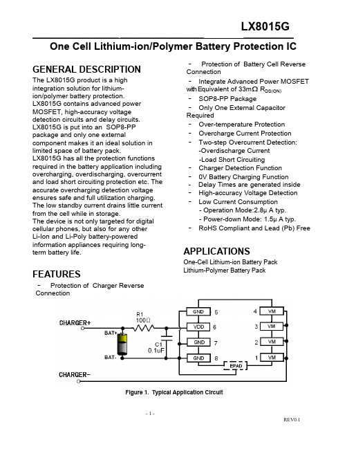
LX8015G ______________________________________ _____________________________________ ______________________ One Cell Lithium-ion/Polymer Battery Protection ICGENERAL DESCRIPTIONThe LX8015G product is a high integration solution for lithium-ion/polymer battery protection.LX8015G contains advanced power MOSFET, high-accuracy voltage detection circuits and delay circuits.LX8015G is put into an SOP8-PP package and only one external component makes it an ideal solution in limited space of battery pack.LX8015G has all the protection functions required in the battery application including overcharging, overdischarging, overcurrent and load short circuiting protection etc. The accurate overcharging detection voltage ensures safe and full utilization charging. The low standby current drains little current from the cell while in storage.The device is not only targeted for digital cellular phones, but also for any otherLi-Ion and Li-Poly battery-powered information appliances requiring long-term battery life.FEATURES·Protection of Charger Reverse Connection·Protection of Battery Cell Reverse Connection·Integrate Advanced Power MOSFET with Equivalent of 33mΩ R DS(ON)·SOP8-PP Package·Only One External Capacitor Required·Over-temperature Protection ·Overcharge Current Protection ·Two-step Overcurrent Detection: -Overdischarge Current-Load Short Circuiting·Charger Detection Function·0V Battery Charging Function- Delay Times are generated inside ·High-accuracy Voltage Detection ·Low Current Consumption- Operation Mode:2.8μA typ.- Power-down Mode: 1.5μA typ. ·RoHS Compliant and Lead (Pb) FreeAPPLICATIONSOne-Cell Lithium-ion Battery PackLithium-Polymer Battery PackFigure 1. Typical Application CircuitORDERING INFORMATIONNote: “YW” is manufacture date code, “Y” means the year, “W” means the weekPIN CONFIGURATIONFigure 2. PIN ConfigurationPIN DESCRIPTIONABSOLUTE MAXIMUM RATINGS(Note: Do not exceed these limits to prevent damage to the device. Exposure to absolute maximum rating conditions for long periods may affect device reliability.)ELECTRICAL CHARACTERISTICSTypicals and limits appearing in normal type apply for T A= 25o C, unless otherwise specifiedFigure 3. Functional Block Diagram FUNCTIONAL DESCRIPTIONThe LX8015G monitors the voltage andcurrent of a battery and protects it frombeing damaged due to overcharge voltage,overdischarge voltage, overdischarge current, and short circuit conditions by disconnecting the battery from the load or charger. These functions are required in order to operate the battery cell within specified limits.The device requires only one external capacitor. The MOSFET is integrated and its R DS(ON) is as low as33mΩtypical. Normal operating modeIf no exception condition is detected, charging and discharging can be carried out freely. This condition is called the normal operating mode.Overcharge ConditionWhen the battery voltage becomes higher than the overcharge detection voltage (V CU)during charging under normal condition and the state continues for the overcharge detection delay time (t CU) or longer, theLX8015G turns the charging control FET off to stop charging. This condition is called the overcharge condition. The overcharge condition is released in the following two cases:1, When the battery voltage drops below the overcharge release voltage (V CL), the LX8015G turns the charging control FET on and returns to the normal condition.2, When a load is connected and discharging starts, the LX8015G turns the charging control FET on and returns to the normal condition. The release mechanism is as follows: the discharging current flows through an internal parasitic diode of the charging FET immediately after a load is connected and discharging starts, and the VM pin voltage increases about 0.7 V (forward voltage of the diode) from the GND pin voltage momentarily. TheLX8015G detects this voltage and releases the overcharge condition. Consequently, in the case that the battery voltage is equal to or lower than the overcharge detection voltage (V CU), the LX8015G returns to the normal condition immediately, but in the case the battery voltage is higher than the overcharge detection voltage (V CU),the chip does not return to the normal condition until the battery voltage drops below the overcharge detection voltage (V CU) even if the load is connected. In addition, if the VM pin voltage is equal to or lower than the overcurrent detection voltage when a load is connected and discharging starts, the chip does not return to the normal condition.Remark If the battery is charged to a voltage higher than the overcharge detection voltage (V CU) andthe battery voltage does not drops below the overcharge detection voltage (V CU) even when a heavy load, which causes an overcurrent, is connected, the overcurrent do not work until the battery voltage drops below the overcharge detection voltage (V CU). Since an actual battery has, however, an internal impedance of several dozensof mΩ, and the battery voltage drops immediately after a heavy load which causes an overcurrent is connected, the overcurrent work. Detection of load short-circuiting works regardless of the battery voltage.Overdischarge ConditionWhen the battery voltage drops below the overdischarge detection voltage (V DL) during discharging under normal condition and it continues for the overdischarge detection delay time (t DL) or longer, theLX8015G turns the discharging controlFET off and stops discharging. This condition is called overdischarge condition. After the discharging control FET is turned off, the VM pin is pulled up by the R VMD resistorbetween VM and VDD in LX8015G. Meanwhile when VM is bigger than 1.5V (typ.) (the load short-circuiting detection voltage), the current of the chip is reduced to the power-down current (I PDN). This condition is called power-down condition. The VM and VDD pins are shorted by theR VMD resistor in the IC under the overdischarge and power-down conditions. The power-down condition is released when a charger is connected and the potential difference between VM and VDD becomes 1.3 V (typ.) or higher (load short-circuiting detection voltage). At this time, the FET is still off. When the battery voltage becomes the overdischarge detection voltage (V DL) or higher (see note), the LX8015G turns the FET on and changes to the normal condition from the overdischarge condition.Remark If the VM pin voltage is no less than the charger detection voltage (V CHA), when the battery under overdischarge condition is connected to a charger, the overdischarge condition is released (the discharging control FET is turned on) as usual, provided that the battery voltage reaches the overdischarge release voltage (V DU) or higher. Overcurrent ConditionWhen the discharging current becomes equal to or higher than a specified value (the VM pin voltage is equal to or higher than the overcurrent detection voltage) during discharging under normal condition and the state continues for the overcurrent detection delay time or longer, theLX8015G turns off the discharging control FET to stop discharging. This condition is called overcurrent condition. (The overcurrentincludes overcurrent, or load short-circuiting.)The VM and GND pins are shorted internally by the R VMS resistor under the overcurrent condition. When a load is connected, the VM pin voltage equals the VDD voltage due to the load.The overcurrent condition returns to the normal condition when the load is released and the impedance between the B+ and B- pins becomes higher than the automatic recoverable impedance. When the load is removed, the VM pin goes back to the GND potential since the VM pin is shorted the GND pin with the R VMS resistor. Detecting that the VM pin potential is lower than the overcurrent detection voltage(V IOV1), the IC returns to the normal condition.Abnormal Charge Current DetectionIf the VM pin voltage drops below the charger detection voltage (V CHA) during charging under the normal condition and it continues for the overcharge detection delay time (t CU) or longer, the LX8015G turns the charging control FET off and stops charging. This action is called abnormal charge current detection. Abnormal charge current detection works when the discharging control FET is on and the VM pin voltage drops below the charger detection voltage (V CHA). When an abnormal charge current flows into a battery in the overdischarge condition, the LX8015G consequently turns the charging control FET off and stops charging afterthe battery voltage becomes the overdischarge detection voltage and the overcharge detection delay time (t CU) elapses.Abnormal charge current detection is released when the voltage difference between VM pin and GND pin becomes lower than the charger detection voltage (V CHA) by separating the charger. Since the 0 V battery charging function has higher priority than the abnormal charge current detection function, abnormal charge current may not be detected by the product with the 0 V battery charging function while the battery voltage is low.Load Short-circuiting conditionIf voltage of VM pin is equal or below short circuiting protection voltage (V SHORT), the LX8015G will stop discharging and battery is disconnected from load. The maximum delay time to switch current off is t SHORT. This status is released when voltage of VM pin is higher than short protection voltage (V SHORT), such as when disconnecting the load.Delay CircuitsThe detection delay time for overdischarge current 2 and load short-circuiting starts when overdischarge current 1 is detected. As soon as overdischarge current 2 or load short-circuiting is detected over detection delay time for overdischarge current 2 or load short- circuiting, the LX8015G stops discharging. When battery voltage falls below overdischarge detection voltage due to overdischarge current, the LX8015G stop discharging by overdischarge current detection. In this case the recovery of battery voltage is so slow that if battery voltage after overdischarge voltage detection delay time is still lower than overdischargedetection voltage, the LX8015G shifts to power-down.Figure 4. Overcurrent delay time0V Battery Charging Function (1) (2) (3) This function enables the charging of a connected battery whose voltage is 0 V by self-discharge. When a charger having 0 V battery start charging charger voltage(V0CHA) or higher is connected between B+ and B- pins, the charging control FET gate is fixed to VDD potential. When the voltage between the gate and the source of the charging control FET becomes equal to or higher than the turn-on voltage by the charger voltage, the charging control FET is turned on to start charging. At this time, the discharging control FET is off and the charging current flows through the internal parasitic diode in the discharging control FET. If the battery voltage becomes equal to or higher than the overdischarge release voltage (V DU), the normal condition returns. Note(1) Some battery providers do not recommend charging of completely discharged batteries. Please refer to battery providers before the selection of 0 V battery charging function.(2) The 0V battery charging function has higher priority than the abnormal charge current detection function. Consequently, a product with the 0 V battery charging function charges a battery and abnormal charge current cannot be detected during the battery voltage is low (at most 1.8 V or lower).(3) When a battery is connected to the IC for the first time, the IC may not enter the normal condition in which discharging is possible. In this case, set the VM pin voltage equal to the GND voltage (short the VM and GND pins or connect a charger) to enter the normal condition.TIMING CHART 1.Overcharge and overdischarge detectionV V CU -V V DL +V V DL ONONCHARGEV DDV ov1V SS V VMFigure5-1 Overcharge and Overdischarge Voltage Detection2.Overdischarge current detectionV CU V CU -V HC V DL +V DH V DLONDISCHARGEOFFV DDV V ov2V ov1V SS(1)(4)(1)(1)(1)(4)(4)Figure5-2 Overdischarge Current DetectionRemark: (1) Normal condition (2) Overcharge voltage condition (3) Overdischarge voltage condition (4)Overcurrent condition3. Charger DetectionVV CU-VV DL+VV DLONV DDVMV SSVFigure5-3 Charger Detection4.Abnormal Charger DetectionVV CU-VV DL+VV DLONONCHARGEV DDVMV SSVFigure5-4 Abnormal Charger DetectionRemark: (1) Normal condition (2) Overcharge voltage condition (3) Overdischarge voltage condition (4)Overcurrent condition)TYPICAL APPLICATIONAs shown in Figure 6, the bold line is the high density current path which must be kept as short as possible. For thermal management, ensure that these trace widths are adequate. C is a decoupling capacitor which should be placed as close as possible to LX8015G.Fig 6 LX8015G in a Typical Battery Protection CircuitPrecautions• Pay attention to the operating conditions for input/output voltage and load current so that the power loss in LX8015G does not exceed the power dissipation of the package.• Do not apply an electrostatic discharge to this LX8015G that exceeds the performance ratings of the built-in electrostatic protection circuit.LX8015G ______________________________________ ____________________________________________ ________ ___________ - 11 -REV0.1 PACKAGE OUTLINE SOP8-EPAD PACKAGE OUTLINE AND DIMENSIONSIn order to increase the driver current capability of LX8015G and improve the temperature of package, Please ensure Epad and enough ground PCB to release energy.。
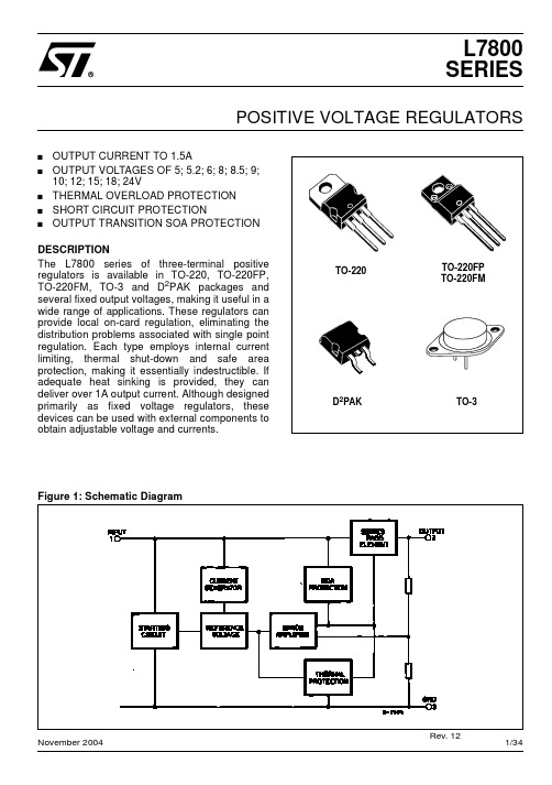
L7805CD2T-TR中文资料
- 1、下载文档前请自行甄别文档内容的完整性,平台不提供额外的编辑、内容补充、找答案等附加服务。
- 2、"仅部分预览"的文档,不可在线预览部分如存在完整性等问题,可反馈申请退款(可完整预览的文档不适用该条件!)。
- 3、如文档侵犯您的权益,请联系客服反馈,我们会尽快为您处理(人工客服工作时间:9:00-18:30)。
SHDN/RT GND LX PGND 2 3 8 GND 9 6 4 5 7 COMP FB VDD PVDD
Ordering Information
RT8015 Package Type SP : SOP-8 (Exposed Pad-Option 2) Lead Plating System P : Pb Free G : Green (Halogen Free and Pb Free)
Features
l l l l l l l l
High Efficiency : Up to 95% Low RDS(ON) Internal Switches : 110mΩ Programmable Frequency : 300kHz to 2MHz No Schottky Diode Required 0.8V Reference Allows Low Output Voltage Forced Continuous Mode Operation Low Dropout Operation : 100% Duty Cycle RoHS Compliant and 100% Lead (Pb)-Free
Applications
l l l l l l
Portable Instruments Battery-Powered Equipment Notebook Computers Distributed Power Systems IP Phones Digital Cameras
Pin Configurations
FB 7 COMP 8
1 SHDN/RT
GND 2, Exposed Pad (9)
Note : Using all Ceramic Capacitors Recommended Component for Different Output Voltage Applications
VOUT 3.3V 2.5V 1.8V 1.2V
L1 (uH) COUT (uF) 2.2 2.2 1.0 1.0 22 22 22 22
R1 (kΩ) 750 510 300 120
R2 (kΩ) 240 240 240 240
RCOMP (kΩ) CCOMP (nF) 13 13 7.5 7.5 1 1 1.5 1.5
Functional Pin Description
Note : Richtek products are :
}
SOP-8 (Exposed Pad)
RoHS compliant and compatible with the current requirements of IPC/JEDEC J-STD-020. Suitable for use in SnPb or Pb-free soldering processes.
Int-SS 0.9V 0.7V Control Leabharlann ogicDriver LX
NISEN POR 0.4V NMOS I Limit
PGND
VREF
OTP
GND
VDD
DS8015-03 March 2011
3
RT8015
Operation
Main Control Loop The RT8015 is a monolithic, constant-frequency, current mode step-down DC/DC converter. During normal operation, the internal top power switch (P-Channel MOSFET) is turned on at the beginning of each clock cycle. Current in the inductor increases until the peak inductor current reach the value defined by the voltage on the COMP pin. The error amplifier adjusts the voltage on the COMP pin by comparing the feedback signal from a resistor divider on the FB pin with an internal 0.8V reference. When the load current increases, it causes a reduction in the feedback voltage relative to the reference. The error amplifier raises the COMP voltage until the average inductor current matches the new load current. When the top power MOSFET shuts off, the synchronous power switch (N-Channel MOSFET) turns on until either the bottom current limit is reached or the beginning of the next clock cycle. The operating frequency is set by an external resistor connected between the RT pin and ground. The practical switching frequency can range from 300kHz to 2MHz. Power Good comparators will pull the PGOOD output low if the output voltage comes out of regulation by 12.5%. In an over-voltage condition, the top power MOSFET is turned off and the bottom power MOSFET is switched on until either the over-voltage condition clears or the bottom MOSFET's current limit is reached. Frequency Synchronization The internal oscillator of the RT8011 can be synchronized to an external clock connected to the SYNC pin. The frequency of the external clock can be in the range of 300kHz to 2MHz. For this application, the oscillator timing resistor should be chosen to correspond to a frequency that is about 20% lower than the synchronization frequency. Dropout Operation When the input supply voltage decreases toward the output voltage, the duty cycle increases toward the maximum on-time. Further reduction of the supply voltage forces the main switch to remain on for more than one cycle eventually reaching 100% duty cycle.
2, 9 (Exposed Pad) 3 4 5 6 7
GND
LX PGND PVDD VDD FB
2
DS8015-03 March 2011
RT8015
Function Block Diagram
SHDN/RT
SD ISEN OSC COMP 0.8V FB EA Output Clamp OC Limit Slope Com PVDD
}
DS8015-03 March 2011
1
RT8015
Typical Application Circuit
RT8015 VIN 2.6V to 5.5V CIN 22uF ROSC 332k 5 PVDD 6 VDD 4 PGND LX 3 L1 2.2uH R1 510k RCOMP 13k CCOMP 1nF R2 240k COUT 22uF VOUT 2.5V/2A
Pin No. 1 Pin Name SHDN/RT Pin Function Oscillator Resistor Input. Connecting a resistor to ground from this pin sets the switching frequency. Forcing this pin to VDD causes the device to be shut down. Signal Ground. All small-signal components and compensation components should connect to this ground, which in turn connects to PGND at one point. The exposed pad must be soldered to a large PCB and connected to GND for maximum power dissipation. Internal Power MOSFET Switches Output. Connect this pin to the inductor. Power Ground. Connect this pin close to the (−) terminal of CIN and COUT. Power Input Supply. Decouple this pin to PGND with a capacitor. Signal Input Supply. Decouple this pin to GND with a capacitor. Normally V DD is equal to PVDD. Feedback Pin. Receives the feedback voltage from a resistive divider connected across the output. Error Amplifier Compensation Point. The current comparator threshold increases 8 COMP with this control voltage. Connect external compensation elements to this pin to stabilize the control loop.