SD103AWS-V中文资料
SD103AX中文资料
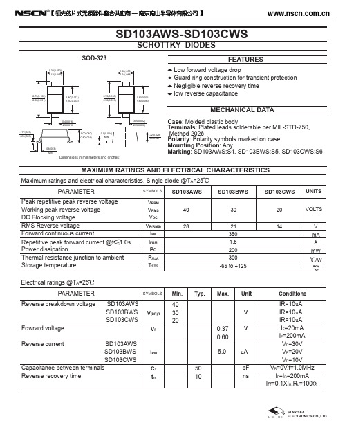
FEATURES
Low Forward Voltage Drop Guard Ring Construction for Transient Protection Low Reverse Recovery Time Low Reverse Capacitance
0.5~0.7
SOD-523
0.07~0.2
VALUES
40 28 350 1 150 300 125, -65~125
UNITS
V V mA A mW ℃/W ℃
ELECTRICAL RATINGS (Rating 25°C ambient temperature unless otherwise specified) PARAMETERS SYMBOL TEST CONDITIONS
1.5~1.7 0.15~0.25
MARKING:
S4
0.7~0.9
0.1~0.3 1.1~1.3
Dimensions in millimeters
The markUM RATINGS AND ELECTRICAL CHARACTERISTICS (Single diode, rating 25°C ambient temperature unless otherwise specified) TYPE NUMBER SYMBOL
MICRO SD 3.0 SPEC
MicroSD3.0 UHS-I SpecificationRev B2Sep-23-2014NOTE: INFORMATION IN THIS PRODUCT SPECIFICATION IS SUBJECT TO CHANGE AT ANYTIME WITHOUT NOTICE, ALL PRODUCT SPECIFICATIONS ARE PROVIDED FOR REFERENCE ONLY.TO ANY INTELLECTUAL, PROPERTY RIGHTS IN LONGSYS ELECTRONICS CO.,LTD. ALL INFORMATION IN THIS DOCUMENT IS PROVIDED.Contents1. Overview (4)1.1 Product Description (4)1.2 Features Summary (4)2. Pin Assignment (5)3. Product List (5)4. Current Consumption (7)5. Operational Environment (7)6. Card Registers (7)6.1 Card Identification Register (CID) (7)6.2 Card-Specific Data Register (CSD) (8)7. Bus Operation Conditions (9)7.1 For 3.3V Signaling (9)7.1.1 Threshold Level for High Voltage Range (9)7.1.2 Peak Voltage and Leakage Current (9)7.1.3 Bus Signal Line Load (10)7.1.4 Bus Signal Levels (10)7.1.5 Bus Timing(Default) (10)7.1.6 Bus Timing(High-Speed Mode) (12)7.2 For 1.8V Signaling (13)7.2.1 Threshold Level for High Voltage Range (13)7.2.2 Peak Voltage and Leakage Current (13)7.2.3 Bus Timing Specification in SDR12 (13)7.2.3.1 Clock Timing (14)7.2.3.2 Card Input Timing (14)7.2.3.3 Card Output Timing (14)7.2.3.3.1 Output Timing of Fixed Data Window (15)7.2.3.3.2 Output Timing of Variable Window (SDR104) (15)8. Physical Dimension (15)1. Overview1.1 Product DescriptionThe Longsys MicroSD3.0 Cards are fully compatible with Physical Layer Specification, Version 3.0 (this specification is available from the SDA), support Ultra High Speed(UHS), provides high write/read speed and high IOPS, It was designed to meet the security, high capacity, high performance and environmental requirements inherent in next generation consumer electronic devices.The MicroSD3.0 card system is a new mass-storage system based on innovations in semiconductor technology. It has been developed to provide an inexpensive, mechanically robust storage medium in card form for multimedia consumer applications. MicroSD card allows the design of inexpensive players and drivers without moving parts. A low power consumption and a wide supply voltagerange favors consumer electronic devices.Ultra High Speed (UHS) CardIt provides up to 104MB/s* performance. UHS cards are backward compatible on non-UHS hosts. *Based on internal testing; performance may vary depending upon host device.1 megabyte(MB)=1,000,000bytes.1.2 Features Summary-Capacity: 4GB/8GB/16GB/32GB/64GB/128GB-Complies to SD specifications version 3.00-Voltage operating: 2.7~3.6V.-Targeted for portable and stationary applications-Greater Performance Choices-Bus Speed Mode:DS-Default Speed mode: 3.3V signaling, frequency up to 25MHz, up to 12.5MB/secHS-High Speed mode: 3.3V signaling, frequency up to 50MHz, up to 25MB/secSDR12-1.8V signaling, frequency up to 25MHz, up to 12.5MB/secSDR25-1.8V signaling, frequency up to 50MHz, up to 25MB/secSDR50-1.8V signaling, frequency up to 100MHz, up to 50MB/secSDR104-1.8V signaling, frequency up to 208MHz, up to 104MB/secDDR50-1.8V signaling, frequency up to 50MHz, sampled on both clock edges, up to 50MB/s-Switch function command supports Bus Speed Mode, Command System, Drive Strength, and future functions.-password protection (CMD42-LOCK_UNLOCK)-Sophisticated system for error recovery including a powerful ECC-Global Wear Leveling-Power management for low power operation-Add TF card adapter can be used in SD card socket.2. Pin AssignmentPin No.SD ModeName Type Description 1 Dat2 I/O/PP Data Line [Bit 2]2CD/DAT3I/O/PP3Card Detect / Data Line [Bit 3]3 CMD PP Command/Response4 VDD S Supply voltage5 CLK I Clock6 VSS S Supply voltage ground7 DAT0 I/O/PP Data Line [Bit 0] 8DAT1I/O/PPData Line [Bit 1]S: power supply; I: input; O: output; PP: I/O using push-pull driversTable 1: Pin Assignment3. Product ListPart NumberCapacityActual Size(Min ) (note2)Speed Class (note1) Write Speed (Typical) (note1) UHS-I (note1)TypeNCIX4XX-004G 4GB 3.6GB Class4 4 MB/S SDR50/SDR104 SDHC NCIX6XX-004G 4GB 3.6GB Class6 6 MB/S SDR50/SDR104 SDHC NCIXAXX-004G 4GB 3.6GB Class10 10 MB/S SDR50/SDR104 SDHC NCIX4XX-008G 8GB 7.3GB Class4 4 MB/S SDR50/SDR104 SDHC NCIX6XX-008G8GB7.3GBClass66 MB/SSDR50/SDR104SDHCNCIXAXX-008G 8GB 7.3GB Class10 10 MB/S SDR50/SDR104 SDHC NCIXBXX-008G 8GB 7.3GB Class10 133X SDR104 SDHC NCIXCXX-008G 8GB 7.3GB Class10 150X SDR104 SDHC NCIXAXX-016G 16GB 14.7GB Class10 10 MB/S SDR50/SDR104 SDHC NCIXBXX-016G 16GB 14.7GB Class10 133X SDR104 SDHC NCIXCXX-016G 16GB 14.7GB Class10 150X SDR50/SDR104 SDHC NCIXDXX-016G 16GB 14.7GB Class10 233X SDR104 SDHC NCIXEXX-016G 16GB 14.7GB Class10 266X SDR104 SDHC NCIXFXX-016G 16GB 14.7GB Class10 300X SDR104 SDHC NCIXAXX-032G 32GB 29.4GB Class10 10 MB/S SDR50/SDR104 SDHC NCIXBXX-032G 32GB 29.4GB Class10 133X SDR104 SDHC NCIXCXX-032G 32GB 29.4GB Class10 150X SDR104 SDHC NCIXDXX-032G 32GB 29.4GB Class10 233X SDR50/SDR104 SDHC NCIXEXX-032G 32GB 29.4GB Class10 266X SDR104 SDHC NCIXFXX-032G 32GB 29.4GB Class10 300X SDR104 SDHC NCIXGXX-032G 32GB 29.4GB Class10 333X SDR104 SDHC NCIXHXX-032G 32GB 29.4GB Class10 400X SDR104 SDXC NCIXAXX-064G 64GB 58.9GB Class10 10 MB/S SDR50/SDR104 SDXC NCIXHXX-064G 64GB 58.9GB Class10 333X SDR104 SDXC NCIXHXX-064G 64GB 58.9GB Class10 400X SDR104 SDXC NCIXBXX-128G 128GB 118GB Class10 150X SDR104 SDXCTable 2: Product Listnote1:*Measurement based on VTE3100 TestMetrix device, SW 3.2A software or up version, test script:SD_Card(Spec3.0_High&Extended-Capacity_UHS-I and Non-UHS-I)_Compliance [rev31R].vte*SDR50@SDR50-100MHzSDR104@SDR104-208MHz.*1X=150KByte/snote2: *1Gigabyte (GB) = 1 billion bytes. Some capacity not available for data storage*Maximum speed differs from the bus I/F speed. It varies depending upon the card performance. The average speed that a device writes to a MicroSD memory card may vary depending upon the device and the operation it is performing. The speed may also depend on how other data is stored on the MicroSD memory card. Normal and high-speed cards can also be used with UHS-I host devices, but the high performance enabled by a UHS-I host device can only be achieved with a UHS-I memory card.4. Current ConsumptionStandby current: 500uA(Maximum value)Standby current: 150uA(average value)Operating current: 250mA(Maximum value)Operating current: 100mA(average value)*Test condition: Realtek5308 card reader (Voltage 3.3V), Fluke289C multi-meter.5. Operational EnvironmentParameter RangeTemperatureOperating 0℃~ 70℃Non-Operating -40℃~ 85℃HumidityOperating 25% to 85%, non-condensing Non-Operating 25% to 85%, non-condensingDurability insertion/removal cycles 10,000 Data Retention10yearsTable 3: Operational Environment6. Card Registers6.1 Card Identification Register (CID)The Card Identification (CID) register is 128 bit wide. It contains the card identification information used during the card identification phase. Every individual flash card shall have a unique identification number.The structure of the CID register is defined in the following table.CID Bit Width Name Field[127:120] 8 ManufactureID MID [119:104] 16 OEM/ApplicationID OID [103:64] 40 ProductName PNM [63:56] 8 ProductRevision PRV [55:24] 32 Product Serial Number PSN[23:20] 4 Reserved ---[19:8] 12 ManufacturingDate MDT [7:1] 7 CRC7 check sum CRC[0] 1 Notused,always”1 ---Table 4: CID Table- All contents in the CID table are programmable; Manufacturers can update the CID data through utility.- Manufacturers should license MID and OID field form the SD Card Association(SDA)6.2 Card-Specific Data Register (CSD)The Card-Specific Data register provides information on how to access the card contents. The defines the data format, error correction type, maximum data access time, data transfer speed, whether the DSR register can be used etc. The programmable part of the register can be changed by CMD27.The CSD Table Version 2.0(as shown below) is applied to SDHC and SDXC Cards. Note that bits [15:0] are programmable by the host side. Refer to the SD specification for detailed information CSD BitWidth NameFieldValueNote [127:126] 2 CSD structureCSD_STRUCTURE 01bV2.0(>2GB Card) [125:120] 6 Reserved --- --- --- [119:112]8Data read access-time 1 (TAAC)0E h[111:104] 8 Data read access-time2 in CLK cycles(NSA*100)(NSAC) 00 h[103:96] 8 Max data transfer rate (TRAN_SPEED)32 h5A h 0B h 2B h[95:84] 12 Card command classes CCC5B5 h[83:80] 4 Max. read data block length (READ_BL_LEN) 9 h 512 Byte[79] 1 Partial block read allowed (READ_BL_PARTIA L)[78]1Write block misalignment(WRITE_BLK_MISA LIGN)[77] 1 Read block misalignment(READ_BLK_MISAL IGN) 0[76] 1 DSR implemented DSR_IMP x[75:70] 6 Reserve --- --- [69:48] 22 Device size C_SIZE xxxxxxh[47] 1 Reserved --- 0 [46] 1 Erase single block enable (ERASE_BLK_EN) 1[45:39] 7 Erase sector size (SECTOR_SIZE) 7F h [38:32] 7 Write protect group size C_SIZE0 b[31] 1 Write protect group enable --- 0 [30:29] 2 Reserved(ERASE_BLK_EN) 0 b [28:26] 3 Write speed factor(SECTOR_SIZE)010 b [25:22]4Max. write data block (WP_GRP_SIZE)9 hlength[21] 1 Partial block write allowed (WP_GRP_ENABLE)[20:16] 5 Reserved --- ---[15] 1Fileformatgroup (FILE_FORMAT_GRP)[14] 1Copyflag COPY x[13] 1Permanentwriteprotection PERM_WRITE_PROTECTx[12] 1 Temporary write protection TMP_WRITE_PROTECTx[11:10] 2 File format (FILE_FORMAT) 00 b[9:8] 2 Reserved --- 00b[7:1] 7 CRC CRC ---[0] 1Notused,always’1’ --- 1Table 5: CSD (Version 2.0) Table7. Bus Operation Conditions7.1 For 3.3V Signaling7.1.1 Threshold Level for High Voltage RangeParameter Symbol Min Max Unit Remark Supply Voltage V DD 2.7 3.6 VOutput High Voltage V OH 0.75*V DD V I OH=2mA V DD min Output Low Voltage V OL0.125*V DD V I OL=2mA V DD min Input High Voltage V IH 0.625*V DD V DD+0.3 VInput Low Voltage V IL V ss-0.3 0.25*V DD VPower Up Time 250 ms From 0V to V DD minTable 6: Threshold Level for High Voltage7.1.2 Peak Voltage and Leakage CurrentParameter Symbol Min Max Unit Remark Peak voltage on all lines VAll InputsInput Leakage Current -10 10 uAAll OutputsOutput Leakage Current -10 10 uATable 7: Peak Voltage and Leakage Current7.1.3 Bus Signal Line LoadParameter SymbolMin Max Unit RemarkPull-up resistance R CMDR DAT10 100 KΏTo prevent bus floatingTotal bus capacitance for each signal line C L40 pF1 card C HOST+C BUS shall notexceed 30pFCard capacitance foreach signal pinC CARD10 pFMaximum signalinductance16 nHPull-up resistance insidecard(pin1)R DAT3 10 90 KΏMay be used for card detectionCapacity Connected toPower Line C C 5 uF To prevent inrush currentTable 8: Bus Operating Conditions - Signal Line's Load7.1.4 Bus Signal LevelsAs the bus can be supplied with a variable supply voltage,all sigelnal levels are related to the supply valtage.Figure 1: Bus Signal LevelsTo meet the requirements of the the JEDEC specification JESD8-1A and JESD8-7,the card input and output voltages shall be within the specifide ranges shown in Table 6 for any V DD of the allowed valtage range.7.1.5 Bus Timing(Default)Figure 2:Card input Timing(Default Speed Card)Figure 3:Card Output Timing(Default Speed Mode)Unit RemarkParameter Symbo Min. MaxClock CLK (All values are referred to min(V IH)and max(V IL))Clock frequency data transfer fpp 0 25 MHz C≤ 10pF (1 card)CARDClock frequency Identification f0(1)/100 400 KHz C CARD≤ 10pF (1 card)ODClock low time t WL 10 ns C CARD≤ 10pF (1 card) Clock high time t WH 10 ns C CARD≤ 10pF (1 card) Clock rise time t TLH10 ns C CARD≤ 10pF (1 card) Clock fall time t THL10 ns C CARD≤ 10pF (1 card) Inputs CMD, DAT (referenced to CLK)Input set-up time t ISU 5 ns C CARD≤ 10pF (1 card)Input hold time t TH 5 nsC CARD≤ 10pF (1 card) Outputs CMD, DAT (referenced to CLK)Output Delay time during Datat ODLY 0 14 ns C L≤ 40pF (1 card) Transfer ModeOutput Hold time t OH 0 50 ns C L≤ 40pF (1 card) (1)0 Hz means to stop the clock.The given minimum frequency range is for cases were continuesclock is required (refer to Chapter 4.4-Clock Control)Table 9:Bus Timing-Parameters Values (Default Speed)7.1.6 Bus Timing(High-Speed Mode)Figure 4: Card Input Timing(High Speed Card)Figure5: Card Output Timing(High Speed Mode)Parameter Symbo Min. Max Unit RemarkClock CLK (All values are referred to min(V IH)and max(V IL))Clock frequency data transfer fpp 0 50 MHz CCARD≤ 10pF (1 card) Clock low time t WL 7 ns C CARD≤ 10pF (1 card) Clock high time t WH 7 ns C CARD≤ 10pF (1 card) Clock rise time t TLH 3 ns C CARD≤ 10pF (1 card) Clock fall time t THL 3 ns C CARD≤ 10pF (1 card) Inputs CMD, DAT (referenced to CLK)Input set-up time t ISU 6 ns C CARD≤ 10pF (1 card) Input hold time t TH 2 nsC CARD≤ 10pF (1 card) Outputs CMD, DAT (referenced to CLK)Output Delay time during DataTransfer Modet ODLY14 ns C L≤ 40pF (1 card) Output Hold time t OH 2.5 ns C L≥ 15pF (1 card)Total System capacitance for each line1C L40 pF1card1)In order to satisty sever timing , host shall drive only one card.Table 10 :Bus Tinming – Parameters Values(High Speed)7.2 For 1.8V Signaling7.2.1 Threshold Level for High Voltage RangeParameter Symbol Min Max Unit Remark Supply Voltage V DD 2.7 3.6 VRegulator Voltage V DDIO 1.7 1.95 V Generated by V DD Output High Voltage V OH 1.4 V I OH=2mA V DD min Output Low Voltage V OL0.45 V I OL=2mA V DD min Input High Voltage V IH 1.27 2.0 VInput Low Voltage V IL V ss-0.3 0.58 VTable 11: Threshold Level for High Voltage7.2.2 Peak Voltage and Leakage CurrentParameter Symbol Min Max Unit Remark Input Leakage Current -2 2 uA DAT3 pull-up isdisconnectedTable 12: Peak Voltage and Leakage Current7.2.3 Bus Timing Specification in SDR12, SDR25, SDR50 and SDR104 Modes7.2.3.1 Clock TimingFigure 6: Clock Signal TimingSymbolMinMaxUnitRemarkt CLK 4.8 - ns208MHz (Max.), Between rising edge,V CT =0.975Vt CR , t CF - 0.2* t CLK nst CR , t CF < 2.00ns (max.) at 208MHz, C CARD =10pF t CR , t CF < 2.00ns (max.) at 100MHz, C CARD =10pFThe absolute maximum value of t CR , t CF is 10ns regardless of clock frequence. Clock Duty3070%Table 13:Clock Signal Timing7.2.3.2 Card Input TimingFigure 7: Card Input TimingSymbolMinMaxUnitSDR104 modet IS 1.40 - ns C CARD = 10pF , V CT = 0.975V t IH 0.80 ns C CARD = 5pF , V CT = 0.975V SymbolMinMaxUnitSDR12, SDR25 and SDR50 modest IS 3.00 - ns C CARD = 10pF , V CT = 0.975V t IH 0.80 - nsC CARD = 5pF , V CT = 0.975V Table 14: SDR50 and SDR104 Input Timing7.2.3.3 Card Output Timing7.2.3.3.1 Output Timing of Fixed Data Window (SDR12, SDR25 and SDR50)Figure 8:Output Timing of Fixed Date WindowSymbolMinMaxUnitRemarkt ODLY - 7.5 nst CLK ≥10.0ns, CL=30pF, using driver Type B,for SDR50. t ODLY 14 nst CLK ≥20.0ns, CL=40pF, using driver Type B,for SDR25 and SDR12. t OH1.5-nsHold time at the t ODLY (min.). CL=15pFTable 15: Output Timing of Fixed Data Window7.2.3.3.2 Output Timing of Variable Window (SDR104)Figure 9: Output Timing of Variable Data WindowSymbol Min Max Unit Remarkt OP -2UICard Output Phase△t OP-350 +1550 psDelay variation due to temperature change after tuningt ODW 0.60 - UIt ODW = 2.88ns at 208MHz Table 16: Output Timing of Variable Data Window8. Physical DimensionType MeasurementLength15mm+/-0.1mm(B)Width11mm+/-0.1mm(A)Thickness 1.0mm+/-0.1mm(C)0.7mm+/-0.1mm(C1)Weight 0.33gram MaxTable 17: MicroSD card physical dimension (Unit in mm) Mechanical form factor as follows: (Unit in mm)Figure 10: Bottom ViewFigure 11: TOP View。
SD103AWS-7-F;SD103BWS-7-F;SD103CWS-7-F;SD103AWS-7;SD103CWS-7;中文规格书,Datasheet资料

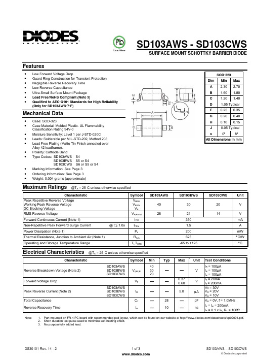
SURFACE MOUNT SCHOTTKY BARRIER DIODEFeatures• Low Forward Voltage Drop • Guard Ring Construction for Transient Protection • Negligible Reverse Recovery Time • Low Reverse Capacitance • Ultra-Small Surface Mount Package • Lead, Halogen and Antimony Free, RoHS Compliant "Green" Device (Notes 3 and 4) • Qualified to AEC-Q101 Standards for High Reliability (Only for SD103AWS-7-F)Mechanical Data• Case: SOD-323• Case Material: Molded Plastic. UL Flammability Classification Rating 94V-0• Moisture Sensitivity: Level 1 per J-STD-020D• Leads: Solderable per MIL-STD-202, Method 208 • Lead Free Plating (Matte Tin Finish annealed over Alloy 42 leadframe). • Polarity: Cathode Band• Marking Information: See Page 2 • Ordering Information: See Page 2 •Weight: 0.004 grams (approximate)Top ViewMaximum Ratings @T A = 25°C unless otherwise specifiedCharacteristicSymbol SD103AWSSD103BWSSD103CWSUnit Peak Repetitive Reverse Voltage Working Peak Reverse Voltage DC Blocking VoltageV RRM V RWM V R 40 30 20 V RMS Reverse VoltageV R(RMS)2821 14V Forward Continuous Current (Note 1)I FM 350 mA Non-Repetitive Peak Forward Surge Current @ t ≤ 1.0sI FSM1.5AThermal CharacteristicsCharacteristicSymbol Value Unit Power Dissipation (Note 1)P D 200 mW Thermal Resistance, Junction to Ambient Air (Note 1) R θJA 625 °C/W Operating and Storage Temperature Range T J, T STG-65 to +125°CElectrical Characteristics @T A = 25°C unless otherwise specifiedCharacteristic SymbolMin Typ Max Unit Test ConditionsSD103AWS Reverse Breakdown Voltage (Note 2) SD103BWS SD103CWS V (BR)R 4030 20 ⎯ ⎯ V I R = 100μA I R = 100μA I R = 100μAForward Voltage Drop V F⎯ ⎯ 0.370.60 V I F = 20mA I F = 200mASD103AWSPeak Reverse Current (Note 2) SD103BWS SD103CWS I R ⎯ ⎯ 5.0 μA V R = 30V V R = 20V V R = 10V Total Capacitance C T ⎯ 28 ⎯ pF V R = 0V, f = 1.0MHzReverse Recovery Time t rr⎯ 10 ⎯ ns I F = I R = 200mA,I rr = 0.1 x I R , R L = 100ΩNotes: 1. Part mounted on FR-4 PC board with recommended pad layout, which can be found on our website at /datasheets/ap02001.pdf. 2. Short duration test pulse used to minimize self-heating effect.3. No purposefully added lead. Halogen and Antimony Free.4. Product manufactured with Data Code V9 (week 33, 2008) and newer are built with Green Molding Compound. Product manufactured prior to Date CodeV9 are built with Non-Green Molding Compound and may contain Halogens or Sb 2O 3 Fire Retardants.Please click here to visit our online spice models database.0.010.110.0001I , I N S T A N T A N E O U S F O R W A R D C U R R E N T (A )F V , INSTANTANEOUS FORWARD VOLTAGE (mV)Fig. 1 Typical Forward Characteristics F0.010.11101001,0005101535302520V , INSTANTANEOUS REVERSE VOLTAGE (V)Fig. 2 Typical Reverse Characteristics R 4001051525203010203040V , DC REVERSE VOLTAGE (V)Fig. 3 Total Capacitance vs. Reverse Voltage R C , T O T A L C A P A C I T A N C E (p F )T0100255075100125P , P O W E R D I S S I P A T I O N (m W )D T , AMBIENT TEMPERATURE (C)Fig. 4 Power Derating CurveA °200Ordering Information (Note 5)Part Number Case Packaging SD103AWS-7-F SOD-323 3000/Tape & Reel SD103BWS-7-F SOD-323 3000/Tape & Reel SD103CWS-7-FSOD-3233000/Tape & ReelNotes: 5. For packaging details, go to our website at /datasheets/ap02007.pdf.Marking Informationxx = Product Type Marking Code S4 = SD103AWSS5 or S4 = SD103BWSS6 or S5 or S4 = SD103CWSXXPackage Outline DimensionsSuggested Pad LayoutIMPORTANT NOTICEDiodes Incorporated and its subsidiaries reserve the right to make modifications, enhancements, improvements, corrections or other changes without further notice to any product herein. Diodes Incorporated does not assume any liability arising out of the application or use of any product described herein; neither does it convey any license under its patent rights, nor the rights of others. The user of products in such applications shall assume all risks of such use and will agree to hold Diodes Incorporated and all the companies whose products are represented on our website, harmless against all damages.LIFE SUPPORTDiodes Incorporated products are not authorized for use as critical components in life support devices or systems without the expressed written approval of the President of Diodes Incorporated.SOD-323 Dim Min Max A 0.25 0.35 B 1.20 1.40 C 2.30 2.70 H 1.60 1.80 J 0.00 0.10 K 1.0 1.1 L0.20 0.40 M 0.10 0.15α0° 8°All Dimensions in mmDimensions Value (in mm)Z 3.75 G 1.05 X 0.65Y1.35C2.40分销商库存信息:DIODESSD103AWS-7-F SD103BWS-7-F SD103CWS-7-F SD103AWS-7SD103CWS-7SD103BWS-7。
SD103CWS-7-F中文资料
SD103AWS - SD103CWSSURFACE MOUNT SCHOTTKY BARRIER DIODEFeatures• Low Forward Voltage Drop• Guard Ring Construction for Transient Protection • Negligible Reverse Recovery Time • Low Reverse Capacitance• Ultra-Small Surface Mount Package • Lead Free/RoHS Compliant (Note 3)•Qualified to AEC-Q101 Standards for High Reliability (Only for SD103AWS-7-F)Mechanical Data• Case: SOD-323• Case Material: Molded Plastic. UL Flammability Classification Rating 94V-0• Moisture Sensitivity: Level 1 per J-STD-020C• Leads: Solderable per MIL-STD-202, Method 208 • Lead Free Plating (Matte Tin Finish annealed over Alloy 42 leadframe). • Polarity: Cathode Band•Type Codes: SD103AWS S4 SD103BWS S5 or S4 SD103CWS S6 or S5 or S4 • Marking Information: See Page 3 •Ordering Information: See Page 3 •Weight: 0.004 grams (approximate)SOD-323 Dim Min Max A 2.30 2.70 B 1.60 1.80 C 1.20 1.40 D 1.05 TypicalE 0.25 0.35 G 0.20 0.40 H 0.10 0.15 J 0.05 Typicalα0°8°All Dimensions in mmMaximum Ratings @T A = 25°C unless otherwise specifiedCharacteristicSymbol SD103AWSSD103BWSSD103CWSUnit Peak Repetitive Reverse Voltage Working Peak Reverse Voltage DC Blocking Voltage V RRM V RWM V R 40 30 20 V RMS Reverse VoltageV R(RMS) 2821 14V Forward Continuous Current (Note 1) I FM 350 mA Non-Repetitive Peak Forward Surge Current @ t ≤ 1.0sI FSM 1.5 A Power Dissipation (Note 1)P d 200 mW Thermal Resistance, Junction to Ambient Air (Note 1) R θJA 625 °C/W Operating and Storage Temperature RangeT j, T STG-65 to +125°CElectrical Characteristics @T A = 25°C unless otherwise specifiedCharacteristicSymbolMinTypMaxUnitTest ConditionsSD103AWS Reverse Breakdown Voltage (Note 2) SD103BWS SD103CWS V (BR)R 4030 20 ⎯ ⎯V I R = 100µA I R = 100µA I R = 100µAForward Voltage Drop V F ⎯ ⎯0.37 0.60 V I F = 20mAI F = 200mASD103AWS Peak Reverse Current (Note 2) SD103BWS SD103CWS I R ⎯ ⎯5.0 µA V R = 30VV R = 20V V R = 10V Total Capacitance C T ⎯ 28 ⎯pF V R = 0V, f = 1.0MHz Reverse Recovery Time t rr ⎯ 10 ⎯ns I F = I R = 200mA,I rr = 0.1 x I R , R L = 100ΩNote: 1. Part mounted on FR-4 PC board with recommended pad layout, which can be found on our website at /datasheets/ap02001.pdf. 2. Short duration test pulse used to minimize self-heating effect.3. No purposefully added lead.Ordering Information (Note 4)Device Packaging ShippingSD103AWS-7-F SOD-323 3000/Tape & ReelSD103BWS-7-F SOD-323 3000/Tape & ReelSD103CWS-7-F SOD-323 3000/Tape & ReelNotes: 4. For Packaging Details, go to our website at /datasheets/ap02007.pdf.Marking InformationXX = Product Type Marking Code, See Page 1IMPORTANT NOTICEDiodes Incorporated and its subsidiaries reserve the right to make modifications, enhancements, improvements, corrections or other changes without further notice to any product herein. Diodes Incorporated does not assume any liability arising out of the application or use of any product described herein; neither does it convey any license under its patent rights, nor the rights of others. The user of products in such applications shall assume all risks of such use and will agree to hold Diodes Incorporated and all the companies whose products are represented on our website, harmless against all damages.LIFE SUPPORTDiodes Incorporated products are not authorized for use as critical components in life support devices or systems without the expressed written approval of the President of Diodes Incorporated.。
爱国者移动存储王3代(加速度感应安全型)
2-4 性能特点 .....................................................5
2-5 技术规格 ....................................................6
2-6 质量认证 ....................................................6
定。配合高速 USB2.0 接口和高品质,1 分钟可传输 1.3G 数据*。本产品由于具
有以上易用、安全的特性和体积小重量轻等特点,将带给您最佳的移动存储体
验。
* 本数据为爱国者实验室测试数据,用户使用时的实际速度因具体环境而不同
2-2 产品结构图
4
电源指示灯
独有黑晶凝尘标记
数据指示灯
*产品以包装内实物为准,如有改变恕不另行通知
第三章 安装说明 ................................................7
3-1 安装前注意事项 ..............................................7
3-2 Windows 98SE 下的安装过程 ....................................7
4. 速度快,移动存储王Ⅲ代的理论极限传输速率可达 480Mb/s,实际测试速 度也具有明显优势。使用顶级 USB-to-IDE 方案,传输数据安全稳定,兼 容性好。
5
5. 容量大,提供各种规格的存储容量,满足不同人士的移动存储需要。 6. 兼容性好,可同时在 USB1.1 与 USB2.0 接口下使用。 7. 携带轻便,体积小重量轻。 8. 数据可以长期保存,无须任何的特别保存环境,就可以长期的保留宝贵的
SD103AWS贴片肖特基二极管规格书
SD103AWS 40 28
SD103BWS 30 21 350 1.5 200 300 -65 to +125
SD103CWS 20 14
UNITS VOLTS V mA A mW /W
VRRM VRMS VDC VR(RMS) IFM IFRM Pd RΘJA TSTG
.72(0.028) .69(0.027)
.08(.003) MIN
Case: Molded plastic body Terminals: Plated leads solderable per MIL-STD-750, Method 2026 Polarity: Polarity symbols marked on case Mounting Position: Any Marking: SD103AWS:S4, SD103BWS:S5, SD103CWS:S6
Min.
Typ.
Max.
Unit
Conditions
V(BR)R VF
40 30 20 0.37 0.60 5.0 50 10
V V
Fowrard voltage Reverse current SD103AWS SD103BWS SD103CWS Capacitance between terminals Reverse recovery time
【 领先的片式无源器件整合供应商 — 南京南山半导体有限公司 】
RATINGS AND CHARACTERISTIC CURVES SD103AWS-SD103CWS
FIG. 1- TYPICAL FORWARD CHARACTERISTICS
1000 100
SD103AWS二极管选型资料 标记S4
10
20
30
40
REVERSE VOLTAGE V (V) R
250 200 150 100
50 0 0
Power Derating Curve
25
50
75
100
125
AMBIENT TEMPERATURE T (℃) a
CAPACITANCE BETWEEN TERMINALS C (pF)
T
D,Mar,2013
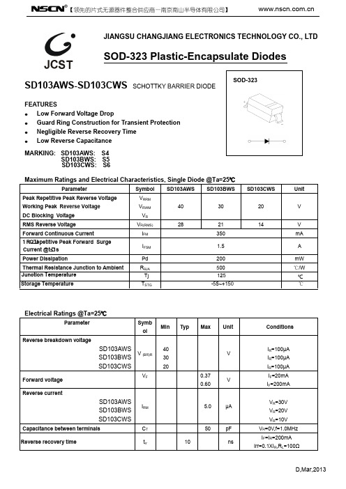
FEATURES z Low Forward Voltage Drop z Guard Ring Construction for Transient Protection z Negligible Reverse Recovery Time z Low Reverse Capacitance
MARKING: SD103AWS: S4 SD103BWS: S5 SD103CWS: S6
V
V mA A mW ℃/W ℃
℃
Electrical Ratings @Ta=25℃
Parameter
Symb Min Typ Max Unit
ol
Reverse br
SD103BWS V (BR)R 30
V
SD103CWS
20
Forward voltage
SOD-323 +
Maximum Ratings and Electrical Characteristics, Single Diode @Ta=25℃
Parameter
Symbol SD103AWS SD103BWS
Peak Repetitive Peak Reverse Voltage
LM103UPS电源专用说明书
一产品概述 (4)1.1LM103蓄电池在线监测装置的特点 (4)1.2主要用途及适用范围 (4)1.3LM103蓄电池在线监测装置的基本型号及配置 (4)1.5使用环境条件 (5)1.6安全 (5)二LM103蓄电池在线监测装置的结构特征与工作原理 (6)2.1总体结构及其工作原理 (6)2.2控制单元工作原理 (7)2.3采集模块 (7)2.4内阻模块 (7)三LM103蓄电池在线监测装置的技术特性 (8)3.1LM103蓄电池在线监测装置的主要功能 (8)3.2主要性能指标 (8)3.2.1性能指标 (8)3.2.2控制单元 (9)3.2.3采集模块 (9)3.2.4内阻模块 (9)四LM103蓄电池在线监测装置的外形及安装尺寸 (10)4.1控制单元 (10)4.2采集模块 (10)4.3内阻模块 (11)龙易电气4.4简易机架尺寸图 (11)五LM103蓄电池在线监测装置的安装调试 (13)5.1安装要求 (13)5.2安装程序、方法及注意事项 (13)5.3LM103蓄电池在线监测装置的试运行 (13)六LM103蓄电池在线监测装置使用前的注意事项 (14)6.1使用前的准备工作及注意事项 (14)6.2使用前及使用中的安全及安全防护 (14)七LM103蓄电池在线监测装置的使用、操作 (15)7.1熟悉界面 (15)7.1.1操作面板介绍 (15)7.1.2初始化主菜单 (15)7.1.3主要功能简介 (16)7.2系统参数设置 (17)7.2.1界面进入 (17)7.2.2参数说明 (17)7.2.3具体操作过程 (19)7.3实时监测功能 (21)7.3.1界面进入 (21)7.3.2参数与界面说明 (21)7.3.3操作介绍 (22)7.4实时报警查询 (23)7.4.1界面进入 (23)7.4.2界面介绍 (24)7.4.3操作简介 (24)7.5时间更改 (24)7.5.1进入界面 (24)7.5.2界面介绍 (25)7.5.3操作步骤 (25)7.6密码更改 (26)7.6.1操作简介 (26)八常见故障分析与排除 (27)8.1装置上指示灯说明 (27)8.2故障与排除 (27)九保养维护 (29)9.1运行时的维护 (29)9.2正常维修程序 (29)十运输与贮存时的注意事项 (29)10.1运输时的注意事项 (29)10.2贮存时注意事项 (29)十一服务与支持 (29)附录1产品的基础知识 (30)1.1蓄电池的相关概念 (30)1.2电池失效 (31)龙易电气1.3电池的日常维护 (32)1.4蓄电池检测方法 (33)1.5蓄电池检查 (33)非常感谢您采购和使用本产品,如在使用中出现疑问,欢迎来电咨询或登陆我们的网站:。
- 1、下载文档前请自行甄别文档内容的完整性,平台不提供额外的编辑、内容补充、找答案等附加服务。
- 2、"仅部分预览"的文档,不可在线预览部分如存在完整性等问题,可反馈申请退款(可完整预览的文档不适用该条件!)。
- 3、如文档侵犯您的权益,请联系客服反馈,我们会尽快为您处理(人工客服工作时间:9:00-18:30)。
SD103AWS-V/103BWS-V/103CWS-VDocument Number 85682Rev. 1.7, 18-Sep-06Vishay Semiconductors120145Small Signal Schottky DiodesFeatures•The SD103 series is a metal-on-silicon Schottky barrier device which is protectedby a PN junction guard ring•This diode is also available in theMini-MELF case with the type designations LL103A to LL103C, DO35 case with the type designations SD103A to SD103C and SOD123 case with type designations SD103AW-V to SD103CW-V•The low forward voltage drop and fast switching make it ideal for protection of MOS devices, steer-ing, biasing, and coupling diodes for fast switching and low logic level applications •For general purpose applications •Lead (Pb)-free component•Component in accordance to RoHS 2002/95/EC and WEEE 2002/96/ECMechanical DataCase: SOD323 Plastic case Weight: approx. 4.3 mgPackaging Codes/Options:GS18/10 k per 13" reel (8 mm tape), 10 k/box GS08/3 k per 7" reel (8 mm tape), 15 k/boxParts TableAbsolute Maximum RatingsT amb = 25°C, unless otherwise specified1) Valid provided that electrodes are kept at ambient temperatureThermal CharacteristicsT amb = 25°C, unless otherwise specified1) Valid provided that electrodes are kept at ambient temperaturePartOrdering codeT ype MarkingRemarks SD103AWS-V SD103AWS-V-GS18 or SD103AWS-V-GS08S6Tape and Reel SD103BWS-V SD103BWS-V-GS18 or SD103BWS-V-GS08S7Tape and Reel SD103CWS-VSD103CWS-V-GS18 or SD103CWS-V-GS08S8Tape and ReelParameterT est conditionPart Symbol Value Unit Peak reverse voltageSD103AWS-V V RRM 40V SD103BWS-V V RRM 30V SD103CWS-VV RRM 20V Power dissipation P tot 2001)mW Single cycle surge10 µs square waveI FSM2AParameterTest condition Symbol Value Unit Thermal resistance junction to ambient air R thJA 5001)K/W Junction temperature T j 1251)°C Storage temperature rangeT stg- 55 to + 1501)°C 2Document Number 85682Rev. 1.7, 18-Sep-06SD103AWS-V/103BWS-V/103CWS-VVishay Semiconductors Electrical CharacteristicsT amb = 25°C, unless otherwise specifiedTypical CharacteristicsT amb = 25 °C unless otherwise specifiedParameterT est conditionPart Symbol MinT yp.Max Unit Leakage currentV R = 30 V SD103AWS-V I R 5µA V R = 20 V SD103BWS-V I R 5µA V R = 10 VSD103CWS-VI R 5µA Forward voltage drop I F = 20 mA V F 370mV I F = 200 mA V F 600mV Diode capacitance V R = 0 V , f = 1 MHz C D 50pF Reverse recovery timeI F = I R = 50 mA to 200 mA, recover to 0.1 I Rt rr10nsFigure 1. Typical Variation of Forward Current vs. Forward VoltageFigure 2. Typical High Current Forward Conduction Curve 184880.0110001000.111000.40.60.8 1.00.2I -F o r w a r d C u r r e n t (m A )F V F - For w ard V oltage (V )18489453201I -F o r w a r d C u r r e n t (A )F V F - For w ard V oltage (V )Figure 3. Typical Variation of Reverse Current at Various TemperaturesFigure 4. Diode Capacitance vs. Reverse Voltage1849110 20 30 40 050C - D i o d e C a p a c i t a n c e (p F )D V R - Re v erse V oltag e (V )100 101SD103AWS-V/103BWS-V/103CWS-VDocument Number 85682Rev. 1.7, 18-Sep-06Vishay Semiconductors3Package Dimensions in mm (Inches): SOD323Figure 5. Blocking Voltage Deration vs. Temperature at VariousAverage Forward CurrentsT am b - Am b ient Temperat u re (°C)18492V R - R e v e r s e V o l t a g e (V )30104020050 4Document Number 85682Rev. 1.7, 18-Sep-06SD103AWS-V/103BWS-V/103CWS-VVishay SemiconductorsOzone Depleting Substances Policy StatementIt is the policy of Vishay Semiconductor GmbH to1.Meet all present and future national and international statutory requirements.2.Regularly and continuously improve the performance of our products, processes, distribution and operatingsystems with respect to their impact on the health and safety of our employees and the public, as well as their impact on the environment.It is particular concern to control or eliminate releases of those substances into the atmosphere which are known as ozone depleting substances (ODSs).The Montreal Protocol (1987) and its London Amendments (1990) intend to severely restrict the use of ODSs and forbid their use within the next ten years. Various national and international initiatives are pressing for an earlier ban on these substances.Vishay Semiconductor GmbH has been able to use its policy of continuous improvements to eliminate the use of ODSs listed in the following documents.1.Annex A, B and list of transitional substances of the Montreal Protocol and the London Amendmentsrespectively2.Class I and II ozone depleting substances in the Clean Air Act Amendments of 1990 by the EnvironmentalProtection Agency (EPA) in the USA3.Council Decision 88/540/EEC and 91/690/EEC Annex A, B and C (transitional substances) respectively. Vishay Semiconductor GmbH can certify that our semiconductors are not manufactured with ozone depleting substances and do not contain such substances.We reserve the right to make changes to improve technical designand may do so without further notice.Parameters can vary in different applications. All operating parameters must be validated for each customer application by the customer. Should the buyer use Vishay Semiconductors products for any unintended or unauthorized application, the buyer shall indemnify Vishay Semiconductors against all claims, costs, damages, and expenses, arising out of, directly or indirectly, any claim of personal damage, injury or death associated with such unintended or unauthorized use.Vishay Semiconductor GmbH, P.O.B. 3535, D-74025 Heilbronn, GermanyDocument Number: 91000Revision: 18-Jul-081DisclaimerLegal Disclaimer NoticeVishayAll product specifications and data are subject to change without notice.Vishay Intertechnology, Inc., its affiliates, agents, and employees, and all persons acting on its or their behalf (collectively, “Vishay”), disclaim any and all liability for any errors, inaccuracies or incompleteness contained herein or in any other disclosure relating to any product.Vishay disclaims any and all liability arising out of the use or application of any product described herein or of any information provided herein to the maximum extent permitted by law. The product specifications do not expand or otherwise modify Vishay’s terms and conditions of purchase, including but not limited to the warranty expressed therein, which apply to these products.No license, express or implied, by estoppel or otherwise, to any intellectual property rights is granted by this document or by any conduct of Vishay.The products shown herein are not designed for use in medical, life-saving, or life-sustaining applications unless otherwise expressly indicated. Customers using or selling Vishay products not expressly indicated for use in such applications do so entirely at their own risk and agree to fully indemnify Vishay for any damages arising or resulting from such use or sale. Please contact authorized Vishay personnel to obtain written terms and conditions regarding products designed for such applications.Product names and markings noted herein may be trademarks of their respective owners.元器件交易网。