STV1601A中文资料
pdsp1601a中文资料_数据手册_IC数据表

PDSP1601/PDSP1601A 1The PDSP1601 is a high performance 16-bit arithmetic logic unit with an independent on-chip 16-bit barrel shifter.The PDSP1601A has two operating modes giving 20MHz or 10MHz register-to-register transfer rates.The PDSP1601 supports Multicycle multiprecision operation. This allows a single device to operate at 20MHz for 16-bit fields, 10MHz for 32-bit fields and 5MHz for 64-bit fields.The PDSP1601 can also be cascaded to produce wider words at the 20MHz rate using the Carry Out and Carry In pins. The Barrel Shifter is also capable of extension, for example the PDSP1601 can used to select a 16-bit field from a 32-bit input in 100ns.APPLICATIONS s Digital Signal Processing s Array Processing s Graphicss Database AddressingsHigh Speed Arithmetic ProcessorsFEATURESs 16-bit, 32 instruction 20MHz ALUs 16-bit, 20MHz Logical, Arithmetic or Barrel Shifter s Independent ALU and Shifter Operation s 4 x 16-bit On Chip Scratchpad Registers s Multiprecision Operation; e.g. 200ns 64-bit Accumulates Three Port Structure with Three Internal Feedback Paths Eliminates I/O Bottlenecks s Block Floating Point Supports 300mW Maximum Power Dissipations84-pin Pin Grid Array or 84 Contact LCC Packages or 100 pin Ceramic Quad Flat PackASSOCIATED PRODUCTSPDSP16112Complex MultiplierPDSP1611616 x 16 Complex Multiplier PDSP16318Complex Accumulator PDSP16330Pythagoras ProcessorFig.1 Pin connections - bottom viewORDERING INFORMATIONPDSP1601 MC GGCR 10MHz MIL883 Screened -QFP packagePDSP1601A BO AC 20MHz Industrial - PGA packageN.BFurther details of the Military grade part are available in a separate datasheet (DS3763)PDSP1601/PDSP1601AALU and Barrel ShifterDS3705ISSUE 3.0November 1998PDSP1601/PDSP1601A2FunctionGNDC8C9C10C11C12C13C14C15OEBFPVCCCORA0RA1RA2CIIA0IA1IA2IA3AC pinF9F11E11E10E9D11D10C11B11C10A11B10B9A10A9B8A8B6B7A7C7AC pinJ6J7L7K7L6L8K8L9L10K9L11K10J10K11J11H10H11F10G10G11G9FunctionIS0IS1IS2IS3SV0SV1SV2SV3SVOERS0RS1VCCRS2C0C1C2C3C4C5C6C7AC pinF3G3G1G2F1H1H2J1K1J2L1K2K3L2L3K4L4J5K5L5K6FunctionGNDMSA0MSA1A15A14A13A12A11A10A9A8A7A6A5A4A3A2A1A0CEAMSCAC pinC6A6A5B5C5A4B4A3A2B3A1B2C2B1C1D2D1E3E2E1F1PIN DESCRIPTIONFunctionIA4MSBMSSB15B14B13B12B11B10B9B8B7B6B5B4B3B2B1B0CEBCLKGC51525354555657585960616263646566676869707172737475GC26272829303132333435363738394041424344454647484950SIGN/CN/CN/CN/CVCCC0RA0RA1RA2CIIA0IA1IA2IA3IA4MSBMSSB15B14B13B12B11B10B9B8SIGN/CN/CN/CN/CB7B6B5B4B3B2B1B0CEBCLKGNDMSA0MSA1A15A14A13A12A11A10A9A8SIGN/CN/CN/CN/CA7A6A5A4A3A2A1A0CEAMSCIS0IS1IS2IS3SV0SV1SV2SV3SVOERS0RS1GC767778798081828384858687888990919293949596979899100SIGN/CN/CN/CN/CVCCRS2C0C1C2C3C4C5C6C7GNDC8C9C10C11C12C13C14C15OEBFP GC12345678910111213141516171819202122232425N/C = not connected - leave open circuitAll GND and VDD pin must be usedhttps://PDSP1601/PDSP1601A3Symbol MSB MSS B15 - B0CEB CLKMSA0 - MSA1A15 - A0CEA MSC IS0 - IS3SV0 - SV3SVOERS0, RS1RS2C0 - C15OE BFP CO RA0 - RA2CI IA0 - IA3IA4Vcc GND DescriptionALU B-input multiplexer select control.1 This input is latched internally on the rising edge of CLK.Shifter Input multiplexer select control.1 This input is latched internally on the rising edge of CLK.B Port data input. Data presented to this port is latched into the input register on the rising edge of CLK. B15 is the MSB.Clock enable, B Port input register. When low the clock to this register is mon clock to all internal registered elements. All registers are loaded, and outputs change on the rising edge of CLK.ALU A-input multiplexer select control.1 These inputs are latched internally on the rising edge of CLK.A Port data input. Data presented to this port is latched into the input register on the rising edge of CLK. A15 is the MSB.Clock enable, A Port input register. When low the clock to this register is enabled.C-Port multiplexer select control.1 This input is latched internally on the rising edge of CLK.Instruction inputs to Barrel Shifter, IS3 = MSB.1 These inputs are latched internally on the rising edge of CLK.Shift Value I/O Port. This port is used as an input when shift values are supplied fromexternal sources, and as an output when Normalise operations are invoked. The I/O functions are determined by the IS0 - IS3 instruction inputs, and by the SVOE control.The shift value is latched internally on the rising edge of CLK.SV Output enable. When high the SV port can only operate as an input. When low the SV port can act as an input or as an output, according to the IS0 - IS3 instruction. This pin should be tied hihg or low, depending upon the application.Instruction inputs to Barrel Shifter registers.1 These inputs are latched internally on the rising edge of CLK.C Port data output. Data output on this port is selected by the C output multiplexer.C15 is the MSB.Output enable. The C Port outputs are in high impedance condition when this control is high.Block Floating Point Flag from ALU, active high.Carry out from MSB of ALU.Instruction inputs to ALU registers.1 These inputs are latched internally on the rising edge of CLK.Carry in to LSB of ALU.Instruction inputs to ALU.1 IA4 = MSB. These inputs are latched internally on the rising edge of CLK.+5V supply: Both Vcc pins must be connected.0V supply: Both GND pins must be connected.PIN DESCRIPTIONSNOTES1. All instructions are executed in the cycle commencing with the rising edge of the CLK which latches the inputs.https://PDSP1601/PDSP1601A4FUNCTIONAL DESCRIPTIONThe PDSP1601 contains four main blocks: the ALU, the Barrel Shifter and the two Register Files.The ALUThe ALU supports 32 instructions as detailed in Table 1.The inputs to the ALU are selected by the A and B MUXs.Data will fall through from the selected register through the A or B input MUXs and the ALU to the ALU output register file in 50ns for the PDSP1601A (100ns for the PDSP1601).The ALU instructions are latched, such that the instruction will not start executing until the rising edge of CLK latches the instruction into the device.The ALU accepts a carry in from the CI input and supplies a carry out to the CO output. Additionally, at the end of each cycle, the carry out from the ALU is loaded into an internal 1bit register, so that it is available as an input to the ALU on the next cycle. In the manner, multicycle, multiprecision operations are supported. (See MULTICYCLE CASCADE OPERATIONS).BFP FlagThe ALU has a user programmable BFP flag. This flag may be programmed to become active at any one of four conditions. Two of these conditions are intended to support Block Floating Point operations, in that they provide flags indicating that the ALU result is within a factor of two or four of overflowing the 16 bit number range. For multiprecision operations the flag is only valid whilst the most significant 16bit byte is being processed. In this manner the BFP flag may be used over any extended word width.The remaining two conditions detect either an overflow condition or a zero result. For the overflow condition to beactive the ALU result must have overflowed into the 16th (sign)bit, (this flag is only valid whilst the most significant 16 bit byte is being processed). The zero condition is active if the result from the ALU is equal to zero. For multiprecision operations the zero flag must be active for all of the 16 bit bytes of an extended word.The BFP flag is programmed by executing on of the four SBFXX instructions (see Table 1). During the execution of any of these four instructions, the output of the ALU is forced to zero.Multicycle/Cascade OperationThe ALU arithmetic instructions contain two or three options for each arithemtic operation.The ALU is designed to operate with two's complement arithmetic, requiring a one to be added to the LSB for all subtract operations. The instructions set includes instructions that will force a one into the LSB, e.g. MIAX1, AMBX1, BMAX1(see Table 1).These instructions are used for the least significant 16 bit byte of any subtract operation.The user has an option of cascading multiple devices, or multicycling a single device to extend the arithmetic precision.Should the user cascade multiple devices, then the cascade arithmetic instructions using the external CI input should be employed for all but the least significant 16 bit byte, e.g. MIACI,APBCI, BMACI (see Table 1).Should the user multicycle a single device, then the Multicycle Arithmetic instructions, using the internally registered CO bit should be employed for all but the least significant 16 bit byte, e.g. MIACO, APBCO, AMBCO,BMACO (see Table 1).Fig.2 PDSP1601 block diagramhttps://PDSP1601/PDSP1601A5Inst 000102030405060708090A 0B 0C 0D 0E 0FIA4-AI000000000010001000011001000010100110001110100001001010100101101100011010111001111Mnemonic CLRXX MIAX1MIACI MIACO A2SGN A2RAL A2RAR A2RSX APBCI APBCO AMBX1AMBCI AMBCO BMAX1BMACI BMACOOperation RESET MINUS A MINUS A MINUS A A/2A/2A/2A/2A PLUSB A PLUS B A MINUS B A MINUS B A MINUS B B MINUS A B MINUS A B MINUS AMode ---------LSBYTE CASCADE MULTICYCLE MSBYTE MULTICYCLE MULTICYCLE MULTICYCLE CASCADE MULTICYCLE LSBYTE CASCADE MULTICYCLE LSBYTE CASCADE MULTICYCLEFunctionCLEAR ALL REGISTERS NA Plus 1NA Plus CI NA Plus CO A/2 Sign Extend A/2 with RAL LSB A/2 with RAR LSB A/2 with RSX LSB A Plus B Plus CI A Plus B Plus CO A Plus NB Plus 1A Plus NB Plus CI A Plus NB Plus CO NA Plus B Plus 1NA Plus B Plus CI NA Plus B Plus COTable 1 ALU instructions1a. ARITHMETIC INSTRUCTIONSInst 1011121314151617IA4-AI01000010001100101001110100101011011010111Mnemonic ANXAB ANANB ANNAB ORXAB ORNAB XORAB PASXA PASNAOperation A AND B A AND NB NA AND B A OR B NA OR B A XOR B PASS A INVERT AFunction A. B A. NB NA. B A + B NA + B A XOR B A NA1c. CONTROL INSTRUCTIONSInst 18191A 1B 1C 1D 1E 1FIA4-AI01100011001110101101111100111011111011111Mnemonic SBFOV SBFU1SBFU2SBFZE OPONE OPBYT OPNIB OPALTOperationSet BFP Flag to OVR, Force ALU output to zero Set BFP Flag to UND 1 Force ALU output to zero Set BFP Flag to UND 2 Force ALU output to zero Set BFP Flag to ZERO Force ALU output to zero Output 0001 Hex Output 00FF Hex Output 000F Hex Output 5555 HexKEY A = A input to ALU B = B input to ALUCI = External Carry in to ALUCO = Internally Registered Carry out from ALU RAL = ALU Register (Left)RAR = ALU Register (Right)RSX= Shifter Register (Left or Right)MNEMONICSCLRXX Clear All Registers to zero MIAXX Minus A,XX = Carry in to LSB A2XXX A Divided by 2,XXX = Source of MSB APBXX A Plus B,XX = Carry in to LSB AMBXX A Minus B,XX = Carry in to LSB BMAXX B Minus A,XX = Carry in to LSB ANX-Y AND X = Operand 1, Y = Operand 2ORX-Y OR X = Operand 1, Y = Operand 2XORXY Exclusive OR X = Operand 1, Y = Operand 2PASXX Pass XX = Operand SBFXX Set BFP Flag XX = Function OPXXXOutput Constant XXX1b. LOGICAL INSTRUCTIONShttps://PDSP1601/PDSP1601A6Divide by TwoThe ALU has four (A2SGN, A2RAL, A2RAR, A2RSX)instructions used for right shifting (dividing by two) extended precision words. These words, (up to 64 bits) may be stored in the two on-chip register files. When the least significant 16bit word is shifted, the vacant MSB must be filled with the LSB from the next most significant 16 bit byte. This is achieved via the A2RAL, A2RAR or A2RSX instructions which indicate the source of the new MSB (see ALU INSTRUCTION SET).When the most significant 16 bit byte is right shifted, the MSB must be filled with a duplicate of the original MSB so as to maintain the correct sign (Sign Extension). This operation is achieved via the A2SGN instruction (see Table 1).ConstantsThe ALU has four instructions (OPONE, OPBYT, OPNIB,OPALT) that force a constant value onto the ALU output.These values are primarily intended to be used as masks, or the seeds for mask generation, for example, the OPONE instruction will set a single bit in the least significant position.This bit may be rotated any where in the 16 bit field by the Barrel Shifter, allowing the AND function of the ALU to perform bit-pick operations on input data.CLRThe ALU instruction CLRXX is used as a Master Reset for the entire device. This instruction has the effect of:1.Clearing ALU and Barrel Shifter register files to zero.2.Clearing A and B port input registers to zero.3.Clearing the R1 and R2 shift control registers to zero.4.Clearing the internally registered CO bit to zero.5.Programming the BFP flag to detect overflow conditions.The Barrel ShifterThe Barrel Shifter supports 16 instructions as detailed in Table 2. The input to the Barrel Shifter is selected by the S MUX. Data will fall through from the selected register, through the S MUX and the Barrel Shifter to the shifter output register file in 50ns for the PDSP1601A (100ns for the PDSP1601).The Barrel Shifter instructions are latched, such that the instructions will not start executing until the rising edge of CLK latches the instruction into the device.The Barrel Shifter is capable of Logical Arithmetic or Barrel Shifts in either direction.A.Logical shifts discard bits that exit the 16 bit field and fill spaces with zeros.B.Arithmetic shifts discard bits that exit the 16 bit field and fill spaces with duplicates of the original MSB.C.Barrel Shifts rotate the 16 bit fields such that bits tha exit the 16 bit field to the left or right reappear in the vacant spaces on the right or left.The amount of shift applied is encoded onto the 4 bit Barrel Shifter input as illustrated in Table 3. The type of shift and the amount are determined by the shift control block. The shift control block (see Fig.3) accepts and decodes the four bit ISO-3 instruction. The shift control block contains a priority encoder and two user programmable 4 bit registers R1 and R2.There are four possible sources of shift value that can be passed onto the Barrel Shifter, there are:1.The Priority Encoder 2.The SV input 3.The R1 register 4.The R2 register Mnemonic LSRSV LSLSV BSRSV BSLSV LSRR1LSLR1LSRR2LSLR2LR1SV LR2SV ASRSV ASRR1ASRR2NRMXX NRMR1NRMR2IS3-IS00000000100100011010001010110011110001001101010111100110111101111OperationLogical Shift Right by SV Logical Shift Left by SV Barrel Shift Right by SV Barrel Shift Left by SV Logical Shift Right by R1Logical Shift Left by R1Logical Shift Right by R2Logical Shift Left by R2Load Register 1 From SV Load Register 2 From SV Arithmetic Shift Right by SV Arithmetic Shift Right by R1Arithmetic Shift Right by R2Normalise Output PENormalise Output PE, Load R1Normalise Output PE, Load R2Inst 0123456789A B C D E FI/O I I I I X X X X I I I X X O O OTable 2 Barrel shifter instructionsKEY SV = Shift Value R1= Register 1R2= Register 2PE = Priority Encoder OutputI => SV Port operates as an Input O => SV Port operates as an Output X=> SV Port in a High Impedance StateMNEMONICSLSXYY Logical Shift,X = Direction YY = Source of Shift Value BSXYY Barrel Shift,X = Direction YY = Source of Shift Value ASXYY Arithmetic Shift,X = Direction YY = Source of Shift Value LXXYY Load XX = Target YY = SourceNRMYYNormalise by PE, Output PE value on SV Port, Load YY Reghttps://PDSP1601/PDSP1601A7SV30000000011111111SV20000111100001111SV10011001100110011SV00101010101010101Shift No shift 1 place 2 places 3 places 4 places 5 places 6 places 7 places 8 places 9 places 10 places 11 places 12 places 13 places 14 places 15 places(1)Priority encode the 16 bit input to the Barrel Shifter and place the 4 bit value in either of the R1 or R2 registers and output the value on the SV port (if enabled by SVOE ).(2)Shift the 16 bit input by the amount indicated by the Priority Encoder such that the output from the Barrel Shifter is a normalised value.SV InputIf the SV port is selected as the source of the shift value,then the input to the Barrel Shifter is shifted by the value stored in the internal SV register.SVOEThe SV port acts as an input or an output depending upon the IS0-3 instruction. If the user does not wish to use the normalise instructions, then the SV port mat be forced to be input only by typing SVOE control high. In this mode the SV port may be considered an extension of the instruction inputs.R1 and R2 RegistersThe R1 and R2 registers may be loaded from the Priority Encoder (NRMR1 and NRMR2) or from the SV input (LR1SV,LR2SV).Whilst the latter two instructions are executing, the Barrel Shifter will pass its input to the output unshifted.Priority EncoderIf the priority encoder is selected as the source of the shift value (instructions:- NRMXX, NRMR1, MRMRZ), then within one 100ns cycle or two 50ns cycles for the PDSP1601A (one 200ns or two 100ns cycles for the PDSP1601), the shift circuitry will:Table 3 Barrel shifter codesFig.3 Shift control blockhttps://PDSP1601/PDSP1601A8The Register FilesThere are two on-chip register files (ALU and Shifter), each containing two 16 bit registers and each supporting 8instructions (see Table 4). The instructions for the ALU register file and the Barrel Shifter Register file are the same.The Inputs to the register files come from either the ALU or the Barrel Shifter, and are loaded into the Register files on the rising edge of CLK.The register file instructions are latched such that the instruction will not start executing until the rising edge of theCLK latches the instruction into the device.The register file instructions (see Table 4) allow input data to be loaded into either, neither or both of the registers. Data is loaded at the end of the cycle in which the instruction is executing.The register file instructions allow the output to be sourced from either of the two registers, the selected output will be valid during the cycle in which the instruction is executing.OperationLoad Left Reg Output Right Reg Load Right Reg Output Left Reg Load Left Register, Output Left Reg Load Right Register, Output Right Reg Load Both Registers, Output Left Reg No Load Operation, Output Right Reg No Load Operation, Output Left RegNo Load Operation, Pass Barrel Shifter ResultOperationLoad Left Reg Output Right Reg Load Right Reg Output Left Reg Load Left Register, Output Left Reg Load Right Register, Output Right Reg Load Both Registers, Output Left Reg No Load Operation, Output Right Reg No Load Operation, Output Left Reg No Load Operation, Pass ALU ResultInst 01234567RA2-RA0000001010011100101110111Mnemonic LLRRR LRRLR LLRLR LRRRR LBRLR NOPRR NOPLR NOPPSALU REGISTER INSTRUCTIONSInst 01234567RA2-RA0000001010011100101110111Mnemonic LLRRR LRRLR LLRLR LRRRR LBRLR NOPRR NOPLR NOPPSSHIFTER REGISTER INSTRUCTIONSTable 4 ALU and shift register instructions mnemonicsMNEMONICSLXXYY Load XX = Target,YY = Source of Output LBOXX Load Both Registers,XX = Source of Output NOPXX No Load Operation,XX= Source of Outputhttps://PDSP1601/PDSP1601A9MARAX MAAPR MABPR MARSXMultiplexersThere are four user selectable on-chip multiplexers (A-MUX, B-MUX, S-MUX and C-MUX).These four multiplexers support instructions as tabulated in Table 5.The MUX instructions are latched such that the instruction will not start executing until the rising edge of CLK latches the instruction onto the device.MSA10011A-MUXOutputALU REGISTER FILE OUPUT A-PORT INPUT B-PORT INPUTSHIFTER REGISTER FILE OUTPUTMSB01B-MUXOutputB-PORT INPUTSHIFTER REGISTER FILE OUTPUTMSS01S-MUXOutputB-PORT INPUTSHIFTER REGISTER FILE OUTPUTMSC01C-MUXOutputALU REGISTER FILE OUTPUTSHIFTER REGISTER FILE OUTPUTTable 5MSA00101https://PDSP1601/PDSP1601A10INSTRUCTION SETALU Arithmetic Instructions FunctionOn the rising edge of CLK at the end of the cycle in which this instruction is executing, the A Port, B Port, ALU, Barrel Shifter, and Shift Control Registers will be loaded with zeros.The internal registered CO will also be set to zero, and the BFP flag will be set to activate on overflow conditions.The A input to the ALU is inverted and a one is added to the LSB.The A input to the ALU is inverted and the CI input is added to the LSB.The A input to the ALU is inverted and the CO output from the ALU on the previous cycle is added to the LSB.The A input to the ALU is right shifted one bit position. The LSB is discarded, and the vacant MSB is filled by duplicating the original MSB (Sign Extension).The A input to the ALU is right shifted one bit position. The LSB is discarded, and the vacant MSB is filled with the LSB from the ALU register.The A input to the ALU is right shifted one bit position. The LSB is discarded, and the vacant MSB is filled with the LSB from the ALU register.The A input to the ALU is right shifted one bit position. The LSB is discarded, and the vacant MSB is filled with the LSB from the B input to the ALU.The A input to the ALU is added to the B input, and the CI input is added to the LSB.The A input to the ALU is added to the B input, and the CO out from the ALU on the previous cycle is added to the LSB.The A input to the ALU is added to the inverted B input, and a one is added to the LSB.The A input to the ALU is added to the inverted B input, and the CI input is added to the LSB.The A input to the ALU is added to the inverted B input, and the CO out from the ALU on the previous cycle is added to the LSB.The inverted A input to the ALU is added to the B input, and a one is added to the LSB.The inverted A input to the ALU is added to the B input, and the CI input is added to the LSB.The inverted A input to the ALU is added to the B input, and the CO out from the ALU on the previous cycle is added to the LSB.Op Code <00><01><02><03><04><05><06><07><08><09><0A><0B><0C><0D><0E><0F>Mnemonic CLRXXMIAX1MIAC1MIACO A2SGN A2RAL A2RAR A2RSX APBCI APBCO AMBX1AMBCI AMBCO BMAX1BMAC1BMACOALU Logical Instructions FunctionThe A input to the ALU is logically 'ANDed' with the B input.The A input to the ALU is logically 'ANDed' with the inverse of the B input.The inverse of the A input to the ALU is logically 'ANDed' with the B input.The A input to the ALU is logically 'ORed' with the B input.The inverse A input to the ALU is logically 'ORed' with the B input.The A input to the ALU is logically Exclusive-ORed with the B input.The A input to the ALU is passed to the output.The inverse of the A input to the ALU is passed to the output.Op Code <10><11><12><13><14><15><16><17>Mnemonic ANXAB ANANB ANNAB ORXAB ORNAB XORAB PASXA PASNAhttps://ALU Control Instructions FunctionThe BFP flag is programmed to activate when an ALU operation causes an overflow of the 16 bit number range. This flag is logically the exclusive-or of the carry into and out of the MSB of the ALU. For the most significant Byte this flag indicates that the result of an arithmetic two's complement operation has overflowed into the sign bit. The output of the ALU is forced to zero for the duration of this instruction.The BFP flag is programmed to activate when an ALU operation comes within a factor of two of causing an overflow of the 16 bit number range. For the most significant Byte this flag indicates that the result of an arithmetic two's complement operation is within a factor of two of overflowing into the sign bit. The output of the ALU is forced to zero for the duration of this instruction.The BFP flag is programmed to activate when an ALU operation comes within a factor of four of causing an overflow of the 16 bit number range. For the most significant Byte this flag indicates that the result of an arithmetic two's complement operation is within a factor of four of overflowing into the sign bit. The output of the ALU is forced to zero for the duration of this instruction.The BFP flag is programmed to activate when an ALU operation causes a result of zero.The output of the ALU is forced to zero for the duration of this instruction. During the execution of this instruction the BFP flag will become active.The ALU will output the binary value 0000000000000001, the MSB on the left.The ALU will output the binary value 0000000011111111, the MSB on the left.The ALU will output the binary value 0000000000001111, the MSB on the left.The ALU will output the binary value 0101010101010101, the MSB on the left.Op Code <18><19><1A><1B><1C><1D><1E><1F>Mnemonic SBFOVSBFU1SBFU2SBFZEOPONE OPBYT OPNIB OPALTBarrel Shifter Instructions FunctionThe 16 bit input to the Barrel Shifter is right shifted by the number of places indicated by the magnitude of the four bit number present in the SV register. The LSBs are dicarded,and the vacant MSBs are filled with zeros.The 16 bit input to the Barrel Shifter is left shifted by the number of places indicated by the magnitude of the four bit number present in the SV register. The LSBs are dicarded, and the vacant MSBs are filled with zeros.The 16 bit input to the Barrel Shifter is rotated to the right by the number of places indicated by the magnitude of the four bit number present in the SV register. The LSBs that exit the 16 bit field to the right, reappear in the vacant MSBs on the left.The 16 bit input to the Barrel Shifter is rotated to the left by the number of places indicated by the magnitude of the four bit number present in the SV register. The LSBs that exit the 16 bit field to the right, reappear in the vacant MSBs on the right.The 16 bit input to the Barrel Shifter is right shifted by the number of places indicated by the magnitude of the four bit number resident within the R1 register. The LSBs are discarded, and the vacant MSBs are filled with zeros.The 16 bit input to the Barrel Shifter is left shifted by the number of places indicated by the magnitude of the four bit number resident within the R1 register. The LSBs are discarded,and the vacant LSBs are filled with zeros.The 16 bit input to the Barrel Shifter is right shifted by the number of places indicated by the magnitude of the four bit number resident within the R2 register. The LSBs are discarded, and the vacant MSBs are filled with zeros.The 16 bit input to the Barrel Shifter is left shifted by the number of places indicated by the magnitude of the four bit number resident within the R2 register. The LSBs are discarded,and the vacant LSBs are filled with zeros.Op Code <0><1><2><3><4><5><6><7>Mnemonic LSRSVLSLSVBSRSVBSLSVLSRR1LSLR1LSRR2LSLR2https://。
SST39VF1601简介

1、产品描述(PRODUCT DESCRIPTION)SST39VF160x/320x/640x设备提供了7 us的Word-program时间。
这些设备用Toggle Bit或者Data# Polling来表明编程操作的完成。
为了保护inadvertent write,它们有偏上硬件和Software Data Protection机制。
2、设备操作(Device Operation)命令被用来发起设备的存储器操作功能。
通过标准的微处理器写序列,命令被写到设备中。
通过asserting WE# low同时保持CE#为低,一条命令被写到设备中。
地址总线最后在WE#或者CE#上升沿的时候被占用。
而数据总线首先在WE#或者CE#上升沿的时候占用。
SST39VF160x/320x/640x也有一种Auto Low Power模式,这种模式在一次有效的读操作访问数据以后让设备进入一种standby模式。
它把IDD活动读电流(active read current)从典型的9mA 减小到典型的3uA。
Auto Low Power模式减少典型的IDD活动度电流到2mA/mHZ的读周期时间。
设备通过任何的被用来发起另一个读周期的地址转换或者控制信号转换退出auto low power模式,这是不花费时间的。
注意在开机后CE#一直稳定在低电平的时候,设备不会进入auto-low power模式,知道第一次地址转换或者CE#被转换为高电平。
3、读操作(Read)SST39VF160x/320x/640x的读操作被CE#和OE#控制。
系统为了从输出获得数据,这两者必须都为低电平。
CE#被用来作为设备选择。
当CE#为高时,芯片取消选择,只有standby电源被消耗。
OE#是输出控制,被用来从输出管脚gate数据。
当CE#或者OE#为高电平的时候,数据总线处于高impedance状态。
4、字编程操作(Word-Program Operation)SST39VF160x/320x/640x以字为单位编程。
以太邦纳中央中低压空气断路器VCP-T T-VAC产品介绍说明书

VCP-T/T-VAC medium voltage vacuum circuit breakersSmall without compromiseThe VCP-T/T-VAC mediumvoltage circuit breaker hasbeen designed for use whenspace is at a premium. It isideal for applications such aswind applications, data centers,power houses, shipboarduse, restricted locationsand low profile areas. Keycharacteristics include:•60% smaller and 50% lighterthan comparable breakers•Compact footprint for 25 kAand 40 kA up to 15/17.5 kV•Two-step energy (spring)or magnetically actuatedmechanisms available•Reduced material andshipping costs•Reduced installation spaceand weight•Installation/startup savings•Three-cycle (50 ms)interrupting time for spring-actuated circuit breakers andfive-cycle (83 ms) interruptingtime for magnetic-actuatedcircuit breakers•Mechanical endurance up to20,000 operations for spring-actuated circuit breakers andup to 100,000 operationsfor magnetic-actuatedcircuit breakersEaton has dedicated yearsof research, design andtesting to create acomprehensive productportfolio of medium voltagecircuit breakers that servesall segments of the electricalindustry such as utility,commercial, industrial,mining and marine.As part of these efforts,Eaton has developed a verycompact and lightweightline of medium voltagecircuit breakers, VCP-T/T-VAC, that provide highduty cycle, fast interruption,reduced maintenanceand are environmentallyfriendly. The VCP-T mediumvoltage circuit breakershave been tested andproven to ANSI C37.04 andC37.09 standards, wherethe T-VAC medium voltagecircuit breakers have beentested and proven toIEC 62271-100 standards.T rue metal-clad circuit breakerThe VCP-T/T-VAC mediumvoltage circuit breaker deliversall the features of a metal-cladcircuit breaker:•Fixed or drawoutconfigurations available•Fully horizontal drawoutfeature with connect, testand disconnect positions thatprovides ease of operation andinterchangeability. Levering-in(racking) system is an integralpart of the breaker•Trip-free interlock preventsbreaker from closing, manuallyor electrically, while it is beinglevered or when in an inter-mediate position•Metal-clad insulation/isolation•Spring-loaded multi-fingerprimary disconnects•Automatic steel primarysafety shutters•Choice of breaker mountedprotection for automatic short-circuit and overload protectionwithout the need for externalcontrol powerValue-added flexibilityThe VCP-T/T-VAC design offersunmatched flexibility even afterinstallation. All configurationssimplify design, installationand use:•Through-the-door orclosed-door operation(for fixed circuit breakers)•Common family of accessories•Field-installable accessoriessuch as second shunt trip,undervoltage release andkey interlocks•Clear and conciseoperating panel•Labeled and dedicatedsecondary control circuitterminals•All circuit breaker functions,indicators and controlsare grouped on an easilyaccessible panel on thefront of the circuit breaker•Visible main contacterosion indicatorOptional Digitripீprotective relays•True rms sensing•Microprocessor-based•Self-powered•Local verification of tripsettings with or withouttripping the circuit breaker•Model 520V/520MCV:•Arcflash ReductionMaintenance Systemீ•Basic protection (LSIG)•Model 1150V:•Basic protection (LSIG)•Metering andcommunications2EATON VCP-T/T-VAC medium voltage vacuum circuit breakersVCP-T /VCP-TR (ANSI)The VCP-T (drawout) and VCP-TR (fixed) breakers are available in two frame sizes. The 17-inch frame has ratings up to 15 kV, 25 kA and 1200 A in the drawout configuration, and up to 15 kV, 25 kA and 1600 A in the fixed configuration. The 21-inch frame has ratings up to 15 kV, 40 kA and 2000 A in the drawout configuration, and up to 15 kV, 40 kA and 2500 A in the fixed configuration.Additionally, the 17-inch frame is available with a magnetic- actuated mechanism. The VCP-TL (drawout) can achieve ratings up to 15 kV, 25 kA and 1200 A, while the VCP-TRL (fixed) can achieve ratings up to 15 kV, 25 kA and 1600 A. The magnetic-actuated mechanism provides fewer moving parts, requiresless maintenance and offers longer mechanical life and reliability as this mechanism is capable of achieving up to 100,000 mechanical operations.Capacitor switching capabilities are included in certain VCP-T/VCP-TR/VCP-TL/VCP-TRL breaker configurations.17-inch frame³ 11-gauge steel grounded barrier between mechanism, control circuits and primary conductors.· Includes shunt trip.» Includes shunt trip and spring release, field installable.¿ Heavy-duty, double break, wipe type for customer use.´ Field installable, viewed through viewing window, maximum three devices—any combination.² Limits access to pushbuttons, metal or plastic.¶ Prevents access to ON pushbutton—used in conjunction with pushbutton cover.º Prevents breaker from closing.¾ Used with standard sling.µSupplied separately as a kit.VCP-TR fixed circuit breakerVCP-T drawout circuit breaker 3EATON VCP -T/T -VAC medium voltage vacuum circuit breakers³ 1600 A available as fixed VCP-TR breaker only.· Also 2-second short-time current rating.» Use 15 kV breaker and cassette when impulse withstand >75 kV is required.Top viewTop viewSide view Side viewVCP-T drawout circuit breaker and cassette (17-inch frame) ³VCP-TR fixed circuit breaker (17-inch frame) ³³ Dimensions in inches (mm)³ Dimensions in inches (mm)4EATON VCP-T/T -VAC medium voltage vacuum circuit breakers20-inch frameFeatureStandardOptionalMetal-clad insulation/isolation ᕡT —Spring-loaded primary finger disconnect T —Silver-plated primary cassette stabs T —Manual charging ᕢT —Integral charging handle T—Electrical motor charging ᕣ—TAuxiliary switch (5a and 5b) ᕤT —Mechanical operations counter T —24, 48, 125 and 250 Vdc;120 and 240 Vac control voltages T —Shunt trip ᕥT—Shunt trip (2nd) ᕥ—T Spring release ᕥ—T Undervoltage release ᕥ—TON and OFF pushbuttonsT—Capacitor switching capabilities—T³ 11-gauge steel grounded barrier between mechanism, control circuit and primary conductors.· Includes shunt trip.» Includes shunt trip and spring release, field installable.¿ Heavy-duty, double break, wipe type for customer use.´ Field installable, viewed through viewing window, maximum three devices—any combination.T ested for capacitor switching capabilities— Cable chargingGrounded banksSingle bankBack-to-back25 A 250 and 1000 A250 A with inrush current 4 kApk a t 5.9 kHz and 1000 A with inrush c urrent 15 kApk at 25 kHzote:N Ratings of 250 and 1000 A cover capacitor bank applications from 75 to 1000 A.VCP-TL/VCP-TRL (ANSI)VCP-T /VCP-TR (ANSI)FeatureStandardOptionalMetal-clad insulation/isolation ᕡT —Spring-loaded primary finger disconnect T —Silver-plated primary cassette stabs T —Integral manual open handle T —Auxiliary switch (5a and 5b) ᕢT —Mechanical operations counter T —36–60 Vac and 36–72 Vdc control or 100–240 Vac and 100–353 Vdc control voltages T—Trip function ᕣT —Close function ᕣT —ON and OFF pushbuttonsT —Mechanical closed/open indicatorT—Externally mounted undervoltage release —T Capacitor switching capabilities—T³ 11-gauge grounded steel barrier between mechanism, control circuit and primary conductors.· Heavy-duty, double break, wipe type for customer use.» Dry contacts required for remote operation.T ested for capacitor switching capabilities— Cable chargingGrounded banksSingle bankBack-to-back25 A 250 and 630 A250 A with inrush current 15 kApk a t 5 kHz and 630 A with inrush c urrent 15 kApk at 1.5 kHzote:N Ratings of 250 and 630 A cover capacitor bank applicationsfrom 75 to 630 A.VCP-T/VCP-TRL circuit breakers•Linear magnetic actuator mechanism up to 100,000operations; vacuum interrupter up to 30,000 operations • Fewer moving parts •Less maintenanceVCP-T drawout circuit breaker 17-inch frame5EATON VCP -T/T -VAC medium voltage vacuum circuit breakers27.13(689.1)25.217.28(184.9)7.28(184.9)28.62(726.9)36.58(928.6)9.45(240.0)15.52(394.2)CassetteSide viewRear viewInsulation levelCircuit breaker type ³Rated max. voltage (kV rms)Power frequency (kV rms)Impulsewithstand (kV peak)Continuous current (A rms)Short-circuit · breaking current (kA rms)Short-circuit making current (kA peak)Mechanical endurance C-O (operations)Approx. weight fixed/drawout (lb)50 VCP-T25 and 50 VCP-TR25 4.76196020002500 ᕣ256510,000330/42075 VCP-T25 and 75 VCP-TR258.252075 ᕤ20002500 ᕣ256510,000330/420150 VCP-T25 and 150 VCP-TR2515369520002500 ᕣ256510,000330/42050 VCP-T32 and 50 VCP-TR32 4.761960600120020002500 ᕣ31.58210,000330/420330/420338/430342/NA 75 VCP-T32 and 75 VCP-TR328.252075 ᕤ600120020002500 ᕣ31.58210,000330/420330/420338/430342/NA 150 VCP-T32 and 150 VCP-TR32153695600120020002500 ᕣ31.58210,000334/425334/425342/435346/NA 50 VCP-T40 and 50 VCP-TR40 4.761960600120020002500 ᕣ4010410,000334/425334/425342/435346/NA 75 VCP-T40 and 75 VCP-TR408.252075 ᕤ600120020002500 ᕣ4010410,000334/425334/425342/435346/NA 150 VCP-T40 and 150 VCP-TR40153695600120020002500 ᕣ4010410,000338/430338/430346/440350/NAVCP-TR fixed circuit breaker (20-inch frame) ³VCP-T drawout circuit breaker and cassette (20-inch frame) ³7.28(185.0)7.28(185.0)24.84(631.0)9.45(240.0)Front viewSide view11.61(295.0)18.03(458.0)20.08(510.0)27.00(685.8)13.76(349.5)20.97(532.6)25.76(654.3)Circuit breakerFront viewSide view³ Dimensions in inches (mm)³ Independent shunt trips are available for use with traditional protective relaying schemes.· Also 2-second short-time current rating.» 2500 A available as fixed VCP-TR circuit breaker only.¿ Use 15 kV breaker and cassette when impulse withstand >75 kV is required.VCP-T /VCP-TR (ANSI) 20-inch frame6EATON VCP-T/T -VAC medium voltage vacuum circuit breakersVCP-TRL fixed circuit breaker (17-inch frame) ³VCP-TL drawout circuit breaker and cassette (17-inch frame) ³17.00(431.8)21.20(538.5)5.90(149.9)5.90(149.9)9.40(238.8)12.30(312.4)30.40(772.2)22.70(576.6)34.80(883.9)33.80(858.5)25.30(642.6)Insulation levelCircuit breaker type ³Rated max. voltage (kV rms)Power frequency (kV rms)Impulsewithstand (kV peak)Continuous current (A rms)Short-circuit ·breaking current (kA rms)Short-circuit making current (kA peak)Mechanical »endurance C-O (operations)Approx. weight fixed/drawout (lb)50 VCP-TL16 and 50 VCP-TRL16 4.76196060012001600 ᕤ1642100,000153/232155/234157/NA 50 VCP-TL20and 50 VCP-TRL20 4.76196060012001600 ᕤ2052100,000159/237161/239163/NA 50 VCP-TL25and 50 VCP-TRL25 4.76196060012001600 ᕤ2565100,000166/243168/245170/NA 75 VCP-TL16and 75 VCP-TRL168.252075 ᕥ60012001600 ᕤ1642100,000155/232157/234159/NA 75 VCP-TL20and 75 VCP-TRL208.252075 ᕥ60012001600 ᕤ2052100,000161/239161/241163/NA 75 VCP-TL25and 75 VCP-TRL258.252075 ᕥ60012001600 ᕤ2565100,000166/245168/247170/NA 150 VCP-TL16and 150 VCP-TRL1615369560012001600 ᕤ1642100,000155/234157/237159/NA 150 VCP-TL20and 150 VCP-TRL2015369560012001600 ᕤ2052100,000161/239163/241166/NA 150 VCP-TL25and 150 VCP-TRL2515369560012001600 ᕤ2565100,000168/245170/247172/NA³ Independent shunt trips are available for use with traditional protective relaying schemes.· Also 2-second short-time current rating.» Operating mechanism up to 100,000 operations, vacuum interrupter up to 30,000 operations.¿ 1600 A available as fixed VCP-TRL circuit breaker only.´ Use 15 kV breaker and cassette when impulse withstand >75 kV is required.16.34(415.0)10.10(256.5)3.12 (79.2) 5.13 (130.3)5.13 (130.3)1.25 (31.8)0.33 (8.4)11-Gauge steel barrier 1.97 (50.0)13.85 (351.8)3.65(92.7)7.19(182.6)10.30(261.6)13.50 (342.9)18.61 (472.7)19.48(494.8)20.45(519.4)9.74(247.4)0.38(9.7)Optional customer connectionVertical barrier(15 kV only)³ Dimensions in inches (mm)³ Dimensions in inches (mm)VCP-TL/VCP-TRL (ANSI) 17-inch frame7EATON VCP -T/T -VAC medium voltage vacuum circuit breakersT-VAC (IEC)The T-VAC (drawout) and T-VACR (fixed) breakers are available in two frame sizes. The 17-inch frame has ratings up to 17.5 kV, 25 kA and 1250 A in the drawout configuration, and up to 17.5 kV, 25 kA and 1600 A in the fixed configuration. The 21-inch frame has ratings up to 17.5 kV, 40 kA and 2000 A in the drawout configuration, and up to 17.5 kV, 40 kA and 2500 A in the fixed configuration.T-VAC/T-VACR include configurations with capacitorswitching capabilities.³ 3 mm earthed steel barrier between control circuit, mechanism and circuit conductors.· Includes shunt trip.» Includes shunt trip and spring release, field installable.¿ Heavy-duty, double break, wipe type for customer use.´ Field installable, viewed through viewing window, maximum three devices (any combination).² Limits access to pushbuttons, metal or plastic.¶ Prevents access to ON pushbutton—used in conjunction with pushbutton cover.º Prevents breaker from closing.¾ Used with standard sling. µ Supplied separately as a kit.T -VACR fixed circuit breakerT -VAC drawout circuit breaker 17-inch frame8EATON VCP-T/T -VAC medium voltage vacuum circuit breakers17³ 1600 A availabe as fixed T-VACR breaker only.· Also 3-second short-time current rating.T -VACR fixed circuit breaker (17-inch frame) ³T -VAC drawout breaker and cassette dimensions (17-inch frame) ³³ Dimensions in inches (mm)³ Dimensions in inches (mm)9EATON VCP -T/T -VAC medium voltage vacuum circuit breakers20-inch frameT-VACR fixed circuit breaker (20-inch frame) ³Front view Side view³ 3 mm earthed steel barrier between control circuit, mechanism and circuit conductors.· Includes shunt trip.» Includes shunt trip and spring release, field installable.¿ Heavy-duty, double break, wipe type for customer use.´ Field installable, viewed through viewing window, maximum three devices—any combination.Certified for capacitor switching capabilities to “Class C2”ote:N Ratings of 250 and 1000 A cover capacitor bank applicationsfrom 75 to 1000 A.³ Dimensions in inches (mm)T-VAC drawout circuitbreaker (20-inch frame)10EATON VCP-T/T-VAC medium voltage vacuum circuit breakersCircuit breakerFront viewSide view27.13(689.0)(640.0)7.28(185.0)(950.0)9.45(240.0)15.51(394.0)7.28(185.0)28.62(727.0)36.57(929.0)CassetteSide viewRear viewT-VAC drawout circuit breaker and cassette (20-inch frame) ³³ Independent shunt trips are available for use with traditional protective relaying schemes.· Also 3-second short-time current rating.» 2500 A available as fixed T-VACR circuit breaker only.³ Dimensions in inches (mm)11EATON VCP -T/T -VAC medium voltage vacuum circuit breakersThe Digitrip 1150V is used for advanced current and voltage protections, and metering and communication functions. The Arcflash Reduction Maintenance System feature is included on the 1150V relay as standard.The power required to operate the protective relay’s basic over- current protection functions is provided by secondary output from the current sensors once the three-phase primary current through the circuit breaker exceeds approximately 10 to 12% of the current sensor rating or single-phase primary current exceeds approximately 30% of the current sensor rating.The relay continuously analyzes secondary current signals from the current sensors and when preset current levels and time delay settings are exceeded, sends a trip signal to the trip actuator of the circuit breaker. The trip actuator causes tripping of the circuit breaker by providing the required mechanical force for tripping.The trip actuator is automatically reset each time the circuit breaker opens. The current sensors, protective relay and circuit breaker are fully tested as a system for time-over-current response over the entire current range up to the interrupting rating of the circuit breaker. An optional overcurrent trip switch (OTS) with one latching type Form C contact can be provided to indicate tripping of the circuit breaker by the action of an integral protective relay.Integral protective relaysAll VCP-T/VCP-TL/T -VAC medium voltage circuit breakers can besupplied with integral breaker mounted protective relays for overload circuit protection and metering. The integral relays are self-powered from specially designed and tested current sensors.Type VCP-T/T -VAC circuit breakers can be equipped withEaton’s Digitrip 520V/520MCV or Digitrip 1150V protection relays. The Digitrip 520V/520MCV is used for basic overcurrent protection. The Digitrip 520MCV relay includes an Arcflash ReductionMaintenance System feature that may be activated at the breaker or remotely. When activated, the maintenance mode feature lowers the available arc flash energy at the connected downstream deviceby faster clearing of the downstream fault.Follow us on social media to get thelatest product and support information.Eaton is a registered trademark. All other trademarks are property of their respective owners.Eaton1000 Eaton Boulevard Cleveland, OH 44122United States © 2016 EatonAll Rights Reserved Printed in USAPublication No. BR01301011E / Z18008March 2016。
AT1601资料

2F, No.10, Prosperity RD. II, Science-Based Industrial Park, Hsinchu 300,Taiwan, R.O.C.Features •Built-In (Typical 110m Ω at 5.0V) N-Channel MOSFET•Output can be Forced Higher Than Input (Off-State)• Low Supply Current100µA Typical On-State Current 1µA Typical Off-State Current•1A minimum Continuous Load Current •1.4A Typical Current Limit •Open-Drain Fault Flag Output•Hot Plug-In Application(Soft-Start)•1.8V to 5.5V Operating Range•1.7V Under-V oltage-Lockout(UVLO)•Thermal Shutdown Protection •SOP8 PackageApplications•High-Side Power Protection Switch •USB Power Management •Notebook, Motherboard PCsGeneral DescriptionThe AT1601 is an integrated high-side power switch optimized for self-powered and bus-powered Universal Serial Bus (USB) applications.With built-in a charge pump circuitry to drive the internal MOSFET switch, the switch’s low on-resistance meets USB voltage drop requirements.A flag output is available to indicate fault conditions to the local USB controller.The AT1601 includes soft-start to limit inrush current during plug-in, 1.4A current limit to limit the output current to a safe level which meet the UL 25V A safety requirements, thermal shutdown to prevent catastrophic switch failure from high-current loads, under voltage lockout (UVLO) to ensure that the device remains off unless there is a valid input voltage present, and an enable input that is compatible with both 3.3V and 5V logic.System BlockAimtron reserves the right without notice to change this circuitry and specifications.2F, No.10, Prosperity RD. II, Science-Based Industrial Park, Hsinchu 300,Taiwan, R.O.C.Ordering InformationPart Number Package Marking EN AT1601A SOP8AT1601ASAT1601A _GRE SOP8,Green AT1601AS,date code with one bottom lineActive High AT1601B SOP8AT1601BSAT1601B _GRESOP8,GreenAT1601BS,date code with one bottom lineActive LowPin AssignmentPin DescriptionPin No.SymbolI/ODescription1EN I Enable Input: AT1601A high active, AT1601B low active 2FLG O Open-Drain Fault Flag Output 3GND P Ground 4,5NC -7IN P Input Power 6,8OUT PSwitch OutputAbsolute Maximum RatingsItemSymbolRatingsUnitsStorage temperature T STG -55〜+150℃Operating temperatureT OPR-30〜+85℃IN,OUT,FLG,EN input voltage -0.3〜+6.5V FLG Current I FLG 50mA OUT Current I OUTInternal LimitedA ESD Protection *(Human Body Mode)2KV Thermal ResistanceθJA160°C/W Lead Temperature(Soldering. 10sec.)260°C*Devices are ESD protected, handling precaution are recommended.2F, No.10, Prosperity RD. II, Science-Based Industrial Park, Hsinchu 300,Taiwan, R.O.C.Recommended Operating RatingsItemSymbolRatingsUnitsOperating temperature T OPR-20〜+85℃IN input voltage 1.8〜5.5V EN input voltage0〜5.5VElectrical Characteristics(V IN =5.0V , Ta=+250C)ValuesParameterSymbolConditionMin.Typ.Max.UnitSwitch Off, OUT=Open V IN =5.0V-18µA Input Supply Current I IN1Switch Off, OUT=Open V IN =3.3V-15µA Switch On, OUT=Open V IN =5.0V-120160µA Input Supply Current I IN2Switch On, OUT=Open V IN =3.3V-100120µA V OHLow to High Transition --0.5*VCCV EN Enable ThresholdV OL High to Low Transition 0.4*VCC--V EN=2.5V -0.011µA EN Input Current I ENEN=1.0V-0.011µA UVLO Threshold V UVLO IN rising 1.5 1.7-V UVLO Hysteresis ∆UVLO IN Falling -0.1-V IN=5V , I OUT =500mA -110140m ΩSwitch Resistance R ON IN=3.3V , I OUT =500mA -130180m ΩShort Circuit Current LimitI Limit Enable into Load,R LOAD =1Ω1.0 1.42.0A Short Circuit FoldBack CurrentI SCR LOAD =0Ω, measure prior to thermal shutdown- 1.0-A I leakage AT1601A EN=0, RLOAD =0Ω-110µA OUT Leakage Current I leakage AT1601B EN=IN, RLOAD =0Ω-110µA OUT Turn-On Delayt On-DR LOAD =10Ω-200-µs2F, No.10, Prosperity RD. II, Science-Based Industrial Park, Hsinchu 300,Taiwan, R.O.C.OUT Turn-On Rise Timet On-R R LOAD =10Ω, C LOAD =100µF -0.3-ms OUT Turn-Off Delay t Off-D R LOAD =10Ω-520µs OUT Turn-Off Fall Timet Off-FR LOAD =10Ω, C LOAD =100µF -0.3-ms IN=5V , I FLG =10mA -1025-ΩFLG Output Resistance R FLGIN=3.3V , I FLG =10mA-1540ΩFLG Off Current I FLGL FLG=IN-0.011µA FLG Delay Timet FLGL From fault to FLG assertion81215ms* For AT1601A, off is ≤2.0V and on is ≥2.5V . For AT1601B, off is ≥2.5V and on is ≤2.0V.(IN=5V)Application Circuit2F, No.10, Prosperity RD. II, Science-Based Industrial Park, Hsinchu 300,Taiwan, R.O.C.Typical Characteristics (VIN=5V,TA=25℃,AT1601A.)CH1:EN CH2:FLG CH4:I OUTFLG Delay waveformCH1:EN CH2:FLG CH3:V OUT Turn-on Delay waveformCH1:EN CH2:FLG CH3:V out CH4:V INPower UP (UVLO)CH1:EN CH2:FLG CH3:V OUT CH4:I OUTShort Circuit ResponseCH1:EN CH2:FLG CH3:V OUT Turn-off Delay waveformCH1:EN CH2:FLG CH3:V out CH4:V INPower Down (UVLO)2F, No.10, Prosperity RD. II, Science-Based Industrial Park, Hsinchu 300,Taiwan, R.O.C.CH1:EN CH2:FLG CH3:V out CH4:V INTurn-on CL=47uFCH1:EN CH2:FLG CH3:V out CH4:V INTurn-on CL=1000uFCH1:EN CH2:FLG CH3:V out CH4:V INTurn-on CL=220uFCH1:EN CH2:FLG CH3:V out CH4:V INTurn-on CL=6000uF2F, No.10, Prosperity RD. II, Science-Based Industrial Park, Hsinchu 300,Taiwan, R.O.C.2F, No.10, Prosperity RD. II, Science-Based Industrial Park, Hsinchu 300,Taiwan, R.O.C.Package Description: SOP8INCHESMILLIMETERSSYMBOLMIN MAX MIN MAX NOTES A 0.1880.197 4.80 5.00-B 0.1490.158 3.80 4.00-C 0.2280.244 5.80 6.20-D 0.050 BSC 1.27 BSC -E 0.0130.0200.330.51-F 0.0040.0100.100.25-H 0.0530.069 1.35 1.75-J 0.0110.0190.280.48K 0.0070.0100.190.25-M 0.0160.0500.40 1.27L 0.150 REF3.81 REF-e1450450-α00800080-。
ST STV6111 数据手册

Data briefFor further information contact your local STMicroelectronics sales office.November 2011Doc ID 022528 Rev 11/4STV61118PSK/QPSK low-power 3.3-V satellite tuner ICFeatures■RF-to-baseband direct conversion architecture ■Single 3.3-V DC supply, low consumption ■Outstanding performance in heavily loaded spectrum conditions■Input frequency range: 950 to 2150 MHz ■Supports 1 to 60 Msymb/s using internal filter ■RF-AGC or channel-AGC support■Extremely low-phase noise, compliant with DVB-S2 requirements using fractional-N synthesizer■Low external component count■Flexible crystal frequency output to drive the demodulator and/or other tuner ICs ■Continuously variable gain■Programmable 6 to 50 MHz cut-off frequency (Butterworth 5th-order baseband filters)■Specific operating mode for symbol rates up to 220Msymb/s■Compatible with 5-V and 3.3-V I 2C busApplications■Direct broadcasting satellite (DBS), satellite modems: BPSK, QPSK, 8PSK, 16/32APSK modulations■Set-top boxes, PCTV and iDTV ■Outdoor unitsPackage■VFQFPN-32 5x 5x 1 mm 3 with exposed pad ■ECOPACK ®, RoHS (2002/95/EC) compliantDescriptionThe STV6111 satellite tuner is a direct-conversion (zero IF) receiver for digital TV broadcasting.AGC controlRF receiverMixersLO dividersVCOPLLExternal filterI²CClock managementXTAL_OUTSCL SDARF_INP AGCQP RF_INNLNAQNIN IPDC offset correctionVGA1VGA1VGA2VGA2Introduction STV6111 1 IntroductionIn the STV6111 satellite tuner, on the RF input, there is a variable gain, low-noise amplifier(VGLNA). The RF gain is monitored by an automatic gain control (AGC) circuit to ensure anoptimal signal level for the two mixers. Each mixer, which down-converts the signal to thebaseband, is followed by an AGC-controlled VGA, a low-pass filter and a second VGA.The local oscillator signals are provided by an integrated fractional-N phase locked loop(PLL), which contains an on-chip voltage-controlled oscillator meeting stringent phase noiserequirements. The PLL loop filter is partly integrated. The local oscillator frequencies areprogrammable between 950 MHz and 2150MHz.The comparison frequency for the phase-frequency detector is generated by dividing thecrystal oscillator reference frequency. The crystal frequency may be within the range15MHz to31MHz depending on the application.Features BenefitsVariable gain low noise amplifier input structure Allows flexible compromise between linearity andnoise figure allowing the most difficult signals to beextracted in the most congested and noisyconditionsSingle flexible Xtal Wide choice of crystal frequencies with robustclock buffer to drive second tuners anddemodulators allowing eBoM savings Fractional-N PLL Low phase noise for low packet error rate underextreme conditions (e.g. low symbol rates), fastlockingHigh symbol rate support Allows more efficient exploitation of Ku (up to60Msps) and Ka band (up to ~220Msps) satellites 2/4Doc ID 022528 Rev 1STV6111Ordering informationDoc ID 022528 Rev 13/42 Ordering information3 Revision historyTable 1.Device summaryOrder code Temperature range PackagePackagingSTV6111B -40 to 85 °C VFQFPN-32TraySTV6111BT-40 to 85 °CVFQFPN-32Tape and ReelTable 2.Document revision historyDate RevisionChanges29-Nov-20111Initial release.STV6111Please Read Carefully:Information in this document is provided solely in connection with ST products. STMicroelectronics NV and its subsidiaries (“ST”) reserve the right to make changes, corrections, modifications or improvements, to this document, and the products and services described herein at any time, without notice.All ST products are sold pursuant to ST’s terms and conditions of sale.Purchasers are solely responsible for the choice, selection and use of the ST products and services described herein, and ST assumes no liability whatsoever relating to the choice, selection or use of the ST products and services described herein.No license, express or implied, by estoppel or otherwise, to any intellectual property rights is granted under this document. If any part of this document refers to any third party products or services it shall not be deemed a license grant by ST for the use of such third party products or services, or any intellectual property contained therein or considered as a warranty covering the use in any manner whatsoever of such third party products or services or any intellectual property contained therein.UNLES S OTHERWIS E S ET FORTH IN S T’S TERMS AND CONDITIONS OF S ALE S T DIS CLAIMS ANY EXPRES S OR IMPLIED WARRANTY WITH RES PECT TO THE US E AND/OR S ALE OF S T PRODUCTS INCLUDING WITHOUT LIMITATION IMPLIED WARRANTIES OF MERCHANTABILITY, FITNESS FOR A PARTICULAR PURPOSE (AND THEIR EQUIVALENTS UNDER THE LAWS OF ANY JURISDICTION), OR INFRINGEMENT OF ANY PATENT, COPYRIGHT OR OTHER INTELLECTUAL PROPERTY RIGHT. UNLES S EXPRES S LY APPROVED IN WRITING BY TWO AUTHORIZED S T REPRES ENTATIVES, S T PRODUCTS ARE NOT RECOMMENDED, AUTHORIZED OR WARRANTED FOR USE IN MILITARY, AIR CRAFT, SPACE, LIFE SAVING, OR LIFE SUSTAINING APPLICATIONS, NOR IN PRODUCTS OR SYSTEMS WHERE FAILURE OR MALFUNCTION MAY RESULT IN PERSONAL INJURY, DEATH, OR SEVERE PROPERTY OR ENVIRONMENTAL DAMAGE. ST PRODUCTS WHICH ARE NOT SPECIFIED AS "AUTOMOTIVE GRADE" MAY ONLY BE USED IN AUTOMOTIVE APPLICATIONS AT USER’S OWN RISK.Resale of ST products with provisions different from the statements and/or technical features set forth in this document shall immediately void any warranty granted by ST for the ST product or service described herein and shall not create or extend in any manner whatsoever, any liability of ST.ST and the ST logo are trademarks or registered trademarks of ST in various countries.Information in this document supersedes and replaces all information previously supplied.The ST logo is a registered trademark of STMicroelectronics. All other names are the property of their respective owners.© 2011 STMicroelectronics - All rights reservedSTMicroelectronics group of companiesAustralia - Belgium - Brazil - Canada - China - Czech Republic - Finland - France - Germany - Hong Kong - India - Israel - Italy - Japan - Malaysia - Malta - Morocco - Philippines - Singapore - Spain - Sweden - Switzerland - United Kingdom - United States of America4/4Doc ID 022528 Rev 1。
基于SPCE061A传感器测试系统的应用与设计

基于SPCE061A传感器测试系统的应用与设计摘要:将SPCE061A单片机应用于气敏传感器测试系统中,并对传感器测试系统进行了设计,实现了传感器测试系统对待测传感器信号的精确测量,满足了使用要求。
该系统具有测量精度高、速度快、硬件电路简单等优点,克服了原来使用手工测量精度低、速度慢的缺点。
关键字:半导体,传感器,单片机引言近些年来,气敏传感器研究发展迅速,对气敏传感器的测试也越来越普遍。
传感器测试主要是为了检测传感器的指标从而判断该传感器是否为合格产品,传感器的性能指标一般包括静态指标和动态指标,静态指标的检测是必需要进行的一道工序。
采用传感器自动测试系统可以解决人工检测造成的效率低下、人为造成的误差及操作人员劳动强度大等诸多问题。
气敏传感器在工业及日常生活中有着广泛的应用,尤其是可燃气体传感器在防火防爆方面起着举足轻重的作用,这类传感器主要用来测定环境中易燃性气体比如氢气、天然气、瓦斯等的浓度,通常制成报警器用来对空气中的可燃气体浓度进行监控,当浓度超过指标时,传感器就会输出警告信号触发报警装置。
传感器的指标检测非常重要,因为一旦指标有偏差,那么传感器将会在非指定浓度误报警,报警过早和过迟都是不可取的。
而语音信号是信息的又一主要载体,如果在测量场合能用语音直接报出结果,将给操作人员带来极大方便。
为准确快速大量地对气敏传感器进行指标检测,本文采用SPCE061A单片机结合逻辑电路设计出一套测试精度高、速度快、可与计算机通信的多通道气敏传感器测试系统。
SPCE061A概述凌阳科技推出的性价比很高的16位单片机SPCE061A,具有易学易用的效率较高的一套指令系统和集成开发环境(μ'nsp IDE)。
此开发环境支持标准C语言,可以实现C语言与凌阳汇编语言的互相调用,并且提供了语音录放的库函数,可方便实现语音播放、录制、合成和辨识等功能。
SPCE061A片内还集成了一个ICE(在线仿真电路)接口,使得对该芯片的编程、仿真都变得非常方便,而ICE接口不占用芯片上的硬件资源,结合集成开发环境(μ'nsp IDE)用户可以利用它对芯片进行真实的仿真,而程序的下载也是通过该接口进行下载。
JBK3-160VA控制变压器的作用和参数

455(BK、JBK系列单相控制变压器)前言:机床控制变压器的发展历程我国的机床控制变压器的发展经历了10多年的发展历程,现在技术已经比较成熟,下面以其中的JBK5系列机床控制变压器的发展为例作一个介绍。
JBK5系列机床控制变压器是我国引进德国90年代中期最新型Satons变压器系列,在内JBK3系列机床控制变压器基础上,经过多年来进一步吸收国外同类产品,并优选国外先进方法的接线端子结构、将端子与骨架合在一起,使防护等级提高到IP2LX,防止偶然触及电路。
采用国内IT冷压接线端子,接线方式可以使接线密集程度提高。
变压器800VA及以下1000VA、1600VA竖式结构的硅钢片与硅钢片联接、硅钢片与底板联接均采用气体保护氩弧焊,形成一个整体,简洁明了。
尤其是底板一次性成型,安装尺寸较JBK3系列更为准确,而采用优质防蚀合金材料,大大提高了接地性能的可靠性,全面提高了产品质量,目前国内市场上的机床控制变压器符合VDE0550、IEC204-1、IEC439、JB/T5555、GB5226等有关国际、国家标准。
并荣获欧共体“CE”认证,美国“UL”认证。
可与、国外产品互换使用。
JBK-160VA控制变压器上海民恩厂家直销--适用范围(上海民恩电气有限公司专业生产各类变压器、电抗器)1)周围空气湿度-5℃至+40℃,24小时的平均值不超过+35℃;2)安装地点海拔不超过2000米;3)大气相对湿度在周围空气湿度为+40℃时不超过50%,在较低温度下可以有较高的相对湿度,最湿月的平均最大湿度为90%,同时该月平均最低温度为+25℃,并考虑到因温度变化发生在产品表面的凝露。
一、变压器的用途和分类变压器是一种能够改变交流电压的设备。
除了用于变换电压之外,变压器还用于变换交流电流、变换阻抗以及改变相位等。
变压器的种类很多,分类方法也很多。
(一)按容量可以把变压器分为(二)按用途可以把变压器分为1.电力变压器。
包括:(SG 系列三相干式隔离变压器)按照容量分类电压(kV )容量(kVA )中小型小型≤355~500中型630~6300大型≤1108000~63000特大型≥220≥3150上海民恩电气有限公司荣誉出品(1)升压变压器。
四方综保电动机说明书
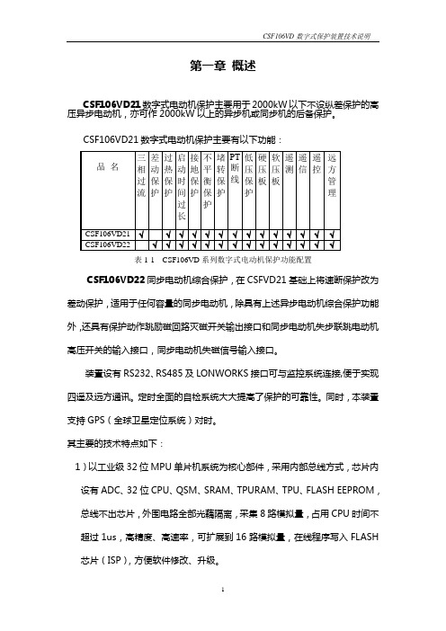
第一章概述CSF106VD21数字式电动机保护主要用于2000kW以下不设纵差保护的高压异步电动机,亦可作2000kW以上的异步机或同步机的后备保护。
表1-1 CSF106VD系列数字式电动机保护功能配置CSF106VD22同步电动机综合保护,在CSFVD21基础上将速断保护改为差动保护,适用于任何容量的同步电动机,除具有上述异步电动机综合保护功能外,还具有保护动作跳励磁回路灭磁开关输出接口和同步电动机失步联跳电动机高压开关的输入接口,同步电动机失磁信号输入接口。
装置设有RS232、RS485及LONWORKS接口可与监控系统连接,便于实现四遥及远方通讯。
定时全面的自检系统大大提高了保护的可靠性。
同时,本装置支持GPS(全球卫星定位系统)对时。
其主要的技术特点如下:1)以工业级32位MPU单片机系统为核心部件,采用内部总线方式,芯片内设有ADC、32位CPU、QSM、SRAM、TPURAM、TPU、FLASH EEPROM,总线不出芯片,外围电路全部光藕隔离,采集8路模拟量,占用CPU时间不超过1us,高精度、高速率,可扩展到16路模拟量,在线程序写入FLASH芯片(ISP),方便软件修改、升级。
2)128×64点大液晶全汉字显示,调试全部为汉字菜单结构,使用方便、直观、信息详尽丰富。
3)采用工业级芯片,表面贴工艺,体积小,抗震、抗干扰能力强、可靠性高。
4)前面板232串口带光电隔离,可在现场实现通讯,提供更加方便友好的调试操作环境。
5)结构上设计合理,全封闭机箱坚固、抗震、抗干扰能力强,机箱小巧,适合安装于保护屏、开关柜等处。
6)该保护共可录入4套保护定值,便于现场运行。
7)可扩展工业级CAN总线,LON总线网络,组网方便、经济、可靠、可与监控系统直接通讯。
8)自动记录故障数据,掉电不丢失,便于事故分析。
9)线路故障时,除提供光报信号外,保护自动弹出全中文故障报告,直观明了,便于维护。
- 1、下载文档前请自行甄别文档内容的完整性,平台不提供额外的编辑、内容补充、找答案等附加服务。
- 2、"仅部分预览"的文档,不可在线预览部分如存在完整性等问题,可反馈申请退款(可完整预览的文档不适用该条件!)。
- 3、如文档侵犯您的权益,请联系客服反馈,我们会尽快为您处理(人工客服工作时间:9:00-18:30)。
STV1601ASERIAL INTERFACE TRANSMISSION ENCODERNovember 199228293031323334351817161514131211102726252423222120193612345678937V E E D3X D4Y D4X D5Y D5X D6Y D6X D7Y D7XNCPCKTN1TRP FV GND PCY PCX RSE V CC V E E D 0YD 0XD 1YD 1XD 2YD 2XD 3Y L S TG N DS XS YG N DD 9XD 9YD 8XD 8Y1601A -01.E P SPIN CONNECTIONSPGA37(Ceramic Package)ORDER CODE :STV1601ATHIS IC CONT AINS ALL THE CIRCUITS NEEDED FOR CONVERSION FROM PARALLEL DATA,AND PARALLEL CLOCK,INTO SERIAL DATA.APPLICATIONS ARE STRAIGHTFORWARD AS ONLY A FEW EXTERNAL COMPONENTS ARE NEEDED.OTHER RELATED IC’s INCLUDE :.STV1602A,A SERIAL TRANSMISSION DE-CODER (WITH A BUILT-IN CABLE EQUAL-IZER AND PARALLEL-TO-SERIAL CONVERSION).STV1389AQ COAXIAL CABLE DRIVER STRUCTURE .Hybrid ICAPPLICATIONSSERIAL DATA TRANSMISSION ENCODER .100to 270Mb/s APPLICATIONS EXAMPLES.Serial data transmission of digital television signal 525-625lines.4:2:2component 270Mb/s (10-BIT).4*FSC PAL composite 177Mb/s (10-BIT).4*FSC NTSC composite 143Mb/s (10-BIT)FUNCTIONS.Parallel-to-serial conversion.Scrambler :Modulo -2division by G(x)=(x 9+x 4+1)(x +1).PLL for serial clock generation .PLL lock detection.Sync word required with the parallel data stream8bit10bit 1st word FFH 3FFH 2nd word 00H 000H 3rd word00H000HSync word conversion (8-bit timing reference signal is internally converted to 10-bit).CODE LIMITATIONThe word composing the Sync word listed above shall not appear during data words.This limitation includes 00and FF in 8-bit use and 000through 003and 3FC through 3FF in 10-bit use.DESCRIPTIONThe STV1601Ais a Hybrid IC encoderthat converts parallel data into serial data for a serial transmis-sion line.1/17PIN DESCRIPTIONPinNSymbol Equivalent circuitDescriptionI/OStandardMin.Typ.Max.Unit1LSTPLL lock detection.Is High while PLL locked.Ifunlocked,becomes irregular.At free running (TN1H)turns LowH LO-1.0-4.0V V36PCKClock output frequencydivided to 1/10VCO ed to check VCO free running frequencyH LO-0.8-1.6V V3SXDifferential Serial Output Input parallel data is converted to serial,then from scrambled NRZ to NRZI dataH LO-1.6-2.4V V4SY1601A -01.T B L1V CCGND2k Ω4k Ω2k ΩEEV 1601A -02.E P SGND EEV 36600Ω600Ω240Ω1601A -03.E P SGNDV CCV CC34EEV V R330Ω100Ω100Ω30Ω2k Ω2k Ω115Ω1601A -04.E P SSTV1601A2/17PIN DESCRIPTION(continued)PinN Symbol Equivalent circuit Description I/OStandardMin.Typ.Max.Unit29V CC Parallel data and clock input buffers power supply.Whenthis pin is connected to+5V, parallel data clock turns toTTL mode.When this pin is connected to GND,paralleldata clock turns to ECLmode.-6 7 8 9 10 11 12 13 14 15 16 17 18 19 20 21 22 23 24 25D9XD9YD8XD8YD7XD7YD6XD6YD5XD5YD4XD4YD3XD3YD2XD2YD1XD1YD0XD0YParallel input ports:LSB:D0X or YMSB:D9X or YSignal:DnXReturn:DnYFor ECL mode,V CC shalll be0VHLForTTL mode,VCC shall be+5VHL-1.02.0-1.60.8VVVV28RSEVCO range selectionH:high range140to270MHzL:low range100to145MHzHLI-0.4-4.0VV161A-2.TBL EEV29672kΩ1kΩV R3161A-5.EPSGNDEEV2870kΩ2kΩ10kΩ10kΩ161A-6.EPSSTV1601A3/17PIN DESCRIPTION(continued)PinN Symbol Equivalent circuit Description I/OStandardMin.Typ.Max.Unit30PCXParallel clock(PCX)and its return(PCY)For ECL mode,V CC=0HLFor TTL mode,V CC=+5VHL I-1.02.0-1.60.8VVVV31PCY2,5,32GND GND26V EE-5V power supplyI/O buffer PLL-5.2-5.0-4.8V27V EE-5V power supplyLogic part-5.2-5.0-4.8V33FV VCO free running frequencyadjustment:V EE level gives the lowestfrequency.To adjust,setTN1high.I-3.9V34TRP VCO input and phasecomparator output should beconnected to a parallel clockfrequency trap filter tominimize jitterO-3.2V35TN1Test mode:High:VCO free runningcondition(input disabled)Low:Normal mode(inputenabled)I-1.0-4.5VV161A-3.TBL EEV2kΩV R33031V CC2kΩ2kΩ161A-7.EPSGND3433E EV1kΩ1kΩ1kΩ1kΩ1kΩ10kΩ0.1µFV CC0.022µFV92µF220Ω161A-8.EPS1V CC GNDEEVV R320kΩ12kΩ4kΩ161A-9.EPSSTV1601A 4/17PLL LOCK DETECTOR VCOTIMING GENERATORNRZ ⊗NRZI000hex DETECTO RPHASE DETECT OR35303133342836PARALELL TO SERIAL CONVER TERX +X +1SCR AMBLER94134678910111213141516171819202122232425292726325237N.C.GNDGNDGNDV EEV EECCV PCY PCX TN1FV TRP RSE PCK LST SXSY D 9XD 9YD 8XD 8YD 7XD 7YD 6XD 6YD 5XD 5YD 4XD 4YD 3XD 3YD 2XD 2YD 1XD 1YD 0XD 0YParallel ClockS e r i a l C l o c kP a r a l l e l L o a d10-BIT X 3WORD SHIFT REGISTER1601A -10.E P SBLOCK DIAGRAMABSOLUTE MAXIMUM RATINGSSymbol ParameterValue Unit V EE Supply Voltage -6V V CC Supply Voltage +6V V IN Input Voltage V EE to V CCV I OUT Output Current-30mA T oper Operating Temperature 0to 65o C T stg Storage Temperature-50to 125o C P DAllowable Power Dissipation2.0W1601A -04.T B LRECOMMENDED OPERATING CONDITIONSSymbol ParameterValue Unit V EE Supply Voltage -4.8to -5.2V V CC Supply Voltage *4.8to5.2V T operOperating Temperature 0to 65o C*For TTL input.Voltages are given with respect to GND1601A -05.T B L ELECTRICAL CHARACTERISTICS (V EE =-5V,V CC =GND/+5V,T A =25o C unless otherwise speciied)Symbol ParameterTest ConditionsTest Circuit Min.Typ.Max.Unit DC CHARACTERISTICSI EE Supply Current 1Figure 2140mA I CCSupply Current 27mA 1601A -06.T B LSTV1601A5/17ELECTRICAL CHARACTERISTICS (V EE =-5V,V CC =GND/+5V,T A =25o C unless otherwise speciied)Symbol ParameterTest Conditions Test Circuit Min.Typ.Max.Unit DC CHARACTERISTICSV IH Input VoltageV CC =GNDPCX,PCY,DnX,DnY -1.0V V IL -1.6V V IH V CC =+5VPCX,PCY,DnX,DnY 2.0V V IL 0.8V I IH Input CurrentPCX,PCY,DnX,DnY Figure 35µA I IL -1+1µA V IH Input VoltageRSEFigure 7-0.4V V IL -4.0V V IH TN1Figure 6-1V V IL -4.5V V OH Output VoltagePCKR P =1k Ω-0.8V V OL -1.6V V OH LSTI OH =-10µA,I OL =+10µA Figure 5-1.0V V OL -4.0V V OH SX,SY R P =220Ω-1.6V V OL -2.4V AC CHARACTERISTICSf MAX1VCO Max.Oscillation Frequency 1RSE =”H”Figure 430.0MHz f MIN1VCO Min.Oscillation Frequency 114.0MHz f MAX2VCO Max.Oscillation Frequency 2RSE =”L”15.0MHz f MIN2VCOMin.Oscillation Frequency 210.0MHz f HP1PLL Pull in Rangef signal =270MHz RSE =”H”Figure 127.7MHz f LP125.5MHz f HP2f signal =177MHz RSE =”H”18.8MHz f LP216.5MHz f HP3f signal =143MHz RSE =”H”15.0MHz f LP313.0MHz f OP1PLL Generator Frequency RSE =”H”14.027.0MHz f OP2RSE =”L”10.014.5MHztjitJitterf signal =270MHz RSE =”H”Figure 8±0.25nsecTested through PCK :1/10of serial clock.1601A -07.T B LSWITCHING CHARACTERISTICS (V EE =-5V,V CC =GND/+5V,T A =25o C unless otherwise speciied)SymbolParameterTest Conditions Test Circuit Min.Typ.Max.Unit t r Rise Time PCKR P =1k ΩFigure 100.8nsec t f Fall Time 1.4nsec t r Rise Time SX,SY R P =220Ω0.7nsec t fFall Time0.7nsec1601A -08.T B L TIMING RELATION OF INPUT CLOCK AND DATASymbol ParameterTest Conditions Test CircuitMin.Typ.Max.Unit t w Pulse Width PCX,PCY Figure11-5+t c /2t c /2+5+t c /2nsec t dDelay TimePCX -Dn-5+5nsec1601A -09.T B LSTV1601A6/17H P 8180A S I G N A L G E N E R A T O R3031678910111213141516171819202122232425D 0YD 0XD 1YD 1XD 2Y D 2XD 3YD 3XD 4Y D 4X D 5YD 5XD 6YD 6XD 7Y D 7XD 8YD 8XD 9YD 9XP C XP C Y2532292726G N D V C CV E E0.110/16V0.110/16V 373328N .C .35-5V-5V-5VS W 1S W 2A B10µF /10V22k ΩA BH I G H R A N G EL O W R A N G E V C O R A N G E S E L E C TO N :A F F R E Q U E N C Y A D J U S T150p F0.22µH34T R P T N 1-5V 36P C K 1k ΩF R E Q U E N C Y M O N I T O R 1L S T 34220Ω220Ω-5V 0.1220ΩS XS YD .U .T .S T V 1601A0.1V C O F R E Q U E N C Y A D J U S T10k ΩV R 10.1220Ω-5V220Ω0.10.10.1-5V 0.10.1220Ω150Ω150Ω75Ω75Ω12S E R I A LO U TV R V C CE E V -5VI N P U T L E V E LT T L E C L+1.4V -1.3V +5V G N DS T V 1389A QP L L L O C K D E T E C T O R3334D I XD I Y220Ω0.1-5V220Ω220Ω252628A I YA I XQ F S73Ω41p F41p FM O N 31100ΩA B S E R I A L I NC X29A D S32S W 2-5V10k ΩS YS X 432G N D V E E0.10.110/16V2427302387-5VA B I N P U T S E L E C TC A B L E I N P U TD I G I T A L I N P U TS T V 1602A-5V V C O F R E Q U E N C Y A D J U S T10k ΩF V36V R 2E S O E S IR S E 22137D P R35-5V0.120S Y N E V R P C K D 0D 121191817-5V0.11k Ωx 4T R S D E T E C T O R S I G N A L F R E Q E N C Y M O N I T O R D 2D 3D 4D 5D 6D 7D 8D 91615141312111091k Ωx 822k ΩT N 1100k ΩQ S W65S W 310µF-5V0.1L E D330ΩO N :A F F R E Q U E N C Y A D J U S TH P 8182AS I G N A L A N A L Y Z E RF V R S E10µF1601A -11.E P SFigure 1:Test Circuit Diagram ExampleSTV1601A7/17253229A A 27263034352833PCX SXSYFV RSE TN1GNDV CCEEV V R110k Ω22k Ω10µF-5V-5V-5V SW1SW1ONPOSITION 0.1µF220Ω220Ω1k Ω10/16V10/16V0.10.1EEI CCI EE V -5VCC V +5V STV1601A1601A -12.E P SFigure 225322927263034352833PCX SXSY FV RSE TN1GNDV CCEEV V R110k Ω22k Ω10µF-5V-5V-5V SW1POSITION 0.1µF220Ω220Ω1k Ω10/16V0.1STV1601A-5V3031PCXPCY1112V 2V 1SW2ONSW2-5VABA1A2I ILI IH I IL I IHV 1V 2SW1ANY -0.8V-1.6V-1.6V -0.8V1601A -13.E P SFigure 4STV1601A8/1725322927263034352833PCX SX SYFV RSE TN1GNDV CCEE V V R110k Ω22k Ω10µF-5V-5V-5V SW1POSITION0.1µF220Ω220Ω1k Ω10/16V 0.1STV1601A-5VSW2ON SW2-5VABFREQUENCY MONITOR A ON B HIGH LOWSW1VCO RANGE 1601A -14.E P SFigure 42532292726352833FV RSE TN1GNDV CCEEV V R110k Ω22k Ω10µF-5V-5VSW1POSITION 10/16V 0.1STV1601A-5V3031PCX PCYV 2V 1SW2SW2-5VABV 1V 2V OH V OLV SW1OFF1LST VANY -0.8V -1.6V-1.6V -0.8V1601A -15.E P SFigure 5STV1601A9/1725322927262833FVRSE GNDV CCEEV V R110k Ω-5V10/16V 0.1STV1601A-5V3031PCX PCYV 11LSTVTN131-0.8V-1.6V1601A -16.E P SFigure 6253229272630343533PCX SX SYFV TN1GNDV CCEE V V R110k Ω22k Ω10µF-5V-5V-5V 0.1µF220Ω220Ω1k Ω10/16V 0.1STV1601A-5VSW2FREQUENCY MONITOR 28RSEV 11601A -17.E P SFigure 7253229272630343533PCX SX SYFV TN1GNDV CCEE V V R110k Ω22k Ω10µF-5V-5V-5V0.1µF 1k Ω10/16V 0.1STV1601A-5VSW2FREQUENCY MONITOR 28RSE -5V220Ω220Ω220Ω0.1-5V0.1µF150Ω150Ω0.10.175Ω75Ω12STV1389AQParallel clock dataTRIGGERSIGNALSERIAL OUTSIGNAL 270Mb/sjitter =1/2t1601A -18.E P SFigure 8STV1601A10/1780%20%t t r f1601A -19.E P SFigure 9:t r ,t f Definition50%t ct d t wc t /2c t /21601A -20.E P SFigure 10:t d ,t W DefinitionDESCRIPTIONSTV1601A internally generates a 10times clock frequencylocked to the parallel input clock thanks to a built-in PLLand converts input parallel data into serial data.To ease clock extraction at the receiving end,serial data is scrambled.T o minimize polarityeffect,serial data is then converted to NRZI and output in differ-ential mode.A PLL lock detection circuit only enables the serial output when locked.1.Phase relation between input parallel clock and dataThe phase relation between the parallel clock and the data is shown in Figure 11.Both clock and data are differential inputsParallel clock and data are such that the rising edge of PCX should be at the middle of the data.A clock having the same phase as PCX is internally gener-ated in order to latch the data.2.TTL input operationParallel clock and data can be either TTL or ECL inputs.To use as TTL inputs VCC (Pin 29)shall be connected to +5V.A fixed bias of +1.4V shall be applied to PCY and DnY (n =0to 9).TTL signals and their parallel clock will be provided through 1kW resistors to each ”X”input.These 1kW resis-tors are effective to minimize the influence of the TTL input signals to the jitter characteristics of the serial output signal.For 8-bit data,unused LSB(s)must be fixed Low.Fixed bias value can be higher,for example,2.5V in case of CMOS inputs.PCX (Input)DATA (Input)PCX (Output)1601A -21.E P SFigure 11:Phase Relation between Clock and Data293031572625Parallel Clock Parallel Data+5V+1.4V for TTL +2.5V for CMOSD0Y D0X D9Y D9X PCY PCX V CC TTL Parallel SignalSTV1601A1k Ω1k Ω1k Ω1601A -22.E P SFigure 12:TTL Input Operation11/173.PLL blockPARALLEL CLOCK INPUT CONTROLPLL,PLL lock detection and the various blocks of the serial output control are shown in Figure 13.When TN1is connected to GND (set High),the parallel clock input is disabled.The VCO turns to free running conditions and its frequency can be adjusted through FV.This frequency decreases when the resistor value between FV and V EE is reduced.Oscillation fre-quency monotoring is performed through PCK which delivers a frequency divided by ten.When PLL is locked,PLL and PCX input signal phases are nearly matched.The RC network con-nected to TN1,temporarily,disables the parallel clock in order to avoid mislocking problems.VCO oscillation frequency range selection is avail-able through RSE ;High :from 140to 270MHz ;Low :from 100to 145MHz.TRP (Pin 34)is the phase comparator output.To minimize jitter,a trap circuit,consisting in a serial tuned circuit at parallel clock frequency can be used.PLL LOCK DETECTIONThe LST signal is generated by latching the incom-ing parallel clock by the internal one (which is 1/10of the VCO frequency).LST is used as a PLL lock detection signal and also controls the serial output.If the parallel clock input is disabled (by means of TN1),LST turns Low and the serial output is dis-abled as described in the previous section (SX (Pin 3)=High,SY (Pin 4)=Low).If the serial output has to be disabled while no parallel clock input is provided,PCX must be set Low and PCY must be set High.4.Sync wordTo convert serial data back to parallel,insertion of some timing reference data indicating the parallel data word boundary in the serial data is needed.This,called TRS (Timing Reference Signal)in the digital interface format,consists of the three con-secutive words 3FFH,000H,000H.Conversion to 10-bit TRS from 8-bit (TRS)8-bit parallel data8-bit parallel data can be converted into 10-bit data by using the 8th bit as the MSB and by setting the 2LSBs at logical states as shown in Figure 14.LST SXSYSerial ClockPCY PCXTN1FV TRPRSEPCKPHASE COMPARATORVCO 1/10DIVIDERNRZ To NRZI CONVERSIONSCRAMBLERQDQ D”0”1601A -23.E P SFigure 13:PLL and Serial Output Control Block12/1725D0Y D0X V STV1601A242322D1X D1Y EE6218-bit Parallel Data10k Ω1601A -24.E P SFigure 14:8-bit Parallel Input Data (ECL level)The conversion algorithm detects 2successive 000H words and sets the two LSBs of the previous word,which is supposed to be FF,according to the standard.001001001001001001001001000Input DataFixed Data00100100100100100100100100011MSBLSBInput Order Parallel Data after ConversionInput Parallel Data 01601A -25.E P SFigure 10:Conversion from 8-bit TRS to10-bit TRSConversion in the case of more than three succes-sive ”000H”words.If more than 3consecutive words of 000in D1standard,or 4consecutive words of 000in D2standard occur at the parallel input (illegal accord-ing to the standard),thus no proper operation is possible.5.Scrambling and NRZ to NRZI conversion Figures 16and 17show the scrambling circuit,the scrambling polynomial is as follows :x 9+x 4+1.D1D2D3D4D5D6D7D8D91601A -26.E P SFigure 16:(x 9+x 4+1)Basic Scrambling CircuitD1D2D3D4D5D6D7D8D91601A -27.E P SFigure 17:(x 9+x 4+1)Basic Scrambling CircuitTo eliminate signal polarity of scrambled data,con-version from NRZ to NRZI is performed (Figures18and 19).Therefore,the polarity for output distribution or receiving is not needed.This allows easy system design.The NRZ to NRZI polynominal is x +1.VCO temperature compensation and oscillation frequency adjustmentVCO oscillation frequency depends on the tem-perature as shown in Figures 22and 23”Repre-sentative characteristics examples”.Within the normal range of operation,frequency increases with temperature.FV voltage remains almost con-stant regardless of temperature.Figure 20shows an example of a temperature compensation circuit using a diode (transistor with C-B diode short-cir-cuited)and a resistor connected between FV and V EE .Examplesof representativecharacteristics for various temperatures are shown in Figures 22and 23concerning oscillation frequency and PLL pull-in range (signal frequency 270,177and 143MHz).VCO free running frequency adjustmentVCO free running frequency adjustment is per-formed at room temperature.If TN1is set High,VCO free runs.Wait for 5to 10minutes after turning power supply ON (warm up time).While monitoring PCK output (Pin 36)adjust the signal frequency (within ±1%)with the variable resistor connected between FV and V EE .13/17Jitter trapSince the internally generated serial clock is locked to the incoming parallel clock,there exists periodic jitter components which are generated from the phase comparison process of the PLL.A serial resonant circuit (trap)connected between TRP (Pin 34)and V EE tuned at the parallel clock frequency reduces effectively the fundamental component of the jitter well below the specification (±0.25ns).Recommended values of C1and L1are given in the following table.RECOMMENDED VALUES OF THE TRAP CIRCUIT COMPONENTSTANDARDD1D2PAL NTSC C1(pF)150240300L1(µH)0.20.30.4An important remark in a practical implementation is that TRP node is an input of a very sensitive voltage-frequency converter (VCO)which can be easily disturbed by any pick-up noise.Hence,the trap circuit should be carefully located and be kept as short as possible from the Pin 34in order to avoid noise problems.V EESTV1601A10k ΩTN1353336FV Small signal transistorFrequency monitor 10µF22k Ω1k ΩPCK TRP 34C1L11601A -30.E P SFigure 20:VCO Temperature Compensation and Free Running AdjustmentTime scaleNRZI signalNRZ signalNRZI signalNRZI inverted signalNRZ to NRZI conversionNRZ to NRZI conversion1601A -29.E P SFigure 19:Relation between NRZ and NRZI Signals14/173736353433323130N .C .P C K T N 1T R P F V G N D P C Y P C X -5V -5V22k Ω1k Ω10µF /16VC 1L 1Q 110k Ω4.7k Ω2.2k Ω51Ω51Ω0.10.1-5V2928R S E V C C V E EV E E 2627H I G H L O WD 0Y D 0XD 1Y D 1X D 2YD 2X D 3Y 25242322212019181017161514131211D 7XD 7YD 6XD 6YD 5XD 5Y D 4XD 4YD 3X123456789D 8Y D 8X D 9YD 9X G N DS Y S X G N D L S T P a r a ll e l D a t a I N (E C L B a l a n c e d P a i r )C 1L 1D 2P A L U n i t 1512100.23000.4D 10.3R e c o m m e n d e d v a l u e s-5V 0.1µF220Ω220Ω220Ω0.1µF0.1µF-5V-5V 150Ω150Ω220Ω220Ω0.1µF 0.1µF1k Ω68Ω68ΩP a r a l l e l C l o c k I nT e s t J u m p e rP a r a l l e l C l o c k T e s t P o n i t (R e t u r n )(R a t e s e l e c t )-5V ((115m A t y p i c a l )N T S C µHF o r s i g n a l P r o c e s s i gF o r c o a x i a l c a b l e p r o c e s s i n gn F S T V 1601A(E N C O D E R M O D U L E )S T V 1389A QD 2N T S CD 1,D 2P A L10k Ω1601A -31.E P SFigure 21:Application Circuit Example15/170.800.90 1.00 1.10 1.20 1.30300260220180140FV pin Voltage (V)V C O o s c i l l a t i o n f r e q u e n c y (M H z )RSE:”H”85°C65°C45°C 25°C 5°C -15°C 1601A -32.E P SFigure 22:VCO Oscillation Frequency versusFV Pin VoltageEXAMPLE OF REPRESENTATIVE CHARACTERISTICS 0.901.00 1.101.20 1.30FV pin Voltage (V)V C O o s c i l l a t i o n f r e q u e n c y (M H z )10011012013014015085°C65°C45°C25°C5°C-15°CRSE :”L”1601A -33.E P SFigure 23:VCO Oscillation Frequency versusFV Pin Voltage-15525456585Ambient temperature (°C)3029282726252423F r e q u e n c y (M H z )High pull in Free runLow pull in1601A -34.E P SFigure 24:Pull in Range and Free Run Fre-quency (270Mb/s)-15525456585Ambient temperature (°C)1817161514131211F r e q u e n c y (M H z )High pull inFree runLow pull in1601A -36.E P SFigure 26:Pull in Range and Free Run Fre-quency (143Mb/s)-15525456585Ambient temperature (°C)2120191817161514F r e q u e n c y (M H z )Free runHigh pull inLow pull in1601A -35.E P SFigure 25:Pull in Range and Free Run Fre-quency (177Mb/s)16/17Bottom View25.40.50.460.051.20.125.40.53.81.150.154.2Seating plane0.22.54x 9=22.860.25Pin 28Pin 19Pin 36Pin 10Pin 1Pin 372.542.542.032max.2.54x 9=22.860.25Dimensions in mmP M -P G A 37.E P SPACKAGE MECHANICAL DATA 37PINS -CERAMIC PGAInformation furnished is believed to be accurate and reliable.However,SGS-THOMSON Microelectronics assumes no responsibility for the consequences of use of such information nor for any infringement of patents or other rights of third parties which may result from its use.No licence is granted by implication or otherwise under any patent or patent rights of SGS-THOMSON Microelectronics.Specifications mentioned in this publication are subject to change without notice.This publication supersedes and replaces all information previously supplied.SGS-THOMSON Microelectronics products are not authorized for use as critical components in life support devices or systems without express written approval of SGS-THOMSON Microelectronics.©1994SGS-THOMSON Microelectronics -All Rights Reserve dPurchase of I 2C Components of SGS-THOMSON Microelectronics,conveys a license under the Philips I 2C Patent.Rights to use these components in a I 2C system,is granted provided that the system conforms tothe I 2C Standard Specifications as defined by Philips.SGS-THOMSON Microelectronics GROUP OF COMPANIESAustralia -Brazil -China -France -Germany -Hong Kong -Italy -Japan -Korea -Malaysia -Malta -Morocco The Netherlands -Singapore -Spain -Sweden -Switzerland -Taiwan -Thailand -United Kingdom -U.S.A.17/17。