AAT7126IAS-T1中文资料
TEA1716中文资料免费版
TEA1716T中文资料免费版1. General descriptionTEA1716T集成了功率因数校正器(PFC)控制器和半桥谐振变换器的控制器(HBC)multi-chip IC。
它提供了离散MOSFET的驱动功能在一个上升变换器和两个离散功率场效应管谐振半桥配置。
高效PFC操作是通过实现准谐振软开关技术(QR)操作功能在高功率水平与QR操作谷跳跃在低功率水平。
过电流保护(OCP)、过电压保护装置(OVP)和退磁传感在所有条件下确保安全运行。
HBC模块是一个高压零开关LLC谐振变换器的控制器。
它包含一个高压电平转变电路和保护电路包括OCP,开环保护,电容模式保护和通用门锁保护输入。
高压芯片制作用的是专用高压Bipolar-CMOS-DMOS功率逻辑处理能够有效的从电源电压直接启动。
低压绝缘硅片(SOI)芯片用于准确、高速的保护功能和控制。
TEA1716T控制PFC电路和谐振转换器是非常灵活的。
它可以用于广泛的应用在一个宽的电源电压范围。
PFC和HBC控制器结合在一个单一的电源控制IC 使TEA1716T理想在液晶和等离子电视。
使用TEA1716T提供高效、可靠的电力供应从90 W到500 W可以轻松地使用TEA1716T设计,用最少的外部组件。
TEA1716T的集成突发模态和电源管理功能使共振的应用程序满足能源使用产品指令(EuP)很多6(< 0.5 W在待机模式)。
2.1 General features集成PFC和HBC控制器通用电源运行从70V-276V (AC)高水平的集成导致较低的外部组件数量和成本效益的设计集成突发模式感应符合能源使用产品指令(EuP)6使能输入只允许使能PFC或者PFC和HBC控制器芯片上的高压启动源独立运行或从DC源供应2.2 PFC controller features及时控制边界模式操作谷底和零电压开关以致最小损耗频率限制来减少开关损耗精确的增压调节用软启动和软停止的突发模式开关2.3 HBC controller features集成高压电平位移器可调节最大和最小频率半桥开关频率最大可达500KHz合适的非重叠时间突发模式开关2.4 Protection features安全系统故障条件下重启模式通用门锁保护输入对输出过电压保护或外部温度保护保护定时器超时并重启过温保护对两个控制器软启动欠电压保护给电源(断电),增压,IC供应和输出电压对两个控制器进行过流保护和调节对增高电压精确的过压保护对HBC控制器容性模式保护3. ApplicationsLCD电视等离子电视笔记本适配器台式机6.2 Pin descriptionCOMPPFC 1 PFC控制器频率补偿,外部链接到过滤器SNSMAINS 2 电源电压输入感应;外部连接分压电阻电源电压SNSAUXPFC 3 PFC消磁时间感应输入;外部连接到PFC的辅助绕组SNSCURPFC 4 PFC控制器为瞬时电流和软启动检测输入;外部连接到电流检测电阻和软启动过滤器SNSOUT 5 检测输入监测HBC输出电压;外部连接到辅助绕组SUPIC 6 SUPIC低压输入和输出的内部高压启动源;外部连接到辅助绕组HBC 或外部直流供电GATEPFC 7 PFC MOSFET 门极驱动输出PGND 8 电源地,HBC和PFC参考地SUPREG 9 管理SUPREG IC供应;内部调节器输出,输入驱动;外部连接到SUPREG缓冲电容器GATELS 10 HBC 低边MOSFET 门驱动输出n.c. 11 不连接SUPHV 12 内部高压启动源供应源高压输入;外部连接来提高电压GATEHS 13 HBC 高边MOSFET门驱动输出SUPHS 14 高端的驱动提供输入;外部连接到自举电容(CSUPHS)HB 15 参考高端驱动和半桥斜坡输入检测;外部连接到半桥节点HB的HBC mosfet之间(参见图17)n.c. 16 不连接SNSCURHBC 17 瞬时HBC检测输入;外部连接到谐振电流检测电阻SGND 18 信号地和IC参考地CFMIN 19 HBC最低频率设置;外部连接的电容器SNSBURST 20 突然停止激活检测输入;外部连接分压电阻SNSFB电压SNSFB 21 输出电压调节反馈检测输入;外部连接到光耦合器和上拉电阻SSHBC/EN 22 HBC软启动t时间和IC使能输入;使能PFC或PFC只或PFC和HBC控制器;外部连接到s软启动电容器,使下拉的信号RCPROT 23 保护定时器设置超时并重启;外部连接的电阻器和电容器SNSBOOST 24 检测输入增加电压调整;外部连接分压电阻提高电压7. Functional descriptionTEA1716T可以组合的功能如下:电源模块:IC供应管理。
IAD012YJJG资料

DescriptionFeatures•RoHS lead-solder-exemption compliant •Industry-standard package •Industry-standard footprint •Fixed-frequency design •85 °C case operation •Optional trim and enable •Wide-range input •1500 V isolation•Short-circuit protectionIAD dual-output dc-dc converters provide up to 12 watts of output power in an industry-standard package and footprint. With a maximum case temperature of 85 °C, the IAD is well suited for the most demanding applications. The IAD features 1500 VDC isolation, short circuit, and overtemperature protection, as well as six-sided shielding. The IAD is available with optional enable and voltage trim pins. Please see the IAS series for single-output applications.GeneralTurn-On Time 300 ms Remote Shutdown Positive LogicSwitching Frequency 400 kHz IsolationInput - Output1500 VDC Output - Case (for 48 V in )500 VDC Input - Case (for 24 V in )1050 VDC Temperature Coefficient ±0.03%/°C Case Temperature Operating Range -40 To +85 °C Storage Range-40 To +110 °CHumidity Max., Non-Condensing 95%Vibration, 3 Axes, 5 Min Each5 g, 10 - 55 Hz MTBF †(Bellcore TR-NWT-000332) 1.8 X 10⁶hrs SafetyUL, cUL, VDEWeight (Approx.)1.2 ozTechnical SpecificationsVoltage Range 24 VDC Nominal 18 - 36 VDC 48 VDC Nominal 34 - 75 VDCReflected Ripple25 mA Input Reverse Voltage ProtectionShunt DiodeInputOutputSetpoint Accuracy±1%Auxillary Setpoint Accuracy5 %Line Regulation V in Min. - V in Max., I out Rated 0.5% V out Load Regulation I out Min. - I out Max., V in Nom. 1.0% V out Minimum Output Current10 % I out RatedDynamic Regulation, Loadstep 25% I out Pk Deviation 4% V out Settling Time 500 μs Voltage Trim Range±10%Short Circuit / Overcurrent Protection Hiccup Power Limit Threshold Range110 - 150%Notes†MTBF predictions may vary slightly from model to model.†† Industrial temp range availableSpecifications typically at 25 °C, normal line, and full load, unless otherwise stated.Soldering Conditions: I/O pins, 260 °C, ten seconds; fully compatible with commercial wave-soldering equipment.Safety: Agency approvals may vary from model to model. Please consult factory for specific model information.Units are water-washable and fully compatible with commercial spray or immersion post wave-solder washing equipment.NOTES:* Maximum input current at minimum input voltage, maximum rated output power.** At nominal V in , rated output.Model numbers highlighted in yellow or shaded are not recommended for new designs.Mechanical DrawingThermal Impedance Natural Convection 15.4 °C/W 100 LFM 12.2 °C/W 200 LFM 9.3 °C/W 300 LFM 7.4 °C/W 400 LFM6.4 °C/WNote:Thermal impedance data is dependent on many environmental factors. The exact thermal performance should be validated for specific application.Pin Function 1+V in 2-V in 3Optional Shutdown 4+V out 5Common 6-V outTolerancesInches: (Millimeters).XX ± 0.020 .X ± 0.5.XXX ± 0.010 .XX ± 0.25 Pin:± 0.002 ± 0.05Case:+ 0.04, - 0.00 + 1.0, - 0.0(Tolerances as listed unless otherwise specified.)Model SelectionNUCLEAR AND MEDICAL APPLICATIONS - Power-One products are not designed, intended for use in, or authorized for use as critical components in life support systems, equipment used in hazardous environments, or nuclear control systems without the express written consent of the respective divisional president of Power-One, Inc.TECHNICAL REVISIONS - The appearance of products, including safety agency certifications pictured on labels, may change depending on the date manufactured. Specifications are subject to change without notice.。
fp7126规格书

fp7126规格书FP7126规格书FP7126规格书是一份详细描述产品规格和性能的文件,旨在帮助用户全面了解FP7126的特点和功能。
本文将从多个角度对FP7126进行介绍,包括产品概述、外观设计、性能指标、适用范围以及使用注意事项等内容。
一、产品概述FP7126是一款高性能的电子产品,采用先进的技术和优质的材料制造而成。
该产品具有出色的功能和稳定的性能,可广泛应用于各个领域。
FP7126的设计理念是为用户提供便捷、高效和可靠的使用体验。
二、外观设计FP7126外观简约大方,采用现代化的设计风格。
产品外壳采用高强度材料制成,具有良好的耐磨、抗冲击和防水性能。
同时,FP7126还配备了人性化的按键和显示屏,操作简单直观,用户可以轻松掌握各项功能。
三、性能指标1. 处理器:FP7126采用先进的处理器,具有高速运算能力和低能耗特性,能够满足用户对于高性能的需求。
2. 存储容量:FP7126配备大容量的存储空间,可支持大量数据的存储和快速访问。
3. 电池续航:FP7126的电池续航能力优秀,能够满足用户长时间使用的需求。
4. 通信功能:FP7126支持多种通信方式,包括蓝牙、WIFI等,用户可以方便地进行数据传输和网络连接。
5. 屏幕显示:FP7126的屏幕采用高分辨率显示技术,色彩鲜艳、清晰度高,用户可以获得更好的视觉体验。
四、适用范围FP7126适用于各个行业和领域,包括但不限于金融、通信、医疗、物流等。
无论是商务办公、数据处理还是移动办公,FP7126都能够提供卓越的性能和可靠的支持。
五、使用注意事项1. 在使用FP7126之前,请仔细阅读产品说明书,了解产品的功能和使用方法。
2. 在使用过程中,请避免将FP7126暴露在极端温度、潮湿或尘埃较多的环境中,以免影响产品性能和寿命。
3. 请勿将FP7126与尖锐物体或强磁场接触,以免刮伤或损坏产品。
4. 使用过程中请注意保护产品的屏幕,避免受到撞击或挤压。
31262中文资料

31262 Product Details
Ring and Spade Tongue Terminals
Always EU Rock Links
) Check Pricing & Availability Search for Tooling Product Feature Selector Contact Us About This Product
Industry Standards: ? Government/Industry Qualification = No ? RoHS/ELV Compliance = RoHS compliant, ELV compliant ? Lead Free Solder Processes = Not relevant for lead free process ? RoHS/ELV Compliance History = Always was RoHS compliant Packaging Related Features: ? Packaging Method = Box ? Packaging Quantity = 1,000 Other: ? Brand = AMP
( Statement of Compliance
31262
Active
Product Highlights: ? Terminal Shape = Ring Tongue ? Receptacle Style = Straight ? Body Style = Budget ? Barrel Type = Closed Barrel ? Wire/Cable Type = Regular Wire View all Features | Find Similar Products
芯片TPS7A1601资料
225
400
mA
IGND接地电流
3 V≤VIN≤60 V, IOUT = 10μA
5
15
μA
IOUT = 100mA
5
μA
ISHDN关闭电源电流
VEN = 0.4 V
μA
I FB反馈电流
0.59
5.0
μA
IEN使能电流
3 V≤VIN≤12 V, VIN = VEN
-1
0.0
1
μA
VEN_HI高使能电压
–0.3
5.5
V
DELAY引脚到GND引脚
–0.3
5.5
V
电流
最高输出
内部限制
温度
操作虚拟结点TJ,相对最大范围
-40
150
°C
储存温度Tstg
-65
150
°C
静电放电评级
人体模型(HBM)AEC-Q100分类等级H2
2
kV
带电器件模型(CDM)AEC-Q100分类等级C3B
750
V
二、电气特性
At TA= –40°Cto125°C, VIN = VOUT(NOM) + 0.5 V or VIN = 3 V (哪个更大), VEN = VIN, IOUT = 10μA, CIN = 1μF, COUT = 2.2μF,FB连接OUT
1.2
V
VEN_LO低使能电压
0.3
V
VIT
OUT引脚漂浮VFB增加,VIN≥VIN_MIN
85%
95%
VOUT
OUT引脚漂浮VFB减小,VIN≥VIN_MIN
83%
93%
VOUT
PT4126A中文资料

—
500
15
23
1.3 1.6 4.0 5.0 75.0 ±1.5 ±50 — ±1.0 ±33 ±1.0 ±33 — — — — — — — — — — — — — 700 900 —
7.0 (2) +0.8 – 50 — 200 — — — +85 (3) +125
0.1A/µs, load step 50% to 100% Iomax
Vo over/undershoot
Vo ≥ 5.0Vge
Vo ≥ 12.0V Vo ≤ 5.2V
Referenced to –Vin (pin 2)
pins 1 & 2 connected
Mechanical Shock
Mechanical Vibration
Weight Flammability
Io
Vin Vo tol
Regtemp Regline
Regload
∆Votot
η
Vr
ttr ∆Vtr Isc ƒs UVLO VIH VIL IIL Iin standby Cin Cout
Ta Ts MTBF — — — —
Over Vin range
Vo = 15V Vo = 12V Vo =5.0V Vo ≤ 3.3V
Over Io Range
Vo ≥5.0V
Vo ≤3.3V
–40° ≤Ta ≤ +85°C
Over Vin range
Vo ≥5.0V
Vo ≤3.3V
Over Io range
Description
The PT4120 power modules are a series of isolated DC/DC converters housed a lowprofile package. Rated for 20 watts or 5A, the series includes standard output voltages ranging from as low as 1.5VDC to 15VDC. The output may be adjusted ±10% of nominal. These converters are ideal for Telecom, Industrial, Computer, and other distributed power applications that require input-tooutput isolation.
阿特瓦尔71系列变频器产品数据表说明书
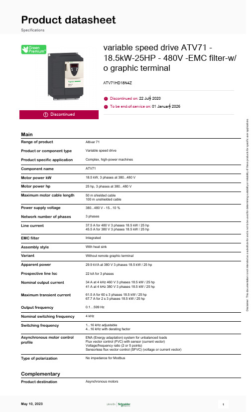
Product datasheetSpecificationsDiscontinuedvariable speed drive ATV71 -18.5kW-25HP - 480V -EMC filter-w/o graphic terminalATV71HD18N4ZDiscontinued on:22 July 2020To be end-of-service on:01 January 2026MainRange of productAltivar 71Product or component type Variable speed driveProduct specific application Complex, high-power machines Component name ATV71Motor power kW 18.5 kW, 3 phases at 380...480 V Motor power hp25 hp, 3 phases at 380...480 V Maximum motor cable length 50 m shielded cable 100 m unshielded cable Power supply voltage 380...480 V - 15...10 %Network number of phases 3 phasesLine current 37.5 A for 480 V 3 phases 18.5 kW / 25 hp 45.5 A for 380 V 3 phases 18.5 kW / 25 hp EMC filter Integrated Assembly style With heat sinkVariantWithout remote graphic terminalApparent power 29.9 kVA at 380 V 3 phases 18.5 kW / 25 hp Prospective line Isc 22 kA for 3 phasesNominal output current 34 A at 4 kHz 460 V 3 phases 18.5 kW / 25 hp 41 A at 4 kHz 380 V 3 phases 18.5 kW / 25 hp Maximum transient current 61.5 A for 60 s 3 phases 18.5 kW / 25 hp 67.7 A for 2 s 3 phases 18.5 kW / 25 hp Output frequency0.1…599 Hz Nominal switching frequency 4 kHzSwitching frequency 1...16 kHz adjustable4...16 kHz with derating factorAsynchronous motor control profileENA (Energy adaptation) system for unbalanced loads Flux vector control (FVC) with sensor (current vector)Voltage/frequency ratio (2 or 5 points)Sensorless flux vector control (SFVC) (voltage or current vector)Type of polarizationNo impedance for ModbusComplementaryProduct destination Asynchronous motorsD i s c l a i m e r : T h i s d o c u m e n t a t i o n i s n o t i n t e n d e d a s a s u b s t i t u t e f o r a n d i s n o t t o b e u s e d f o r d e t e r m i n i n g s u i t a b i l i t y o r r e l i a b i l i t y o f t h e s e p r o d u c t s f o r s p e c i f i c u s e r a p p l i c a t i o n sSynchronous motorsPower supply voltage limits323…528 VPower supply frequency50...60 Hz - 5...5 %Power supply frequency limits47.5...63 HzSpeed range1…100 for asynchronous motor in open-loop mode, without speed feedback1…1000 for asynchronous motor in closed-loop mode with encoder feedback1…50 for synchronous motor in open-loop mode, without speed feedbackSpeed accuracy+/- 0.01 % of nominal speed in closed-loop mode with encoder feedback 0.2 Tn to Tn+/- 10 % of nominal slip without speed feedback 0.2 Tn to TnTorque accuracy+/- 15 % in open-loop mode, without speed feedback+/- 5 % in closed-loop mode with encoder feedbackTransient overtorque170 % of nominal motor torque +/- 10 % for 60 s every 10 minutes220 % of nominal motor torque +/- 10 % for 2 sBraking torque<= 150 % with braking or hoist resistor30 % without braking resistorSynchronous motor controlprofileVector control without speed feedbackRegulation loop Adjustable PI regulatorMotor slip compensation Not available in voltage/frequency ratio (2 or 5 points)Automatic whatever the loadSuppressableAdjustableDiagnostic 1 LED (red) for drive voltageOutput voltage<= power supply voltageInsulation Electrical between power and controlType of cable for mounting in an enclosure With a NEMA Type1 kit: 3 wire(s)UL 508 cable at 40 °C, copper 75 °C / PVC With an IP21 or an IP31 kit: 3 wire(s)IEC cable at 40 °C, copper 70 °C / PVC Without mounting kit: 1 wire(s)IEC cable at 45 °C, copper 70 °C / PVC Without mounting kit: 1 wire(s)IEC cable at 45 °C, copper 90 °C / XLPE/EPRElectrical connection Terminal, clamping capacity: 2.5 mm², AWG 14 (AI1-/AI1+, AI2, AO1, R1A, R1B, R1C, R2A, R2B,LI1...LI6, PWR)Terminal, clamping capacity: 35 mm², AWG 2 (L1/R, L2/S, L3/T, U/T1, V/T2, W/T3, PC/-, PO, PA/+, PA,PB)Tightening torque0.6 N.m (AI1-/AI1+, AI2, AO1, R1A, R1B, R1C, R2A, R2B, LI1...LI6, PWR)5.4 N.m, 47.7 lb.in (L1/R, L2/S, L3/T, U/T1, V/T2, W/T3, PC/-, PO, PA/+, PA, PB)Supply Internal supply for reference potentiometer (1 to 10 kOhm): 10.5 V DC +/- 5 %, <10 mA, protection type:overload and short-circuit protectionInternal supply: 24 V DC (21…27 V), <200 mA, protection type: overload and short-circuit protection Analogue input number2Analogue input type AI1-/Al1+ bipolar differential voltage: +/- 10 V DC 24 V max, resolution 11 bits + signAI2 software-configurable current: 0...20 mA, impedance: 242 Ohm, resolution 11 bitsAI2 software-configurable voltage: 0...10 V DC 24 V max, impedance: 30000 Ohm, resolution 11 bitsInput sampling time2 ms +/- 0.5 ms (AI1-/Al1+) - analog input(s)2 ms +/- 0.5 ms (Al2) - analog input(s)2 ms +/- 0.5 ms (LI1...LI5) - discrete input(s)2 ms +/- 0.5 ms (LI6)if configured as logic input - discrete input(s)Response time<= 100 ms in STO (Safe Torque Off)AO1 2 ms, tolerance +/- 0.5 ms for analog output(s)R1A, R1B, R1C 7 ms, tolerance +/- 0.5 ms for discrete output(s)R2A, R2B 7 ms, tolerance +/- 0.5 ms for discrete output(s)Absolute accuracy precision+/- 0.6 % (AI1-/Al1+) for a temperature variation 60 °C+/- 0.6 % (AI2) for a temperature variation 60 °C+/- 1 % (AO1) for a temperature variation 60 °CLinearity error+/- 0.15 % of maximum value (AI1-/Al1+, AI2)+/- 0.2 % (AO1)Analogue output number1Analogue output type AO1 software-configurable logic output 10 V 20 mAAO1 software-configurable current 0...20 mA, impedance: 500 Ohm, resolution 10 bitsAO1 software-configurable voltage 0...10 V DC, impedance: 470 Ohm, resolution 10 bitsDiscrete output number2Discrete output type Configurable relay logic: (R1A, R1B, R1C) NO/NC - 100000 cyclesConfigurable relay logic: (R2A, R2B) NO - 100000 cyclesMinimum switching current3 mA at 24 V DC for configurable relay logicMaximum switching current R1, R2: 2 A at 250 V AC inductive load, cos phi = 0.4R1, R2: 2 A at 30 V DC inductive load, cos phi = 0.4R1, R2: 5 A at 250 V AC resistive load, cos phi = 1R1, R2: 5 A at 30 V DC resistive load, cos phi = 1Discrete input number7Discrete input type LI1...LI5: programmable 24 V DC with level 1 PLC, impedance: 3500 OhmLI6: switch-configurable 24 V DC with level 1 PLC, impedance: 3500 OhmLI6: switch-configurable PTC probe 0…6, impedance: 1500 OhmPWR: safety input 24 V DC, impedance: 1500 Ohm conforming to ISO 13849-1 level dDiscrete input logic Negative logic (sink) (LI1...LI5), > 16 V (state 0), < 10 V (state 1)Positive logic (source) (LI1...LI5), < 5 V (state 0), > 11 V (state 1)Negative logic (sink) (LI6)if configured as logic input, > 16 V (state 0), < 10 V (state 1)Positive logic (source) (LI6)if configured as logic input, < 5 V (state 0), > 11 V (state 1)Acceleration and deceleration ramps Linear adjustable separately from 0.01 to 9000 sAutomatic adaptation of ramp if braking capacity exceeded, by using resistor S, U or customizedBraking to standstill By DC injectionProtection type Against exceeding limit speed: driveAgainst input phase loss: driveBreak on the control circuit: driveInput phase breaks: driveLine supply overvoltage: driveLine supply undervoltage: driveOvercurrent between output phases and earth: driveOverheating protection: driveOvervoltages on the DC bus: driveShort-circuit between motor phases: driveThermal protection: driveMotor phase break: motorPower removal: motorThermal protection: motorInsulation resistance> 1 mOhm 500 V DC for 1 minute to earthFrequency resolution Analog input: 0.024/50 HzDisplay unit: 0.1 HzCommunication port protocol CANopenModbusConnector type 1 RJ45 (on front face) for Modbus1 RJ45 (on terminal) for ModbusMale SUB-D 9 on RJ45 for CANopenPhysical interface2-wire RS 485 for ModbusTransmission frame RTU for ModbusTransmission rate4800 bps, 9600 bps, 19200 bps, 38.4 Kbps for Modbus on terminal9600 bps, 19200 bps for Modbus on front face20 kbps, 50 kbps, 125 kbps, 250 kbps, 500 kbps, 1 Mbps for CANopenData format8 bits, 1 stop, even parity for Modbus on front face8 bits, odd even or no configurable parity for Modbus on terminalNumber of addresses1…127 for CANopen1…247 for ModbusMethod of access Slave CANopenMarking CEOperating position Vertical +/- 10 degreeHeight400 mmDepth213 mmWidth230 mmNet weight15 kgOption card Communication card for CC-LinkController inside programmable cardCommunication card for DeviceNetCommunication card for EtherNet/IPCommunication card for FipioI/O extension cardCommunication card for Interbus-SInterface card for encoderCommunication card for Modbus PlusCommunication card for Modbus TCPCommunication card for Modbus/Uni-TelwayOverhead crane cardCommunication card for Profibus DPCommunication card for Profibus DP V1EnvironmentNoise level60.2 dB conforming to 86/188/EECDielectric strength3535 V DC between earth and power terminals5092 V DC between control and power terminalsElectromagnetic compatibility 1.2/50 µs - 8/20 µs surge immunity test level 3 conforming to IEC 61000-4-5Conducted radio-frequency immunity test level 3 conforming to IEC 61000-4-6Electrical fast transient/burst immunity test level 4 conforming to IEC 61000-4-4Electrostatic discharge immunity test level 3 conforming to IEC 61000-4-2Radiated radio-frequency electromagnetic field immunity test level 3 conforming to IEC 61000-4-3Voltage dips and interruptions immunity test conforming to IEC 61000-4-11Standards EN 61800-3 environments 2 category C3EN/IEC 61800-3UL Type 1IEC 60721-3-3 class 3C1IEC 60721-3-3 class 3S2EN 55011 class A group 2EN 61800-3 environments 1 category C3EN/IEC 61800-5-1Product certifications ULCSANOM 117C-TickPollution degree 2 conforming to EN/IEC 61800-5-1IP degree of protection IP20 on upper part without blanking plate on cover conforming to EN/IEC 60529IP20 on upper part without blanking plate on cover conforming to EN/IEC 61800-5-1IP21 conforming to EN/IEC 60529IP21 conforming to EN/IEC 61800-5-1IP41 on upper part conforming to EN/IEC 60529IP41 on upper part conforming to EN/IEC 61800-5-1IP54 on lower part conforming to EN/IEC 60529IP54 on lower part conforming to EN/IEC 61800-5-1Vibration resistance 1 gn (f= 13…200 Hz) conforming to EN/IEC 60068-2-61.5 mm peak to peak (f= 3…13 Hz) conforming to EN/IEC 60068-2-6Shock resistance15 gn for 11 ms conforming to EN/IEC 60068-2-27Relative humidity5…95 % without condensation conforming to IEC 60068-2-35…95 % without dripping water conforming to IEC 60068-2-3Ambient air temperature for-10…50 °C (without derating)operationAmbient air temperature for-25…70 °CstorageOperating altitude<= 1000 m without derating1000...3000 m with current derating 1 % per 100 mPacking UnitsUnit Type of Package 1PCENumber of Units in Package 11Package 1 Height39.0 cmPackage 1 Width60.0 cmPackage 1 Length40.0 cmPackage 1 Weight23.8 kgUnit Type of Package 2S06Number of Units in Package 21Package 2 Height73.5 cmPackage 2 Width60.0 cmPackage 2 Length80.0 cmPackage 2 Weight36.8 kgUnit Type of Package 3P06Number of Units in Package 32Package 3 Height77.0 cmPackage 3 Width80.0 cmPackage 3 Length60.0 cmPackage 3 Weight56.1 kgOffer SustainabilitySustainable offer status Green Premium productEU RoHS Directive Pro-active compliance (Product out of EU RoHS legal scope)EU RoHS DeclarationMercury free YesChina RoHS Regulation China RoHS declarationRoHS exemption information YesEnvironmental Disclosure Product Environmental ProfileCircularity Profile End of Life InformationWEEE The product must be disposed on European Union markets following specific waste collection andnever end up in rubbish binsContractual warrantyWarranty18 monthsDimensions DrawingsVariable Speed Drives without Graphic Display TerminalDimensions without Option CardDimensions in mmDimensions with 1 Option Card (1)Dimensions in mmDimensions in in.(1) Option cards: I/O extension cards, communication cards or "Controller Inside” programmable card. Dimensions with 2 Option Cards (1)Dimensions in mmDimensions in in.(1) Option cards: I/O extension cards, communication cards or "Controller Inside” programmable card.Mounting RecommendationsDepending on the conditions in which the drive is to be used, its installation will require certain precautions and the use of appropriate accessories.Install the unit vertically:●Avoid placing it close to heating elements●Leave sufficient free space to ensure that the air required for cooling purposes can circulate from the bottom to the top of the unit. ClearanceMounting TypesType A MountingType B MountingType C MountingBy removing the protective blanking cover from the top of the drive, the degree of protection for the drive becomes IP 20.The protective blanking cover may vary according to the drive model (refer to the user guide).The protective blanking cover must be removed from ATV 71P•••N4Z drives when they are mounted in a dust and damp proof enclosure.Specific Recommendations for Mounting the Drive in an EnclosureVentilationTo ensure proper air circulation in the drive:●Fit ventilation grilles.●Ensure that there is sufficient ventilation. If there is not, install a forced ventilation unit with a filter. The openings and/or fans must provide a flow rate a●Use special filters with IP 54 protection.●Remove the blanking cover from the top of the drive.Dust and Damp Proof Metal Enclosure (IP 54)The drive must be mounted in a dust and damp proof enclosure in certain environmental conditions: dust, corrosive gases, high humidity withrisk of condensation and dripping water, splashing liquid, etc.This enables the drive to be used in an enclosure where the maximum internal temperature reaches 50°C.Three-Phase Power Supply with Upstream Breaking via ContactorA1ATV71 driveKM1ContactorL1DC chokeQ1Circuit-breakerQ2GV2 L rated at twice the nominal primary current of T1Q3GB2CB05S1, S2XB4 B or XB5 A pushbuttonsT1100 VA transformer 220 V secondary(1)Line choke (three-phase); mandatory for ATV71HC11Y…HC63Y drives (except when a special transformer is used (12-pulse)).(2)For ATV71HC40N4 drives combined with a 400 kW motor, ATV71HC50N4 and ATV71HC40Y…HC63Y, refer to the power terminal connections(3)Fault relay contacts. Used for remote signalling of the drive status.(4)Connection of the common for the logic inputs depends on the positioning of the SW1 switch. The above diagram shows the internal power supp(5)There is no PO terminal on ATV71HC11Y…HC63Y drives.(6)Optional DC choke for ATV71H•••M3, ATV71HD11M3X…HD45M3X, ATV71•075N4…•D75N4 and ATV71P•••N4Z drives. Connected in place of(7)Software-configurable current (0…20 mA) or voltage (0…10 V) analog input.(8)Reference potentiometer.All terminals are located at the bottom of the drive. Fit interference suppressors on all inductive circuits near the drive or connected on the samecircuit, such as relays, contactors, solenoid valves, fluorescent lighting, etc.Three-Phase Power Supply with Downstream Breaking via Switch DisconnectorA1ATV71 driveL1DC chokeQ1Circuit-breakerQ2Switch disconnector (Vario)(1)Line choke (three-phase), mandatory for ATV71HC11Y…HC63Y drives (except when a special transformer is used (12-pulse)).(2)For ATV71HC40N4 drives combined with a 400 kW motor, ATV71HC50N4 and ATV71HC40Y…HC63Y, refer to the power terminal connections(3)Fault relay contacts. Used for remote signalling of the drive status.(4)Connection of the common for the logic inputs depends on the positioning of the SW1 switch. The above diagram shows the internal power supp(5)There is no PO terminal on ATV71HC11Y…HC63Y drives.(6)Optional DC choke for ATV71H•••M3, ATV71HD11M3X…HD45M3X, ATV71•075N4…•D75N4 and ATV71P•••N4Z drives. Connected in place of(7)Software-configurable current (0…20 mA) or voltage (0…10 V) analog input.(8)Reference potentiometer.All terminals are located at the bottom of the drive. Fit interference suppressors on all inductive circuits near the drive or connected on the samecircuit, such as relays, contactors, solenoid valves, fluorescent lighting, etc.Three-Phase Power Supply, Low Inertia Machine, Vertical MovementA1ATV71 driveA2Preventa XPS AC safety module for monitoring emergency stops and switches. One safety module can manage the “Power Removal” function fo F1FuseL1DC chokeQ1Circuit-breakerS1Emergency stop button with 2 contactsS2XB4 B or XB5 A pushbutton(1)Power supply: 24 Vdc or Vac, 48 Vac, 115 Vac, 230 Vac.(2)S2: resets XPS AC module on power-up or after an emergency stop. ESC can be used to set external starting conditions.(3)Requests freewheel stopping of the movement and activates the “Power Removal” safety function.(4)Line choke (three-phase), mandatory for and ATV71HC11Y…HC63Y drives (except when a special transformer is used (12-pulse)).(5)The logic output can be used to signal that the machine is in a safe stop state.(6)For ATV71HC40N4 drives combined with a 400 kW motor, ATV71HC50N4 and ATV71HC40Y…HC63Y, refer to the power terminal connections(7)Fault relay contacts. Used for remote signalling of the drive status.(8)Connection of the common for the logic inputs depends on the positioning of the SW1 switch. The above diagram shows the internal power supp(9)Standardized coaxial cable, type RG174/U according to MIL-C17 or KX3B according to NF C 93-550, external diameter 2.54 mm /0.09 in., maxim(10)There is no PO terminal on ATV71HC11Y…HC63Y drives.(11)Optional DC choke for ATV71H•••M3, ATV71HD11M3X…HD45M3X, ATV71•075N4…•D75N4 and ATV71P•••N4Z drives. Connected in place of(12)Software-configurable current (0…20 mA) or voltage (0…10 V) analog input.(13)Reference potentiometer.All terminals are located at the bottom of the drive. Fit interference suppressors on all inductive circuits near the drive or connected on the samecircuit, such as relays, contactors, solenoid valves, fluorescent lighting, etc.Three-Phase Power Supply, High Inertia MachineA1ATV71 driveA2 (5)Preventa XPS ATE safety module for monitoring emergency stops and switches. One safety module can manage the "Power Removal” safety fu F1FuseL1DC chokeQ1Circuit-breakerS1Emergency stop button with 2 N/C contactsS2Run button(1)Power supply: 24 Vdc or Vac, 115 Vac, 230 Vac.(2)Requests controlled stopping of the movement and activates the “Power Removal” safety function.(3)Line choke (three-phase), mandatory for ATV71HC11Y…HC63Y drives (except when a special transformer is used (12-pulse)).(4)S2: resets XPS ATE module on power-up or after an emergency stop. ESC can be used to set external starting conditions.(5)For stopping times requiring more than 30 seconds in category 1, use a Preventa XPS AV safety module which can provide a maximum time dela(6)The logic output can be used to signal that the machine is in a safe state.(7)For ATV71HC40N4 drives combined with a 400 kW motor, ATV71HC50N4 and ATV71HC40Y…HC63Y, refer to the power terminal connections(8)Fault relay contacts. Used for remote signalling of the drive status.(9)Connection of the common for the logic inputs depends on the positioning of the SW1 switch. The above diagram shows the internal power supp(10)Standardized coaxial cable, type RG174/U according to MIL-C17 or KX3B according to NF C 93-550, external diameter 2.54 mm/0.09 in., maxim(11)Logic inputs LI1 and LI2 must be assigned to the direction of rotation: LI1 in the forward direction and LI2 in the reverse direction.(12)There is no PO terminal on ATV71HC11Y…HC63Y drives.(13)Optional DC choke for ATV71H•••M3, ATV71HD11M3X…HD45M3X, ATV71•075N4…•D75N4 and ATV71P•••N4Z drives. Connected in place of(14)Software-configurable current (0…20 mA) or voltage (0…10 V) analog input.(15)Reference potentiometer.All terminals are located at the bottom of the drive. Fit interference suppressors on all inductive circuits near the drive or connected on the samecircuit, such as relays, contactors, solenoid valves, fluorescent lighting, etc.Performance CurvesDerating CurvesThe derating curves for the drive nominal current (In) depend on the temperature, the switching frequency and the mounting type. For intermediate temperatures (e.g. 55°C), interpolate between 2 curves.X Switching frequency(1)Mounting typeRecommended replacement(s)ATV71HD18N4Z is replaced by:1x Variable speed drive, Altivar Machine ATV340, 18 kW Heavy Duty, 400 V, 3 phases ATV340D18N4。
MCD26-16IO1B中文资料

419IXYS reserves the right to change limits, test conditions and dimensionsI TRMS =2x50 A I TAVM =2x32 A V RRM =800-1600 VV RSM V RRM Type V DSM V DRM V V Version 1 B 8 B Version 1 B8 B900 800MCC 26-08io1 B /io8 B MCD 26-08io1 B /io8 B 13001200MCC 26-12io1 B /io8 B MCD 26-12io1 B /io8 B 15001400MCC 26-14io1 B /io8 B MCD 26-14io1 B /io8 B 17001600MCC 26-16io1 B /io8 BMCD 26-16io1 B /io8 BData according to IEC 60747 and refer to a single thyristor/diode unless otherwise stated.Features•International standard package,JEDEC TO-240 AA•Direct copper bonded Al 2O 3 -ceramic base plate•Planar passivated chips •Isolation voltage 3600 V~•UL registered, E 72873•Gate-cathode twin pins for version 1B Applications•DC motor control•Softstart AC motor controller•Light, heat and temperature control Advantages•Space and weight savings•Simple mounting with two screws •Improved temperature and power cycling •Reduced protection circuitsSymbol ConditionsMaximum RatingsI TRMS , I FRMS T VJ = T VJM50A I TAVM , I FAVM T C = 75°C; 180° sine 32A T C = 85°C; 180° sine 27A I TSM , I FSMT VJ = 45°C;t = 10 ms (50 Hz), sine 520A V R = 0t = 8.3 ms (60 Hz), sine 560A T VJ = T VJM t = 10 ms (50 Hz), sine 460A V R = 0t = 8.3 ms (60 Hz), sine 500A ∫i 2dtT VJ = 45°C t = 10 ms (50 Hz), sine 1350A 2s V R = 0t = 8.3 ms (60 Hz), sine 1300A 2s T VJ = T VJM t = 10 ms (50 Hz), sine 1050A 2s V R = 0t = 8.3 ms (60 Hz), sine1030A 2s (di/dt)crT VJ = T VJM repetitive, I T = 45 A 150A/µsf =50 Hz, t P = 200 µs V D = 2/3 V DRM I G = 0.45 A non repetitive, I T = I TAVM 500A/µs di G /dt = 0.45 A/µs(dv/dt)cr T VJ = T VJM ;V DR = 2/3 V DRM1000V/µs R GK = ∞; method 1 (linear voltage rise)P GM T VJ = T VJM t P =30 µs 10W I T = I TAVMt P =300 µs5W P GAV 0.5W V RGM 10V T VJ -40...+125°C T VJM 125°C T stg -40...+125°C V ISOL 50/60 Hz, RMS t = 1 min 3000V~I ISOL ≤ 1 mAt = 1 s3600V~M d Mounting torque (M5)2.5-4.0/22-35Nm/lb.in.Terminal connection torque (M5) 2.5-4.0/22-35Nm/lb.in.WeightTypical including screws90gThyristor ModulesThyristor/Diode Modules6745321TO-240 AA31542MCDVersion 1 BMCCVersion 8 BMCDVersion 8 BMCCVersion 1 B419IXYS reserves the right to change limits, test conditions and dimensionsSymbol ConditionsCharacteristic ValuesI RRM , I DRM T VJ = T VJM ; V R = V RRM ; V D = V DRM 3mA V T , V F I T , I F = 80 A; T VJ = 25°C1.64V V T0For power-loss calculations only (T VJ = 125°C)0.85V r T 11.0m ΩV GT V D = 6 V;T VJ = 25°C 1.5V T VJ = -40°C 1.6V I GT V D = 6 V;T VJ = 25°C 100mA T VJ = -40°C 200mA V GD T VJ = T VJM ;V D = 2/3 V DRM0.2V I GD 10mA I L T VJ = 25°C; t P = 10 µs; V D = 6 V 450mA I G = 0.45 A; di G /dt = 0.45 A/µs I H T VJ = 25°C; V D = 6 V; R GK = ∞200mA t gd T VJ = 25°C; V D = 1/2 V DRM2µs I G = 0.45 A; di G /dt = 0.45 A/µst q T VJ = T VJM ; I T = 20 A, t P = 200 µs; -di/dt = 10 A/µs typ.150µs V R = 100 V; dv/dt = 20 V/µs; V D = 2/3 V DRM Q S T VJ = T VJM ; I T , I F = 25 A, -di/dt = 0.64 A/µs 50µC I RM 6AR thJC per thyristor/diode; DC current 0.88K/W per moduleother values 0.44K/W R thJK per thyristor/diode; DC current see Fig. 8/91.08K/W per module0.54K/W d S Creepage distance on surface 12.7mm d A Strike distance through air9.6mm aMaximum allowable acceleration50m/s 2Optional accessories for module-type MCC 26 version 1 BKeyed gate/cathode twin plugs with wire length = 350 mm, gate = yellow, cathode = redType ZY 200L (L = Left for pin pair 4/5)UL 758, style 1385,Type ZY 200R (R = right for pin pair 6/7)CSA class 5851, guide 460-1-1Dimensions in mm (1 mm = 0.0394")MCC Version 1 BMCC Version 8 BMCD Version 8 B10100100011010010001001011021031040.1110I GV GmAI Gµst gd V Fig. 1 Gate trigger characteristicsFig. 2 Gate trigger delay time419IXYS reserves the right to change limits, test conditions and dimensionsFig. 3Surge overload currentI TSM , I FSM : Crest value, t: durationFig. 4∫i 2dt versus time (1-10 ms)Fig. 4a Maximum forward currentat case temperature Fig. 5Power dissipation versus on-statecurrent and ambient temperature (per thyristor or diode)Fig. 6Three phase rectifier bridge:Power dissipation versus direct output current and ambient temperature419IXYS reserves the right to change limits, test conditions and dimensionsFig. 7Three phase AC-controller:Power dissipation versus RMS output current and ambient temperatureFig. 8Transient thermal impedancejunction to case (per thyristor or diode)Fig. 9Transient thermal impedancejunction to heatsink (per thyristor or diode)R thJC for various conduction angles d: d R thJC (K/W) DC 0.88180°0.92120°0.9560°0.9830°1.01Constants for Z thJCcalculation:i R thi (K/W)t i (s)10.0190.003120.0290.021630.8320.191R thJK for various conduction angles d: d R thJK (K/W) DC 1.08180° 1.12120° 1.1560° 1.1830°1.21Constants for Z thJK calculation:i R thi (K/W)t i (s)10.0190.003120.0290.021630.8320.19140.20.45。
- 1、下载文档前请自行甄别文档内容的完整性,平台不提供额外的编辑、内容补充、找答案等附加服务。
- 2、"仅部分预览"的文档,不可在线预览部分如存在完整性等问题,可反馈申请退款(可完整预览的文档不适用该条件!)。
- 3、如文档侵犯您的权益,请联系客服反馈,我们会尽快为您处理(人工客服工作时间:9:00-18:30)。
General DescriptionThe AAT7126 30V N-Channel Power MOSFETis amember of AnalogicTech™'s TrenchDMOS™product family. Using the ultra-high density propri-etary TrenchDMOS technology, this productdemonstrates high power handling and small size.Applications•Battery-powered portable equipment•Laptop computers•Desktop computers•DC/DC convertersFeatures•VDS(MAX)= 30V•ID(MAX)1= 6.8A@ 25°C•Low RDS(ON):•26 mΩ@VGS= 10V•41 mΩ@ VGS= 4.5V
Dual SOP-8 PackageD1D1D2D2
S1G1S2G2Top View
12348765
AAT712630V N-Channel Power MOSFET
Absolute Maximum Ratings (TA=25°C unless otherwise noted)
Thermal CharacteristicsSymbolDescriptionValueUnitsRθJATypical Junction-to-Ambient steady state, one FETon100°C/WRθJA2Industry Standard Junction-to-Ambient Figure, t < 10 sec.62.5°C/WRΘJCTypical Junction-to-Case, one FETon35°C/W
SymbolDescriptionValueUnitsVDSDrain-Source Voltage30VVGSGate-Source Voltage±20
IDContinuous Drain Current @ TJ=150°C 1
TA= 25°C±6.8
TA= 70°C±5.4AIDMPulsed Drain Current ±24
ISContinuous Source Current (Source-Drain Diode) 11.7
PDMaximum Power Dissipation 1
TA= 25°C2.0WTA= 70°C1.25
TJ, TSTGOperating Junction and Storage Temperature Range-55 to 150°C
Preliminary Information
7126.2002.10.0.91
元器件交易网www.cecb2b.comElectrical Characteristics (TJ=25°C unless otherwise noted)
Note 1: Mounted on 1” x 1” FR4 Copper Board, 10 sec pulse width.Note 2: Pulse test: pulse width = 300µsNote 3: Guaranteed by design. Not subjected to production testing.
SymbolDescriptionConditionsMinTypMaxUnitsDC CharacteristicsBVDSSDrain-Source Breakdown VoltageVGS=0V, ID=250µA30V
RDS(ON)Drain-Source ON-Resistance 2VGS=10V, ID=6.8A19.526mΩVGS=4.5V, ID=5.4A3241
ID(ON)On-State Drain Current 2VGS=10V ,VDS=5V (Pulsed)24AVGS(th)Gate Threshold VoltageVGS=VDS, ID=250µA1.0VIGSSGate-Body Leakage CurrentVGS=±20V, VDS=0V±100nA
IDSSDrain Source Leakage CurrentVGS=0V,VDS=30V1µAVGS=0V,VDS=30V, TJ=70°C5
gfsForward Transconductance 2VDS=5V, ID=6.8A14SDynamic Characteristics3
QGTotal Gate ChargeVDS=15V, ID=6.8A, VGS=5V8.613nCQGTTotal Gate ChargeVDS=15V, ID=6.8A, VGS=10V1624nCQGSGate-Source ChargeVDS=15V, ID=6.8A, VGS=10V2.5nCQGDGate-Drain ChargeVDS=15V, ID=6.8A, VGS=10V2.8nCtD(ON)Turn-ON DelayVDD=15V, VGS=10V, RD=3Ω, RG=6Ω3nstRTurn-ON Rise TimeVDD=15V, VGS=10V, RD=3Ω, RG=6Ω3nstD(OFF)Turn-OFF DelayVDD=15V, VGS=10V, RD=3Ω, RG=6Ω12nstFTurn-OFF Fall TimeVDD=15V, VGS=10V, RD=3Ω, RG=6Ω6nsSource-Drain Diode CharacteristicsVSDSource-Drain Forward Voltage 2VGS=0, IS=1.7A1.2VISContinuous Diode Current1.7A
AAT712630V N-Channel Power MOSFET
27126.2002.10.0.9
元器件交易网www.cecb2b.comTypical Characteristics(TJ= 25ºC unless otherwise noted)
Gate Charge Characteristics0246810
048121620Gate Charge (nC)
Gate Voltage (V)Source to Drain Voltage0.1110100
0.40.60.811.2VSD (V)
ISD (A)
Transfer0510152025012345VG (V)ID (A)RDS(ON) vs. VG020406080100
0246810VG (V)
RDS(ON) (mΩ)5A10A15A
Normalized RDS(ON)01230510152025ID (A)RDS(ON) / RDS(ON) at gate = 10 V3.5V4V4.5V5V6V10VForward Characteristics0510152025
012345VD (V)
ID (A)10V6V5V
4V3.5V
4.5V
3V2V
AAT712630V N-Channel Power MOSFET
7126.2002.10.0.93元器件交易网www.cecb2b.comOrdering Information
Note: Sample stock is generally held on all part numbers listed in BOLD.Package InformationSOP-8
All dimensions in millimeters.0.175 ± 0.0756.00 ± 0.203.90 ± 0.10
1.55 ± 0.201.27 BSC0.42 ± 0.09 × 8
4.90 ± 0.10
4° ± 4°45°0.375 ± 0.125
0.235 ± 0.0450.825 ± 0.445
PackageMarkingPart Number (Tape and Reel)SOP-87126AAT7126IAS-T1
AAT712630V N-Channel Power MOSFET
47126.2002.10.0.9
Advanced Analogic Technologies, Inc.830 E. Arques Avenue, Sunnyvale, CA94085Phone (408) 737-4600Fax (408) 737-4611
AnalogicTech cannot assume responsibility for use of any circuitry other than circuitry entirely embodied in an AnalogicTech product. No circuit patent licenses, copyrights, mask workrights, or other intellectual property rights are implied.
AnalogicTech reserves the right to make changes to their products or specifications or to discontinue any product or service without notice, and advise customers to obtain the latestversion of relevant information to verify, before placing orders, that information being relied on is current and complete. All products are sold subject to the terms and conditions of salesupplied at the time of order acknowledgement, including those pertaining to warranty, patent infringement, and limitation of liability.
AnalogicTech warrants performance of its semiconductor products to the specifications applicable at the time of sale in accordance with AnalogicTech’s standard warranty. Testing andother quality control techniques are utilized to the extent AnalogicTech deems necessary to support this warranty. Specific testing of all parameters of each device is not necessarilyperformed.