ADA4937-1_07中文资料
ADA4927:差分放大器

够 “ 掉连线” 去 ,并使
攥撇器传
AD 9 7 差 分 放 大 器 A4 2 :
A 推 出高速 差分放大器 A A 9 7 DI D 4 2 ,为工程师提 供了
高性能 、 噪声和低功耗 的组合 , 低 适合于驱动功耗敏感 的通
产 品 逐 步 跨 入 便 携 式
世界 。 L C2 6 T 2 1用 1 V . 8
Lnear echnol i T ogy www.necrcam 。 # I, cn
MAX9 3 : 型 汽 车检 流 放 大 器 9 7微
Ma i 推出微型高边检流放 大器 MA 9 3 , xm X 9 7 采用外部 电阻设 置电压增益 , 大提 高了设计灵活性 。MA 9 3 大 X 9 7提 供 电池反 向( 误) 错 连接保护 , 还具有一0 2 V至+: V感应 电压 4 0 及 瞬态 ( 抛负载)
的医疗设备和国防 电子设备 。 双通道版 本的 A A 9 72非 D 42— 常适 合于驱动正交 (Q) 调方案 中使用 的双通道 A C, I 解 / D 它 在 10 MH 0 z频率下可提供一0 d 8 B的低 串扰 , 同时保证增益
和相位 匹配。
汽 车 电 子 控 制 单元 (C ) E U ,可 检 测 控 制 电 动 助力转 向、4轮 驱动和 防抱 死刹 车系统模 块的 电流 ,还可 检测保险丝盒 以 监 测故障 。
L C 2 11 T 2 6 : 4位 1 5 p C 2 Ms sAD
L e r 出低功耗 1 位 、2 Ms s D 该器件仅 消耗 i a推 n 4 1 5 p C, A 17 2 mW。高速 A C传统上是大功耗器件 , D 通常更 高的采样
ADA
迈克试剂标准操作程序目录1、用途 (2)2、检测原理 (2)3、样本 (2)3.1、样本类型 (2)3.2、样本的贮存和稳定性 (2)4、试剂 (2)4.1、试剂组成 (2)4.2、试剂装载 (3)4.3、试剂稳定性 (3)4.4、试剂规格 (3)5、参数设置 (3)6、校准 (3)6.1、校准品 (3)6.2、校准品准备 (3)6.3、校准品稳定性 (4)6.4、校准条件 (4)6.5、校准品溯源性 (4)6.6、校准实施 (4)7、质量控制 (4)7.1、质控品 (4)7.2、质控品的稳定性 (4)7.3、质控规则 (4)7.4、失控纠正 (5)8、样本测定 (5)8.1、安排 (5)8.2、实施 (5)9、性能指标 (5)9.1、精密度 (5)9.2、检测范围 (6)9.3、抗干扰能力 (6)9.4、方法学比较 (6)10、参考范围及危急值 (6)11、临床意义 (7)12、安全防护措施 (7)13、参考文献 (7)1、用途腺苷脱氨酶测定试剂盒(酶法)旨在通过HITACHI 7000系统定量分析血清或血浆中的腺苷脱氨酶的活性。
2、检测原理化学反应式:腺苷+H 2O −−→−ADA肌苷+NH 3肌苷+Pi −−→−PNP 次黄嘌呤+1-磷酸核糖 次黄嘌呤+2 H 2O +2O 2−−→−XOD尿酸+2H 2O 2H 2O 2+4-AAP +EHSPT −−→−POD4H 2O +苯醌类 分析仪HITACHI 7000能自动的按一定的体积比例将样品和试剂加入测试杯中,分析仪采用速率法在546nm 波长下测定吸光度变化率值(△A/min ),其△A/min 与样品中腺苷脱氨酶的活力成正比。
3、样本 3.1、样本类型样本为空腹血清;血浆(肝素抗凝,0.1mg 肝素可抗凝1.0ml 血液;EDTA 抗凝,1.8mgEDTA 可抗凝1.0ml 血液)。
3.2、样本的贮存和稳定性装有血样的试管应一直密封放置。
,ADA4939-1YCPZ-R7,ADA4939-1YCPZ-R7,ADA4939-1YCPZ-R7,ADA4939-2YCPZ-RL, 规格书,Datasheet 资料
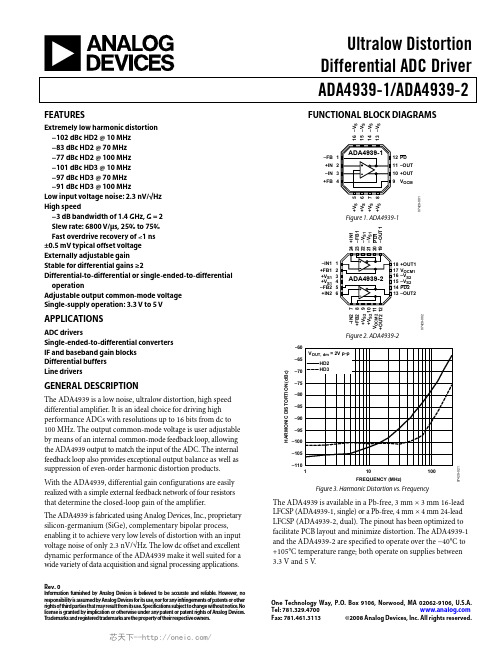
Ultralow DistortionDifferential ADC DriverADA4939-1/ADA4939-2 Rev. 0Information furnished by Analog Devices is believed to be accurate and reliable. However, noresponsibility is assumed by Analog Devices for its use, nor for any infringements of patents or other rights of third parties that may result from its use. Specifications subject to change without notice. No license is granted by implication or otherwise under any patent or patent rights of Analog Devices. T rademarks and registered trademarks are the property of their respective owners. One Technology Way, P.O. Box 9106, Norwood, MA 02062-9106, U.S.A. Tel: 781.329.4700 Fax: 781.461.3113 ©2008 Analog Devices, Inc. All rights reserved.FEATURESExtremely low harmonic distortion−102 dBc HD2 @ 10 MHz−83 dBc HD2 @ 70 MHz−77 dBc HD2 @ 100 MHz−101 dBc HD3 @ 10 MHz−97 dBc HD3 @ 70 MHz−91 dBc HD3 @ 100 MHzLow input voltage noise: 2.3 nV/√HzHigh speed−3 dB bandwidth of 1.4 GHz, G = 2Slew rate: 6800 V/μs, 25% to 75%Fast overdrive recovery of <1 ns±0.5 mV typical offset voltageExternally adjustable gainStable for differential gains ≥2Differential-to-differential or single-ended-to-differential operationAdjustable output common-mode voltageSingle-supply operation: 3.3 V to 5 VAPPLICATIONSADC driversSingle-ended-to-differential convertersIF and baseband gain blocksDifferential buffersLine driversGENERAL DESCRIPTIONThe ADA4939 is a low noise, ultralow distortion, high speed differential amplifier. It is an ideal choice for driving high performance ADCs with resolutions up to 16 bits from dc to 100 MHz. The output common-mode voltage is user adjustable by means of an internal common-mode feedback loop, allowing the ADA4939 output to match the input of the ADC. The internal feedback loop also provides exceptional output balance as well as suppression of even-order harmonic distortion products.With the ADA4939, differential gain configurations are easily realized with a simple external feedback network of four resistors that determine the closed-loop gain of the amplifier.The ADA4939 is fabricated using Analog Devices, Inc., proprietary silicon-germanium (SiGe), complementary bipolar process, enabling it to achieve very low levels of distortion with an input voltage noise of only 2.3 nV/√Hz. The low dc offset and excellent dynamic performance of the ADA4939 make it well suited for a wide variety of data acquisition and signal processing applications.FUNCTIONAL BLOCK DIAGRAMS1–FB2+IN3–IN4+FB11–OUT12PD10+OUT9V OCM5+VS6+VS7+VS8+VS15–VS16–VS14–VS13–VS7429-1Figure 1. ADA4939-11–IN12+FB13+V S14+V S15–FB26+IN27–IN28+FB29+VS211VOCM212+OUT21+VS217429-2Figure 2. ADA4939-2–60–110–105–100–95–90–85–80–75–70–65110100 HARMONICDISTORTION(dBc)FREQUENCY (MHz)7429-21Figure 3. Harmonic Distortion vs. FrequencyThe ADA4939 is available in a Pb-free, 3 mm × 3 mm 16-lead LFCSP (ADA4939-1, single) or a Pb-free, 4 mm × 4 mm 24-lead LFCSP (ADA4939-2, dual). The pinout has been optimized to facilitate PCB layout and minimize distortion. The ADA4939-1 and the ADA4939-2 are specified to operate over the −40°C to +105°C temperature range; both operate on supplies between 3.3 V and 5 V.ADA4939-1/ADA4939-2Rev. 0 | Page 2 of 24TABLE OF CONTENTSFeatures..............................................................................................1 Applications.......................................................................................1 General Description.........................................................................1 Functional Block Diagrams.............................................................1 Revision History...............................................................................2 Specifications.....................................................................................3 5 V Operation...............................................................................3 3.3 V Operation............................................................................5 Absolute Maximum Ratings............................................................7 Thermal Resistance......................................................................7 Maximum Power Dissipation.....................................................7 ESD Caution..................................................................................7 Pin Configurations and Function Descriptions...........................8 Typical Performance Characteristics.............................................9 Test Circuits.....................................................................................15 Operational Description................................................................16 Definition of Terms....................................................................16 Theory of Operation......................................................................17 Analyzing an Application Circuit............................................17 Setting the Closed-Loop Gain..................................................17 Stable for Gains ≥2.....................................................................17 Estimating the Output Noise Voltage......................................17 Impact of Mismatches in the Feedback Networks.................18 Calculating the Input Impedance for an Application Circuit .......................................................................................................19 Input Common-Mode Voltage Range.....................................21 Input and Output Capacitive AC-Coupling...........................21 Minimum R G Value of 50 Ω......................................................21 Setting the Output Common-Mode Voltage..........................21 Layout, Grounding, and Bypassing..............................................22 High Performance ADC Driving.................................................23 Outline Dimensions.......................................................................24 Ordering Guide.. (24)REVISION HISTORY5/08—Revision 0: Initial VersionADA4939-1/ADA4939-2Rev. 0 | Page 3 of 24SPECIFICATIONS5 V OPERATIONT A = 25°C, +V S = 5 V , −V S = 0 V , V OCM = +V S /2, R F = 402 Ω, R G = 200 Ω, R T = 60.4 Ω (when used), R L, dm = 1 kΩ, unless otherwise noted. All specifications refer to single-ended input and differential outputs, unless otherwise noted. Refer to Figure 42 for signal definitions.±D IN to V OUT, dm PerformanceTable 1.Parameter Conditions Min Typ Max Unit DYNAMIC PERFORMANCE −3 dB Small Signal Bandwidth V OUT, dm = 0.1 V p-p 1400 MHz Bandwidth for 0.1 dB Flatness V OUT, dm = 0.1 V p-p, ADA4939-1 300 MHz V OUT, dm = 0.1 V p-p, ADA4939-2 90 MHz Large Signal Bandwidth V OUT, dm = 2 V p-p 1400 MHz Slew Rate V OUT, dm = 2 V p-p, 25% to 75% 6800 V/μs Overdrive Recovery Time V IN = 0 V to 1.5 V step, G = 3.16 <1 ns NOISE/HARMONIC PERFORMANCE See Figure 41 for distortion test circuit Second Harmonic V OUT, dm = 2 V p-p, 10 MHz −102 dBc V OUT, dm = 2 V p-p, 70 MHz −83 dBc V OUT, dm = 2 V p-p, 100 MHz −77 dBc Third Harmonic V OUT, dm = 2 V p-p, 10 MHz −101 dBc V OUT, dm = 2 V p-p, 70 MHz −97 dBc V OUT, dm = 2 V p-p, 100 MHz−91 dBc IMD f 1 = 70 MHz, f 2 = 70.1 MHz, V OUT, dm = 2 V p-p −95 dBc f 1 = 140 MHz, f 2 = 140.1 MHz, V OUT, dm = 2 V p-p −89 dBc Voltage Noise (RTI) f = 100 kHz 2.3 nV/√Hz Input Current Noise f = 100 kHz 6 pA/√Hz Crosstalk f = 100 MHz, ADA4939-2 −80 dB INPUT CHARACTERISTICS Offset Voltage V OS, dm = V OUT, dm /2, V DIN+ = V DIN− = 2.5 V −3.4 ±0.5 +2.8 mV T MIN to T MAX variation ±2.0 μV/°C Input Bias Current −26 −10 +2.2 μA T MIN to T MAX variation ±0.5 μA/°C Input Offset Current −11.2 +0.5 +11.2 μA Input Resistance Differential 180 kΩ Common mode 450 kΩ Input Capacitance 1 pF Input Common-Mode Voltage1.1 3.9 V CMRR ∆V OUT, dm /∆V IN, cm , ∆V IN, cm = ±1 V −83 −77 dB OUTPUT CHARACTERISTICS Output Voltage Swing Maximum ∆V OUT ; single-ended output, R F = R G = 10 kΩ 0.9 4.1 V Linear Output Current 100 mA Output Balance Error ∆V OUT, cm /∆V OUT, dm , ∆V OUT, dm = 1 V, 10 MHz,see Figure 40 for test circuit−64 dBADA4939-1/ADA4939-2Rev. 0 | Page 4 of 24V OCM to V OUT, cm PerformanceTable 2.Parameter Conditions Min Typ Max Unit V OCM DYNAMIC PERFORMANCE −3 dB Bandwidth 670 MHz Slew Rate V IN = 1.5 V to 3.5 V, 25% to 75% 2500 V/μs Input Voltage Noise (RTI) f = 100 kHz 7.5 nV/√Hz V OCM INPUT CHARACTERISTICS Input Voltage Range 1.3 3.5 V Input Resistance 8.3 9.7 11.5 kΩ Input Offset Voltage V OS, cm = V OUT, cm , V DIN+ = V DIN− = +V S /2 −3.7 ±0.5 +3.7 mV V OCM CMRR ΔV OUT, dm /ΔV OCM , ΔV OCM = ±1 V −90 −73 dB Gain ΔV OUT, cm /ΔV OCM , ΔV OCM = ±1 V 0.97 0.98 0.99 V/VGeneral PerformanceADA4939-1/ADA4939-2Rev. 0 | Page 5 of 243.3 V OPERATIONT A = 25°C, +V S = 3.3 V , −V S = 0 V , V OCM = +V S /2, R F = 402 Ω, R G = 200 Ω, R T = 60.4 Ω (when used), R L, dm = 1 kΩ, unless otherwise noted. All specifications refer to single-ended input and differential outputs, unless otherwise noted. Refer to Figure 42 for signal definitions.±D IN to V OUT, dm PerformanceTable 4.Parameter Conditions Min Typ Max Unit DYNAMIC PERFORMANCE −3 dB Small Signal Bandwidth V OUT, dm = 0.1 V p-p 1400 MHz Bandwidth for 0.1 dB Flatness V OUT, dm = 0.1 V p-p, ADA4939-1 300 MHz V OUT, dm = 0.1 V p-p, ADA4939-2 90 MHz Large Signal Bandwidth V OUT, dm = 2 V p-p 1400 MHz Slew Rate V OUT, dm = 2 V p-p, 25% to 75% 5000 V/μs Overdrive Recovery Time V IN = 0 V to 1.0 V step, G = 3.16 <1 ns NOISE/HARMONIC PERFORMANCE See Figure 41 for distortion test circuit Second Harmonic V OUT, dm = 2 V p-p, 10 MHz −100 dBc V OUT, dm = 2 V p-p, 70 MHz −90 dBc V OUT, dm = 2 V p-p, 100 MHz −83 dBc Third Harmonic V OUT, dm = 2 V p-p, 10 MHz −94 dBc V OUT, dm = 2 V p-p, 70 MHz −82 dBc V OUT, dm = 2 V p-p, 100 MHz−75 dBc IMD f 1 = 70 MHz, f 2 = 70.1 MHz, V OUT, dm = 2 V p-p −87 dBc f 1 = 140 MHz, f 2 = 140.1 MHz, V OUT, dm = 2 V p-p −70 dBc Voltage Noise (RTI) f = 100 kHz 2.3 nV/√Hz Input Current Noise f = 100 kHz 6 pA/√Hz Crosstalk f = 100 MHz, ADA4939-2 −80 dB INPUT CHARACTERISTICS Offset Voltage V OS, dm = V OUT, dm /2, V DIN+ = V DIN− = +V S /2 −3.5 ±0.5 +3.5 mV T MIN to T MAX variation ±2.0 μV/°C Input Bias Current −26 −10 +2.2 μA T MIN to T MAX variation ±0.5 μA/°C Input Offset Current −11.2 ±0.4 +11.2 Input Resistance Differential 180 kΩ Common mode 450 kΩ Input Capacitance 1 pF Input Common-Mode Voltage0.9 2.4 V CMRR ∆V OUT, dm /∆V IN, cm , ∆V IN, cm = ±1 V −85 −75 dB OUTPUT CHARACTERISTICS Output Voltage Swing Maximum ∆V OUT , single-ended output, R F = R G = 10 kΩ 0.8 2.5 V Linear Output Current 75 mA Output Balance Error ∆V OUT, cm /∆V OUT, dm , ∆V OUT, dm = 1 V, f = 10 MHz,see Figure 40 for test circuit−61 dBADA4939-1/ADA4939-2Rev. 0 | Page 6 of 24V OCM to V OUT, cm PerformanceTable 5.Parameter Conditions Min Typ Max Unit V OCM DYNAMIC PERFORMANCE −3 dB Bandwidth 560 MHz Slew Rate V IN = 0.9 V to 2.4 V, 25% to 75% 1250 V/μs Input Voltage Noise (RTI) f = 100 kHz 7.5 nV/√Hz V OCM INPUT CHARACTERISTICS Input Voltage Range 1.3 1.9 V Input Resistance 8.3 9.7 11.2 kΩ Input Offset Voltage V OS, cm = V OUT, cm , V DIN+ = V DIN− = 1.67 V −3.7 ±0.5 +3.7 mV V OCM CMRR ∆V OUT, dm /∆V OCM , ∆V OCM = ±1 V −75 −73 dB Gain ∆V OUT, cm /∆V OCM , ∆V OCM = ±1 V0.97 0.98 0.99 V/VGeneral PerformanceADA4939-1/ADA4939-2Rev. 0 | Page 7 of 24ABSOLUTE MAXIMUM RATINGSStresses above those listed under Absolute Maximum Ratings may cause permanent damage to the device. This is a stress rating only; functional operation of the device at these or any other conditions above those indicated in the operational section of this specification is not implied. Exposure to absolute maximum rating conditions for extended periods may affect device reliability.THERMAL RESISTANCEθJA is specified for the device (including exposed pad) soldered to a high thermal conductivity 2s2p circuit board, as described in EIA/JESD 51-7.Table 8. Thermal ResistancePackage TypeθJA Unit ADA4939-1, 16-Lead LFCSP (Exposed Pad) 98 °C/W ADA4939-2, 24-Lead LFCSP (Exposed Pad)67 °C/WMAXIMUM POWER DISSIPATIONThe maximum safe power dissipation in the ADA4939 package is limited by the associated rise in junction temperature (T J ) on the die. At approximately 150°C, which is the glass transition temperature, the plastic changes its properties. Even temporarily exceeding this temperature limit can change the stresses that the package exerts on the die, permanently shifting the parametric performance of the ADA4939. Exceeding a junction temperature of 150°C for an extended period can result in changes in the silicon devices, potentially causing failure.The power dissipated in the package (P D ) is the sum of the quiescent power dissipation and the power dissipated in the package due to the load drive. The quiescent power is the voltage between the supply pins (V S ) times the quiescent current (I S ). The power dissipated due to the load drive depends upon the particular application. The power due to load drive is calculated by multiplying the load current by the associated voltage drop across the device. RMS voltages and currents must be used in these calculations.Airflow increases heat dissipation, effectively reducing θJA . In addition, more metal directly in contact with the package leads/ exposed pad from metal traces, through holes, ground, and power planes reduces θJA .Figure 4 shows the maximum safe power dissipation in the package vs. the ambient temperature for the single 16-lead LFCSP (98°C/W) and the dual 24-lead LFCSP (67°C/W) on a JEDEC standard four-layer board with the exposed pad soldered to a PCB pad that is connected to a solid plane.3.02.52.01.51.00.50–40100806040200–20M A X I M U MP O W E R D I S S I P A T I O N (W )AMBIENT TEMPERATURE (°C)07429-004Figure 4. Maximum Power Dissipation vs. Ambient Temperature fora Four-Layer BoardESD CAUTIONADA4939-1/ADA4939-2Rev. 0 | Page 8 of 24PIN CONFIGURATIONS AND FUNCTION DESCRIPTIONS1–FB 2+IN 3–IN 4+FB5+V S 6+V S 7+V S 8+V S 15–V S16–V S14–V S13–V S07429-005Figure 5. ADA4939-1 Pin Configuration123456789111210–IN1+FB1+V S1+V S1–FB2+IN2–I N 2+F B 2+VS 2V O C M 2+O U T 2+V S 2107429-006Figure 6. ADA4939-2 Pin ConfigurationADA4939-1/ADA4939-2Rev. 0 | Page 9 of 24TYPICAL PERFORMANCE CHARACTERISTICST A = 25°C, +V S = 5 V , −V S = 0 V , V OCM = +V S /2, R G = 200 Ω, R F = 402 Ω, R T = 60.4 Ω, G = 1, R L, dm = 1 kΩ, unless otherwise noted. Refer to Figure 39 for test setup. Refer to Figure 42 for signal definitions.2–14–12–10–8–6–4–201101001kN O R M A L I Z E D C L O S E D -L O O P G A I N (d B )FREQUENCY (MHz)07429-007Figure 7. Small Signal Frequency Response for Various Gains3–12–10–8–6–4–202–11–9–7–5–3–111101001kN O R M A L I Z E D C L O S E D -L OO P G A I N (d B )FREQUENCY (MHz)07429-008Figure 8. Small Signal Frequency Response for Various Supplies3–12–10–8–6–4–202–11–9–7–5–3–111101001kN O R M A L I Z E D C L O S E D -L OO P G A I N (d B )FREQUENCY (MHz)07429-009Figure 9. Small Signal Frequency Response for Various Temperatures2–14–12–10–8–6–4–201101001kN O R M A L I Z E D C L O S E D -L O O P G A I N (d B )FREQUENCY (MHz)07429-010Figure 10. Large Signal Frequency Response for Various Gains2–12–10–8–6–4–201101001kN O R M A L I Z E D C L O S E D-L O O P G A I N (d B )FREQUENCY (MHz)07429-011Figure 11. Large Signal Frequency Response for Various Supplies3–12–10–8–6–4–202–11–9–7–5–3–111101001kN O R M A L I Z E D C L O S E D-L O O P G A I N (d B )FREQUENCY (MHz)07429-012Figure 12. Large Signal Frequency Response for Various TemperaturesADA4939-1/ADA4939-2Rev. 0 | Page 10 of 243–12–10–8–6–4–202–11–9–7–5–3–111101001kN O R M A L I Z E D C L O S E D -L O O P G A I N (d B )FREQUENCY (MHz)07429-013Figure 13. Small Signal Frequency Response for Various Loads6–9–6–3301101001kV O C M G A I N (d B )FREQUENCY (MHz)07429-019Figure 14. V OCM Small Signal Frequency Response at Various DC Levels0.5–0.5–0.4–0.3–0.2–0.100.10.20.30.41101001kN O R M A L I Z E D C L O S E D -L O O P G A I N (d B )FREQUENCY (MHz)07429-020Figure 15. 0.1 dB Flatness Small Signal Response for Various Loads3–12–10–8–6–4–202–11–9–7–5–3–111101001kN O R M A L I Z E D C L O S E D -L OO P G A I N (d B )FREQUENCY (MHz)07429-016Figure 16. Large Signal Frequency Response for Various Loads–55–115–110–105–100–95–90–85–80–75–70–65–60110100H A R M O NI C D I S T O R T I O N (d B c )FREQUENCY (MHz)07429-022Figure 17. Harmonic Distortion vs. Frequency at Various Gains–60–110–105–100–95–90–85–80–75–70–65110100H A R M O N I C D I S T O RT I O N (d B c )FREQUENCY (MHz)07429-023Figure 18. Harmonic Distortion vs. Frequency at Various Loads–60–110–105–100–95–90–85–80–75–70–65110100H A R M O N I C D I S T O R T I O N (d B c )FREQUENCY (MHz)07429-062Figure 19. Harmonic Distortion vs. Frequency at Various Supplies–40–120–110–100–90–80–70–60–501.0 4.03.83.63.43.23.02.82.62.42.22.01.81.61.41.2D I S T O R T I O N (d B c )V OCM (V)07429-025Figure 20. Harmonic Distortion vs. V OCM at Various Frequencies–40–130–120–110–100–90–80–70–60–501.21.41.6 1.82D I S T O R T I O N (d B c )V OCM (V).007429-026Figure 21. Harmonic Distortion vs. V OCM at Various Frequencies–40–130–120–110–100–90–80–70–60–5007654321D I S T O R T I O N (d B c )V OUT, dm(V p-p)07429-024Figure 22. Harmonic Distortion vs. V OUT, dm and Supply Voltage, f = 10 MHz10–110–100–90–80–70–60–50–40–30–20–10069.570.570.470.370.270.170.069.969.869.769.6N O R M A L I Z E D S P E C T R U M(d B c )FREQUENCY (MHz)07429-028Figure 23. 70 MHz Intermodulation Distortion–30–35–40–45–50–55–60–65–70110100C M RR (d B )FREQUENCY (MHz)1k07429-029Figure 24. CMRR vs. Frequency–60–120–110–100–90–80–70110100H A R M O N I C D I S T O R T I O N (d B c )FREQUENCY (MHz)07429-027Figure 25. Harmonic Distortion vs. Frequency at Various Output Voltages–30–40–50–60–70–80–90–100110100P S R R (d B )FREQUENCY (MHz)1k07429-031Figure 26. PSRR vs. Frequency, RL = 200 Ω0–5–50–45–40–35–30–25–20–15–101101001kS -P A R A M E T E R S (d B )FREQUENCY (MHz)07429-032Figure 27. Return Loss (S11, S22) vs. Frequency–30–35–40–45–50–55–60–65–70110100O U T P U T B A L A N C E (d B )FREQUENCY (MHz)1k07429-030Figure 28. Output Balance vs. Frequency70–10100–350–300–250–200–150–100–505001020304050600.0110k1k1001010.1G A I N (d B )P H A S E (D e g r e e s )FREQUENCY (MHz)07429-034Figure 29. Open-Loop Gain and Phase vs. Frequency8–8–6–4–20246065040302010V O L T A G E (V )TIME (ns)07429-035Figure 30. Overdrive Recovery, G = 3.16–60–105–100–95–90–85–80–75–70–65110100S P U R I O U S -F R E E D Y N A M I C R A N G E (d B c )FREQUENCY (MHz)07429-033Figure 31. Spurious-Free Dynamic Range vs. Frequency at Various Loads0.120.100.080.060.040.020–0.0210987654321O U T P U T VO L T A G E (V )TIME (ns)07429-038Figure 32. Small Signal Pulse Response2.602.402.452.502.552018161412108642O U T P U T C O M M O N -M O D EV O L T A G E (V )TIME (ns)07429-039Figure 33. V OCM Small Signal Pulse Response–40–140–130–120–110–100–90–80–70–60–501110010C R O S S T A L K (d B)FREQUENCY (MHz)k07429-044Figure 34. Crosstalk vs. Frequency for ADA4939-24–4–3–2–10123010987654321O U T P U TV O L T A G E (V )TIME (ns)07429-041Figure 35. Large Signal Pulse Response4.50.51.01.52.02.53.03.54.002018161412108642O U T P U T C O M M O N -M O D EV O L T A G E (V )TIME (ns)07429-042Figure 36. V OCM Large Signal Pulse Response3.5–0.500.51.01.52.02.53.001000900800700600500400300200100V O L T A G E (V )TIME (ns)07429-0431k1101001010M1M 100k 10k 1k 100I N P U T V O L T A G E N O I S E (n V H z )FREQUENCY (Hz)07429-045Figure 37. PD Response TimeFigure 38. Voltage Noise Spectral Density, RTITEST CIRCUITS07429-046Figure 39. Equivalent Basic Test Circuit, G = 2NETWORK 07429-047Figure 40. Test Circuit for Output Balance, CMRRFigure 41. Test Circuit for Distortion MeasurementsOPERATIONAL DESCRIPTIONDEFINITION OF TERMS+D IN –FB+FB–D INV OCM 07429-049Figure 42. Circuit DefinitionsDifferential VoltageDifferential voltage refers to the difference between twonode voltages. For example, the output differential voltage (or equivalently, output differential-mode voltage) is defined asV OUT, dm = (V +OUT − V −OUT )where V +OUT and V −OUT refer to the voltages at the +OUT and −OUT terminals with respect to a common reference.Common-Mode VoltageCommon-mode voltage refers to the average of two node voltages. The output common-mode voltage is defined asV OUT, cm = (V +OUT + V −OUT )/2BalanceOutput balance is a measure of how close the differential signals are to being equal in amplitude and opposite in phase. Output balance is most easily determined by placing a well-matched resistor divider between the differential voltage nodes and comparing the magnitude of the signal at the divider midpoint with the magnitude of the differential signal (see Figure 39). By this definition, output balance is the magnitude of the output common-mode voltage divided by the magnitude of the output differential mode voltage.dmOUT cm OUT V V Error Balance Output ,,=THEORY OF OPERATIONThe ADA4939 differs from conventional op amps in that it has two outputs whose voltages move in opposite directions and an additional input, V OCM. Like an op amp, it relies on high open-loop gain and negative feedback to force these outputs to the desired voltages. The ADA4939 behaves much like a standard voltage feedback op amp and facilitates single-ended-to-differential conversions, common-mode level shifting, and amplifications of differential signals. Like an op amp, the ADA4939 has high input impedance and low output impedance. Because it uses voltage feedback, the ADA4939 manifests a nominally constant gain-bandwidth product.Two feedback loops are employed to control the differential and common-mode output voltages. The differential feedback, set with external resistors, controls only the differential output voltage. The common-mode feedback controls only the common-mode output voltage. This architecture makes it easy to set the output common-mode level to any arbitrary value within the specified limits. The output common-mode voltage is forced, by the internal common-mode feedback loop, to be equal to the voltage applied to the V OCM input.The internal common-mode feedback loop produces outputs that are highly balanced over a wide frequency range without requiring tightly matched external components. This results in differential outputs that are very close to the ideal of being identical in amplitude and are exactly 180° apart in phase. ANALYZING AN APPLICATION CIRCUITThe ADA4939 uses high open-loop gain and negative feedback to force its differential and common-mode output voltages in such a way as to minimize the differential and common-mode error voltages. The differential error voltage is defined as the voltage between the differential inputs labeled +IN and −IN (see Figure 42). For most purposes, this voltage can be assumed to be zero. Similarly, the difference between the actual output common-mode voltage and the voltage applied to V OCM can also be assumed to be zero. Starting from these two assumptions, any application circuit can be analyzed. SETTING THE CLOSED-LOOP GAINThe differential-mode gain of the circuit in Figure 42 can be determined byGFdmINdmOUTRRVV=,,This presumes that the input resistors (R G) and feedback resistors (R F) on each side are equal.STABLE FOR GAINS ≥2The ADA4939 frequency response exhibits excessive peaking for differential gains <2; therefore, the part should be operated with differential gains ≥2.ESTIMATING THE OUTPUT NOISE VOLTAGEThe differential output noise of the ADA4939 can be estimated using the noise model in Figure 43. The input-referred noise voltage density, v nIN, is modeled as a differential input, and the noise currents, i nIN− and i nIN+, appear between each input and ground. The output voltage due to v nIN is obtained by multiplying v nIN by the noise gain, G N (defined in the G N equation that follows). The noise currents are uncorrelated with the same mean-square value, and each produces an output voltage that is equal to the noise current multiplied by the associated feedback resistance. The noise voltage density at the V OCM pin is v nCM. When the feedback networks have the same feedback factor, as in most cases, the output noise due to v nCM is common-mode. Each of the four resistors contributes (4kTR xx)1/2. The noise from the feedback resistors appears directly at the output, and the noise from the gain resistors appears at the output multiplied by R F/R G. Table 11 summarizes the input noise sources, the multiplication factors, and the output-referred noise density terms.VV7429-5Figure 43. Noise ModelTable 11. Output Noise Voltage Density Calculations for Matched Feedback NetworksInput Noise ContributionInput Noise Term Input Noise Voltage Density Output Multiplication Factor Differential Output Noise Voltage Density Term Differential Input v nIN v nIN G N v nO1 = G N (v nIN ) Inverting Input i nIN i nIN × (R F2) 1 v nO2 = (i nIN )(R F2) Noninverting Input i nIN i nIN × (R F1) 1 v nO3 = (i nIN )(R F1) V OCM Inputv nCM v nCM 0 v nO4 = 0Gain Resistor R G1v nRG1(4kTR G1)1/2R F1/R G1v nO5 = (R F1/R G1)(4kTR G1)1/2Gain Resistor R G2v nRG2(4kTR G2)1/2R F2/R G2v nO6 = (R F2/R G2)(4kTR G2)1/2Feedback Resistor R F1v nRF1(4kTR F1)1/2 1 v nO7 = (4kTR F1)1/2Feedback Resistor R F2v nRF2(4kTR F2)1/2 1 v nO8 = (4kTR F2)1/2Table 12. Differential Input, DC-CoupledNominal Gain (dB) R F (Ω) R G (Ω) R IN, dm (Ω) Differential Output Noise Density (nV/√Hz) 6 402 200 400 9.7 10 402 127 254 12.4 14 402 80.6 161 16.6Table 13. Single-Ended Ground-Referenced Input, DC-Coupled, R S = 50 ΩNominal Gain (dB) R F (Ω) R G1 (Ω) R T (Ω) R IN, cm (Ω) R G2 (Ω)1Differential Output Noise Density (nV/√Hz) 6 402 200 60.4 301 228 9.1 10 402 127 66.5 205 155 11.1 14 402 80.6 76.8 138 111 13.5G2G1S TSimilar to the case of a conventional op amp, the output noise voltage densities can be estimated by multiplying the input-referred terms at +IN and −IN by the appropriate output factor, where:()21N ββG +=2is the circuit noise gain.G1F1G11R R R β+= and G2F2G22R R R β+=are the feedback factors.When the feedback factors are matched, R F1/R G1 = R F2/R G2, β1 = β2 = β, and the noise gain becomesGF N R R βG +==11 Note that the output noise from V OCM goes to zero in this case.The total differential output noise density, v nOD , is the root-sum-square of the individual output noise terms.∑==81i 2nOi nOD v vTable 12 and Table 13 list several common gain settings,associated resistor values, input impedance, and output noise density for both balanced and unbalanced input configurations.IMPACT OF MISMATCHES IN THE FEEDBACK NETWORKSAs previously mentioned, even if the external feedback networks (R F /R G ) are mismatched, the internal common-mode feedback loop still forces the outputs to remain balanced. The amplitudes of the signals at each output remain equal and 180° out of phase. The input-to-output differential mode gain varies proportionately to the feedback mismatch, but the output balance is unaffected. The gain from the V OCM pin to V O, dm is equal to2(β1 − β2)/(β1 + β2)When β1 = β2, this term goes to zero and there is no differential output voltage due to the voltage on the V OCM input (including noise). The extreme case occurs when one loop is open and the other has 100% feedback; in this case, the gain from V OCM input to V O, dm is either +2 or −2, depending on which loop is closed. The feedback loops are nominally matched to within 1% in most applications, and the output noise and offsets due to the V OCM input are negligible. If the loops are intentionally mismatched by a large amount, it is necessary to include the gain term from V OCM to V O, dm and account for the extra noise. For example, if β1 = 0.5 and β2 = 0.25, the gain from V OCM to V O, dm is 0.67. If the V OCM pin is set to 2.5 V , a differential offset voltage is present at the output of (2.5 V)(0.67) = 1.67 V . The differential output noise contribution is (7.5 nV/√Hz)(0.67) = 5 nV/√Hz. Both of these results are undesirable in most applications; therefore, it is best to use nominally matched feedback factors.。
ADA4817-1中文资料
FEATURES
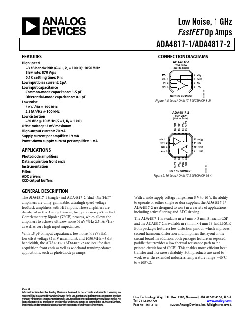
High speed −3 dB bandwidth (G = 1, RL = 100 Ω): 1050 MHz Slew rate: 870 V/μs 0.1% settling time: 9 ns
Low input bias current: 2 pA Low input capacitance
NC = NO CONNECT
Figure 1. 8-Lead ADA4817-1 LFCSP (CP-8-2)
ADA4817-2
TOP VIEW (Not to Scale)
16 FB1 15 PD1 14 +VS1 13 OUT1
–IN1 1 +IN1 2
NC 3 –VS2 4
12 –VS1 11 NC 10 +IN2 9 –IN2
Low Noise, 1 GHz FastFET Op Amps ADA4817-1/ADA4817-2
CONNECTION DIAGRAMS
ADA4817-1
TOP VIEW (Not to Scale)
PD 1 FB 2 –T 6 NC 5 –VS
07756-001
元器件交易网
ADA4817-1/ADA4817-2
TABLE OF CONTENTS
Features .............................................................................................. 1 Applications....................................................................................... 1 Connection Diagrams...................................................................... 1 General Description ......................................................................... 1 Revision History ............................................................................... 2 Specifications..................................................................................... 3
ADA4899-1_07中文资料

HARMONIC DISTORTION (dBc)
–60 –70 –80 –90
HD3 HD2
–100 –110
05720-071
–120 –130 0.1
1
10 FREQUENCY (MHz)
100
Figure 3. Harmonic Distortion vs. Frequency
元器件交易网
ADA4899-1 TABLE OF CONTENTS
Features .............................................................................................. 1 Applications....................................................................................... 1 Connection Diagrams...................................................................... 1 General Description ......................................................................... 1 Revision History ............................................................................... 2 Specifications with ±5 V Supply ..................................................... 3 Specifications with +5 V Supply ..................................................... 4 Absolute Maximum Ratings............................................................ 5 Maximum Power Dissipation ..................................................... 5 ESD Caution.................................................................................. 5 Typical Performance Characteristics ............................................. 6 Test Circuits..................................................................................... 12 Theory of Operation ...................................................................... 13 Packaging Innovation ................................................................ 13 DISABLE Pin .............................................................................. 13 Applications..................................................................................... 14 Unity Gain Operation................................................................ 14 Recommended Values for Various Gains................................ 14 Noise ............................................................................................ 15 ADC Driver................................................................................. 15 DISABLE Pin Operation ........................................................... 16 ADA4899-1 Mux ........................................................................ 16 Circuit Considerations .............................................................. 16 Outline Dimensions ....................................................................... 18 Ordering Guide .......................................................................... 18
ADA4938-1中文资料

Ultra-Low Distortion Differential ADC DriverPreliminary Technical DataADA4938-1Rev. PrAnformation furnished by Analog Devices is believed to be accurate and reliable. However , no responsibility is assumed by Analog Devices for its use, nor for any infringements of patents or other rights of third parties that may result from its use. Specifications subject to change without notice. No license is granted by implication or otherwise under any patent or patent rights of Analog Devices. T rademarks and registered trademarks are the property of their respective owners.One Technology Way, P.O. Box 9106, Norwood, MA 02062-9106, U.S.A.Tel: 781.329.4700 Fax: 781.461.3113 ©2006 Analog Devices, Inc. All rights reserved.FEATURESExtremely low harmonic distortion −108 dBc HD2 @ 10 MHz −79 dBc HD2 @ 70 MHz −125 dBc HD3 @ 10 MHz −87 dBc HD3 @ 70 MHzLow input voltage noise: 2.2 nV/√Hz High speed−3 dB bandwidth of 1.5 GHz, G = 1 Slew rate: 4700 V/μs0.1 dB gain flatness to 125 MHz Fast settling to 0.01% in 8.5 ns Fast overdrive recovery of 4 ns 1 mV typical offset voltage Externally adjustable gainDifferential to differential or single-ended to differential operationAdjustable output common-mode voltage Wide Supply Voltage Range: +5 V & ± 5 V Pb-free 3 mm x 3 mm LFCSP packageAPPLICATIONSADC driversSingle-ended-to-differential converters IF and baseband gain blocksDifferential buffers Line driversFUNCTIONAL BLOCK DIAGRAMFigure 1.GENERAL DESCRIPTIONThe ADA4938-1 is a low noise, ultra-low distortion, high speed differential amplifier. It is an ideal choice for driving highperformance ADCs with resolutions up to 16 bits from dc to 70 MHz. The output common mode voltage is adjustable over a wide range, allowing the ADA4938-1 to match the input of the ADC. The internal common mode feedback loop also provides exceptional output balance as well as suppression of even-order harmonic distortion products.Full differential and single-ended to differential gainconfigurations are easily realized with the ADA4938-1. A simple external feedback network of four resistors determines the amplifier’s closed-loop gain. The ADA4938-1 is fabricated using ADI’s proprietary third generation high-voltage XFCB process, enabling it to achieve very low levels of distortion with input voltage noise of only 2.2 nV/√Hz. The low dc offset and excellent dynamic performance of the ADA4938-1 make it well suited for a wide variety of data acquisition and signal processing and applications. The ADA4938-1 is available in a Pb-free, 3 mm x 3mm lead frame chip scale package (LFCSP). It is specified to operate over the extended industrial temperature range of −40°C to +85°C.ADA4938-1Preliminary Technical DataRev. PrA | Page 2 of 9TABLE OF CONTENTSFeatures..............................................................................................1 Applications.......................................................................................1 Functional Block Diagram..............................................................1 General Description.........................................................................1 Revision History...............................................................................2 Specifications.....................................................................................3 Dual Supply Operation................................................................3 Single Supply Operation...............................................................5 Absolute Maximum Ratings............................................................7 Thermal Resistance.......................................................................7 ESD Caution...................................................................................7 Pin Configuration and Function Descriptions..............................8 Outline Dimensions..........................................................................9 Ordering Guide.. (9)REVISION HISTORY12/06—Revision PrA: Initial VersionPreliminary Technical DataADA4938-1Rev. PrA | Page 3 of 9SPECIFICATIONSDUAL SUPPLY OPERATIONAt 25 °C, +V S = 5 V , −V S = −5 V , V OCM = 0 V , R G = R F = 200 Ω, G = +1, R L, dm = 1 kΩ, unless otherwise noted. All specifications refer to single-ended input and differential outputs, unless otherwise noted. Table 1.Parameter Conditions Min Typ Max Unit ±D IN TO ±OUT PERFORMANCE DYNAMIC PERFORMANCE −3 dB Small Signal Bandwidth V OUT = 0.5 V p-p, Differential Input 1500 MHz Bandwidth for 0.1 dB Flatness V OUT = 2 V p-p, Differential Input 125 MHz Large Signal Bandwidth V OUT = 2 V p-p, Differential Input 1300 MHz V OUT = 4 V p-p, Differential Input 800 MHz Slew Rate V OUT = 2 V p-p 4700 V/μs Settling Time 0.01%, V OUT = 2 Vp-p 8.5 ns Overdrive Recovery Time V IN = 5 V to 0 V step, G = +2 4 nsNOISE/HARMONIC PERFORMANCE 1Second Harmonic V OUT = 2 V p-p, 10 MHz −108 dBc V OUT = 2 V p-p, 70 MHz −79 dBc Third Harmonic V OUT = 2 V p-p, 10 MHz −125 dBc V OUT = 2 V p-p, 70 MHz −87 dBc IMD 70 MHz dBc IP3 70 MHz dBm Voltage Noise (RTI) 2.2 nV/√Hz Noise Figure G = +2 12 dB Input Current Noise 2 pA/√Hz INPUT CHARACTERISTICS Offset Voltage V OS, dm = V OUT, dm /2; V DIN+ = V DIN− = 0 V 1 mV T MIN to T MAX variation ±4 μV/°C Input Bias Current 3.5 μA T MIN to T MAX variation −0.01 μA/°C Input Resistance Differential 6 MΩ Common mode 3 MΩ Input Capacitance 1 pF Input Common-Mode Voltage −4.7 to 3.4 V CMRR ∆V OUT, dm /∆V IN, cm ; ∆V IN, cm = ±1 V −77 dB OUTPUT CHARACTERISTICS Output Voltage Swing Maximum ∆V OUT ; single-ended output 1 4 V Output Current 95 mA Output Balance Error ∆V OUT, cm /∆V OUT, dm ; ∆V OUT, dm = 1 V; 10 MHz −66 dB V OCM to ±OUT PERFORMANCE V OCM DYNAMIC PERFORMANCE −3 dB Bandwidth 400 MHz Slew Rate 1700 V/μs INPUT VOLTAGE NOISE (RTI) 7.5 nV/√Hz V OCM INPUT CHARACTERISTICS Input Voltage Range −3.8 3.8 V Input Resistance 200 kΩ Input Offset Voltage V OS, cm = V OUT, cm ; V DIN+ = V DIN– = 0 V 1 3.5 mV Input Bias Current 0.5 μA V OCM CMRR ∆V OUT, dm /∆V OCM ; ∆V OCM = ±1 V −75 dB Gain ∆V OUT, cm /∆V OCM ; ∆V OCM = ±1 V 1 V/V POWER SUPPLYADA4938-1 Preliminary Technical DataRev. PrA | Page 4 of 9Preliminary Technical DataADA4938-1Rev. PrA | Page 5 of 9SINGLE SUPPLY OPERATIONAt 25 °C, +V S = 5 V , -V S = 0 V , V OCM = 2.5 V , R G = R F = 200 Ω, G = +1, R L , dm = 1 kΩ, unless otherwise noted. All specifications refer to single-ended input and differential output, unless otherwise noted. Table 2.Parameter Conditions Min Typ Max Unit ±D IN TO ±OUT PERFORMANCE DYNAMIC PERFORMANCE −3 dB Small Signal Bandwidth V OUT = 0.5 V p-p, Differential Input 1500 MHz Bandwidth for 0.1 dB Flatness V OUT = 2 V p-p, Differential Input 125 MHz Large Signal Bandwidth V OUT = 2 V p-p, Differential Input 1100 MHz Slew Rate V OUT = 2 V p-p 3900 V/μs Settling Time 0.01%, V OUT = 2 V p-p 8.1 ns Overdrive Recovery Time V IN = 2.5 V to 0 V step, G = +2 4 ns NOISE/HARMONIC PERFORMANCE Second Harmonic V OUT = 2 V p-p, 10 MHz −115 dBc V OUT = 2 V p-p, 70 MHz −87 dBc Third Harmonic V OUT = 2 V p-p, 10 MHz −110 dBc V OUT = 2 V p-p, 70 MHz −79 dBc IMD 70 MHz dBc IP3 70 MHz dBm Voltage Noise (RTI) 2.2 nV/√Hz Noise Figure G = +2 12 dB Input Current Noise 2 pA/√Hz INPUT CHARACTERISTICS Offset Voltage V OS, dm = V OUT, dm /2; V DIN+ = V DIN− = V OCM = 2.5 V 1 mV T MIN to T MAX variation ±4 μV/°C Input Bias Current 3.5 μA T MIN to T MAX variation −0.01 μA/°C Input Resistance Differential 6 MΩ Common mode 3 MΩ Input Capacitance 1 pF Input Common-Mode Voltage 0.3 to 3.4 V CMRR ∆V OUT, dm /∆V IN, cm ; ∆V IN, cm = ±1 V −77 dB OUTPUT CHARACTERISTICS Output Voltage Swing Maximum ∆V OUT ; single-ended output 1.1 3.9 V Output Current 95 mA Output Balance Error ∆V OUT, cm /∆V OUT, dm ; ∆V OUT, dm = 1 V −66 dB V OCM TO ±OUT PERFORMANCE V OCM DYNAMIC PERFORMANCE −3 dB Bandwidth 400 MHz Slew Rate V = 0.5 V 1700 V/μs INPUT VOLTAGE NOISE (RTI) nV/√Hz V OCM INPUT CHARACTERISTICS Input Voltage Range 1.2 3.8 V Input Resistance 200 kΩ Input Offset Voltage V OS, cm = V OUT, cm ; V DIN+ = V DIN– = V OCM = 2.5 V 1 mV Input Bias Current 0.5 μA V OCM CMRR ∆V OUT, dm /∆V OCM ; ∆V OCM = ±1 V −75 dB Gain ∆V OUT, cm /∆V OCM ; ∆V OCM = ±1 V 1 V/V POWER SUPPLY Operating Range 4.5 12 V Quiescent Current 36 mA T MIN to T MAX variation 40 μA/°CADA4938-1 Preliminary Technical DataRev. PrA | Page 6 of 9Preliminary Technical DataADA4938-1Rev. PrA | Page 7 of 9ABSOLUTE MAXIMUM RATINGSTable 3.Parameter Rating Supply Voltage TBDPower DissipationSee Figure 2Storage Temperature Range −65°C to +125°C Operating Temperature Range−40°C to +85°C Lead Temperature (Soldering, 10 sec) 300°C Junction Temperature150°CStresses above those listed under Absolute MaximumRating may cause permanent damage to the device. This is a stress rating only; functional operation of the device at these or any other conditions above those indicated in the operational section of this specification is not implied. Exposure to absolute maximum rating conditions for extended periods may affect device reliability.THERMAL RESISTANCEθJA is specified for the worst-case conditions; that is, θJA is specified for a device (including exposed pad) soldered to the circuit board.Table 4. Thermal ResistancePackage TypeθJA Unit 16-Lead LFCSP (Exposed Pad)TBD °C/WMaximum Power DissipationThe maximum safe power dissipation in the ADA4938-1 package is limited by the associated rise in junctiontemperature (T J ) on the die. At approximately 150°C, which is the glass transition temperature, the plastic changes its properties. Even temporarily exceeding this temperature limit can change the stresses that the package exerts on the die, permanently shifting the parametric performance of the ADA4938-1. Exceeding a junction temperature of 150°C for an extended period can result in changes in the silicon devices, potentially causing failure.The power dissipated in the package (P D) is the sum of the quiescent power dissipation and the power dissipated in the package due to the load drive. The quiescent power is the voltage between the supply pins (V S ) times the quiescentcurrent (I S ). The power dissipated due to the load drive depends upon the particular application. The power due to load drive is calculated by multiplying the load current by the associated voltage drop across the device. RMS voltages and currents must be used in these calculations.Airflow increases heat dissipation, effectively reducing θJA . In addition, more metal directly in contact with the package leads/exposed pad from metal traces, through-holes, ground, and power planes reduces the θJA .Figure 2 shows the maximum safe power dissipation in the package vs. the ambient temperature for the 16-lead LFCSP (TBD °C/W) on a JEDEC standard 4-layer board.Figure 2. Maximum Power Dissipation vs. Temperature for a 4-Layer BoardESD CAUTIONADA4938-1Preliminary Technical DataRev. PrA | Page 8 of 9PIN CONFIGURATION AND FUNCTION DESCRIPTIONS1FB -OUT2+IN3-IN4FB +OUT-OUTPD+OUT9VOCMFigure 3. Pin ConfigurationPreliminary Technical DataADA4938-1Rev. PrA | Page 9 of 9OUTLINE DIMENSIONS0.500.400.900.850.80*COMPLIANT TO JEDEC STANDARDS MO-220-VEED-2EXCEPT FOR EXPOSED PAD DIMENSION.Figure 4. 16-Lead Lead Frame Chip Scale Package [LFCSP_VQ]3 mm × 3 mm Body(CP-16-3)Dimensions shown in millimetersORDERING GUIDEModel Ordering Quantity Temperature Range Package Description Package OptionBranding ADA4938-1YCPZ-R2 5,000 −40°C to +85°C 16-Lead 3 mm × 3 mm LFCSP CP-16 -3 ADA4938-1YCPZ-RL 1,500 −40°C to +85°C 16-Lead 3 mm × 3 mm LFCSP CP-16 -3 ADA4938-1YCPZ-R7 250 −40°C to +85°C 16-Lead 3 mm × 3 mm LFCSPCP-16 -3©2006 Analog Devices, nc. All rights reserved. Trademarks and registered trademarks are the property of their respective owners. PR06592-0-12/06(PrA)。
ADA4627-1_4637-1_cn

2010年10月——修订版C至修订版D 更改图1和概述 .............................................................................. 1 更改“订购指南”............................................................................ 18 2010年7月——修订版B至C 增加ADA4637-1...................................................................... 通篇 增加图2;重新排序 ..................................................................... 1 更改表2 ........................................................................................... 3 更改表3 ........................................................................................... 5 更改“典型工作特性”部分 ........................................................... 6 更新“外形尺寸”............................................................................ 17 更改“订购指南”............................................................................ 18
ADI高速运算放大器
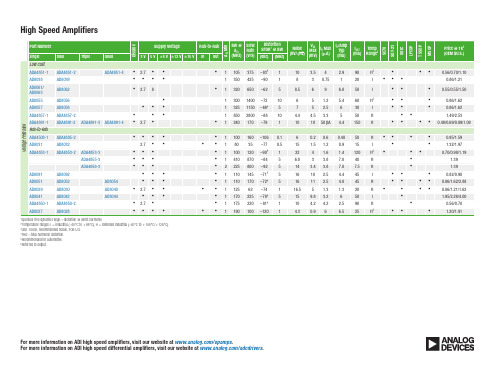
7 6.6 0.5 0.45 7 6.6
5 7 7.7 6.5 4.8 7
32 50 40 50 32 50
H I H H H/I I
• • • • • •
Spurious-free dynamic range—distortion @ worst harmonic. 2 Temperature ranges: I = industrial (–40°C to +85°C), H = extended industrial (–40°C to +105°C/+125°C). 3 USD 1000s, recommended resale, FOB U.S. 4 THD—total harmonic distortion. 5 Recommended for automotive. 6 Referred to output.
3 0.95 2.1 2 1 1 2.1 2.5 3 3.8 4.4 5.2 4 6.6 7 11 14 4.5 8 4.3
0.2 0.5 0.5 0.35 0.5 0.5 1 6 1 3 1 3 2 1 1.5 2 0.7 1 3 5
6 1 5.3 16 17 17 11.3 5 6.3 3.5 1.65 3.5 20 pA 5 pA 7 pA 11 pA 25 pA 2 7 15
•
0.56/0.70/1.10 0.86/1.21
• •
1 1 1 1
• • • • • • • •
0.55/0.55/1.50 0.86/1.62 0.86/1.62 1.49/2.53 0.49/0.69/0.89/1.09 0.95/1.59 1.32/1.97 0.70/0.98/1.19 1.39 1.39
- 1、下载文档前请自行甄别文档内容的完整性,平台不提供额外的编辑、内容补充、找答案等附加服务。
- 2、"仅部分预览"的文档,不可在线预览部分如存在完整性等问题,可反馈申请退款(可完整预览的文档不适用该条件!)。
- 3、如文档侵犯您的权益,请联系客服反馈,我们会尽快为您处理(人工客服工作时间:9:00-18:30)。
Ultralow Distortion,Differential ADC DriverADA4937-1 Rev. 0Information furnished by Analog Devices is believed to be accurate and reliable. However, noresponsibility is assumed by Analog Devices for its use, nor for any infringements of patents or other rights of third parties that may result from its use. Specifications subject to change without notice. No license is granted by implication or otherwise under any patent or patent rights of Analog Devices. T rademarks and registered trademarks are the property of their respective owners. One Technology Way, P.O. Box 9106, Norwood, MA 02062-9106, U.S.A. Tel: 781.329.4700 Fax: 781.461.3113 ©2007 Analog Devices, Inc. All rights reserved.FEATURESExtremely low harmonic distortion−112 dBc HD2 @ 10 MHz−79 dBc HD2 @ 70 MHz−70 dBc HD2 @ 100 MHz−102 dBc HD3 @ 10 MHz−91 dBc HD3 @ 70 MHz−84 dBc HD3 @ 100 MHzLow input voltage noise: 2.2 nV/√HzHigh speed−3 dB bandwidth of 1.9 GHz, G = 1Slew rate: 6000 V/μs, 25% to 75%0.1 dB gain flatness to 200 MHzFast overdrive recovery of 1 ns1 mV typical offset voltageExternally adjustable gainDifferential-to-differential or single-ended-to-differential operationAdjustable output common-mode voltageSingle-supply operation: 3.3 V to 5 VPb-free, 3 mm × 3 mm 16-lead LFCSPAPPLICATIONSADC driversSingle-ended-to-differential convertersIF and baseband gain blocksDifferential buffersLine driversFUNCTIONAL BLOCK DIAGRAM6591-11–FB2+IN3–IN4+FB11–OUT12PD10+OUT9V OCM5+VS6+VS7+VS8+VS15–VS16–VS14–VS13–VSFigure 1.–55–60–65–70–75–80–85–90–95–100–105–110–11511010DISTORTION(dBc)FREQUENCY (MHz)6591-2 Figure 2. Harmonic Distortion vs. FrequencyGENERAL DESCRIPTIONThe ADA4937-1 is a low noise, ultralow distortion, high speed differential amplifier. It is an ideal choice for driving high performance ADCs with resolutions up to 16 bits from dc to 100 MHz. The adjustable level of the output common mode allows the ADA4937-1 to match the input of the ADC. The internal common-mode feedback loop also provides exceptional output balance as well as suppression of even-order harmonic distortion products.With the ADA4937-1, differential gain configurations are easily realized with a simple external feedback network of four resistors determining the closed-loop gain of the amplifier. The ADA4937-1 is fabricated using Analog Devices, Inc. proprietary silicon-germanium (SiGe), complementary bipolar process, enabling it to achieve very low levels of distortion with an input voltage noise of only 2.2 nV/√Hz. The low dc offset and excellent dynamic performance of the ADA4937-1 make it well suited for a wide variety of data acquisition and signal processing applications.The ADA4937-1 is available in a Pb-free, 3 mm × 3 mm 16-lead LFCSP. The pinout has been optimized to facilitate PCB layout and minimize distortion. The part is specified to operate over the −40°C to +105°C temperature range for 3.3 V supplies and the −40°C to +85°C temperature range for 5 V supplies.ADA4937-1Rev. 0 | Page 2 of 28TABLE OF CONTENTSFeatures..............................................................................................1 Applications.......................................................................................1 Functional Block Diagram..............................................................1 General Description.........................................................................1 Revision History...............................................................................2 Specifications.....................................................................................3 5 V Operation...............................................................................3 3.3 V Operation............................................................................5 Absolute Maximum Ratings............................................................7 Thermal Resistance......................................................................7 ESD Caution..................................................................................7 Pin Configuration and Function Descriptions.............................8 Typical Performance Characteristics.............................................9 Test Circuits.....................................................................................16 Operational Description................................................................17 Definition of Terms....................................................................17 Theory of Operation......................................................................18 Analyzing an Application Circuit............................................18 Setting the Closed-Loop Gain..................................................18 Estimating the Output Noise Voltage......................................18 The Impact of Mismatches in the Feedback Networks.........19 Calculating the Input Impedance of an Application Circuit 19 Input Common-Mode Voltage Range in Single-SupplyApplications................................................................................19 Setting the Output Common-Mode Voltage..........................19 Layout, Grounding, and Bypassing..............................................21 High Performance ADC Driving.................................................22 3.3 V Operation..........................................................................24 Outline Dimensions.......................................................................25 Ordering Guide.. (25)REVISION HISTORY5/07—Revision 0: Initial VersionADA4937-1Rev. 0 | Page 3 of 28SPECIFICATIONS5 V OPERATIONT A = 25°C, +V S = 5 V , −V S = 0 V , V OCM = +V S /2, R T = 61.9 Ω, R G = R F = 200 Ω, G = 1, R L, dm = 1 kΩ, unless otherwise noted. All specifications refer to single-ended input and differential outputs, unless otherwise noted. Table 1. ±D IN to ±OUT PerformanceParameter Conditions Min Typ Max Unit DYNAMIC PERFORMANCE −3 dB Small Signal Bandwidth V OUT, dm = 0.1 V p-p 1900 MHz Bandwidth for 0.1 dB Flatness V OUT, dm = 0.1 V p-p 200 MHz Large Signal Bandwidth V OUT, dm = 2 V p-p 1700 MHz Slew Rate V OUT, dm = 2 V p-p; 25% to 75% 6000 V/μs Overdrive Recovery Time V IN = 0 V to 1.5 V step; G = 3.16 <1 ns NOISE/HARMONIC PERFORMANCE See Figure 45 for distortion test circuit Second Harmonic V OUT, dm = 2 V p-p; 10 MHz −112 dBc V OUT, dm = 2 V p-p;, 70 MHz −79 dBc V OUT, dm = 2 V p-p; 100 MHz −70 dBc Third Harmonic V OUT, dm = 2 V p-p; 10 MHz −102 dBc V OUT, dm = 2 V p-p; 70 MHz −91 dBc V OUT, dm = 2 V p-p; 100 MHz−84 dBc MD f 1 = 70 MHz; f 2 = 70.1 MHz; V OUT, dm = 2 V p-p −91 dBc Voltage Noise (RTI) f = 100 kHz 2.2 nV/√Hz Input Current Noise f = 100 kHz 3 pA/√Hz Noise Figure G = 4; R T = 136 Ω; R F = 200 Ω; R G = 37 Ω; f = 100 MHz 15 dB INPUT CHARACTERISTICS Offset Voltage V OS, dm = V OUT, dm /2; V DIN+ = V DIN− = 2.5 V −2.5 +0.5 +2.5 mV T MIN to T MAX variation ±1 μV/°C Input Bias Current −30 −20 −10 μA T MIN to T MAX variation 0.01 μA/°C Input Offset Current −2 +0.5 +2 μA Input Resistance Differential6 MΩ Common mode 3 MΩ Input Capacitance 1 pF Input Common-Mode Voltage0.3 to 3.0 V CMRR ∆V OUT, dm /∆V IN, cm ; ∆V IN, cm = ±1 V −67 −80 dB OUTPUT CHARACTERISTICS Output Voltage Swing Maximum ∆V OUT ; single-ended output; R F = R G = 10 kΩ 0.8 4.2 V Linear Output Current >100 mAOutput Balance Error ∆V OUT, cm /∆V OUT, dm ; ∆V OUT, dm = 1 V; 10 MHz;see Figure 44 for test circuit−61 dBADA4937-1Rev. 0 | Page 4 of 28ADA4937-1Rev. 0 | Page 5 of 283.3 V OPERATIONT A = 25°C, +V S = 3.3 V , −V S = 0 V , V OCM = +V S /2, R T = 61.9 Ω, R G = R F = 200 Ω, G = 1, R L, dm = 1 kΩ, unless otherwise noted. All specifications refer to single-ended input and differential outputs, unless otherwise noted. Table 3. ±D IN to ±OUT PerformanceParameter Conditions Min Typ Max Unit DYNAMIC PERFORMANCE −3 dB Small Signal Bandwidth V OUT, dm = 0.1 V p-p 1900 MHz Bandwidth for 0.1 dB Flatness V OUT, dm = 0.1 V p-p 200 MHz Large Signal Bandwidth V OUT , dm = 2 V p-p 1300 MHz Slew Rate V OUT, dm = 2 V p-p; 25% to 75% 4000 V/μs Overdrive Recovery Time V IN = 0 V to 1.0 V step; G = 3.16 <1 ns NOISE/HARMONIC PERFORMANCE See Figure 45 for distortion test circuit Second Harmonic V OUT, dm = 2 V p-p; 10 MHz −106 dBc V OUT, dm = 2 V p-p; 70 MHz −88 dBc V OUT, dm = 2 V p-p; 100 MHz −81 dBc Third Harmonic V OUT, dm = 2 V p-p; 10 MHz −93 dBc V OUT, dm = 2 V p-p; 70 MHz −80 dBc V OUT, dm = 2 V p-p; 100 MHz −71 dBc MD f 1 = 70 MHz; f 2 = 70.1 MHz; V OUT , dm = 2 V p-p −87 dBc Voltage Noise (RTI) f = 100 kHz 2.2 nV/√Hz Input Current Noise f = 100 kHz 3 pA/√Hz Noise Figure G = 4; R T = 136 Ω; R F = 200 Ω; R G = 37 Ω; f = 100 MHz 15 dB INPUT CHARACTERISTICS Offset Voltage V OS, dm = V OUT, dm /2; V DIN+ = V DIN− = +V S /2 −2.5 +0.5 +2.5 mV T MIN to T MAX variation ±1 μV/°C Input Bias Current −50 −20 −10 μA T MIN to T MAX variation 0.01 μA/°C Input Resistance Differential 6 MΩ Common mode 3 MΩ Input Capacitance 1 pF Input Common-Mode Voltage 0.3 to 1.2 V CMRR ∆V OUT, dm /∆V IN, cm ; ∆V IN, cm = ±1.0 V −67 −80 dB OUTPUT CHARACTERISTICS Output Voltage Swing Maximum ∆V OUT ; single-ended output 0.8 2.5 V Linear Output Current 95 mA Output Balance Error ∆V OUT, cm /∆V OUT, dm ; ∆V OUT, dm = 1 V; f = 10 MHz;see Figure 44 for test circuit−61 dBADA4937-1Rev. 0 | Page 6 of 28ADA4937-1Rev. 0 | Page 7 of 28ABSOLUTE MAXIMUM RATINGSTable 5.Parameter Rating Supply Voltage 5.5 VPower DissipationSee Figure 3Storage Temperature Range −65°C to +125°C Operating Temperature Range−40°C to +105°C Lead Temperature (Soldering, 10 sec) 300°C Junction Temperature150°CStresses above those listed under Absolute Maximum Ratings may cause permanent damage to the device. This is a stress rating only; functional operation of the device at these or any other conditions above those indicated in the operational section of this specification is not implied. Exposure to absolute maximum rating conditions for extended periods may affect device reliability.THERMAL RESISTANCEθJA is specified for the device (including exposed pad)soldered to a high thermal conductivity 2s2p circuit board, as described in EIA/JESD 51-7. Table 6. Thermal ResistancePackage TypeθJA Unit 16-Lead LFCSP (Exposed Pad)95 °C/WMaximum Power DissipationThe maximum safe power dissipation in the ADA4937-1 package is limited by the associated rise in junction temperature (T J ) on the die. At approximately 150°C, which is the glass transition temperature, the plastic changes its properties. Even temporarily exceeding this temperature limit can change the stresses that the package exerts on the die, permanently shifting the parametric performance of the ADA4937-1. Exceeding a junction temperature of 150°C for an extended period can result in changes in the silicon devices, potentially causing failure.The power dissipated in the package (P D ) is the sum of the quiescent power dissipation and the power dissipated in the package due to the load drive. The quiescent power is the voltage between the supply pins (V S ) times the quiescent current (I S ). The power dissipated due to the load drive depends upon the particular application. The power due to load drive is calculated by multiplying the load current by the associated voltage drop across the device. RMS voltages and currents must be used in these calculations.Airflow increases heat dissipation, effectively reducing θJA . In addition, more metal directly in contact with the package leads/exposed pad from metal traces, through holes, ground, and power planes reduces the θJA .Figure 3 shows the maximum safe power dissipation in the package vs. the ambient temperature for the 16-lead LFCSP (95°C/W) on a JEDEC standard 4-layer board.2.01.81.61.41.21.00.80.60.40.2–451059585756555453525155–5–15–25–35M A X I M UM P O W E R D I S S I P A T I O N (W )AMBIENT TEMPERATURE (°C)06591-003Figure 3. Maximum Power Dissipation vs. Temperature for a 4-Layer BoardESD CAUTIONADA4937-1Rev. 0 | Page 8 of 28PIN CONFIGURATION AND FUNCTION DESCRIPTIONS06591-4001–FB 2+IN 3–IN 4+FB5+V S 6+V S 7+V S 8+V S 15–V S16–V S14–V S13–V SFigure 4. Pin ConfigurationADA4937-1Rev. 0 | Page 9 of 28TYPICAL PERFORMANCE CHARACTERISTICST A = 25°C, +V S = 5 V , −V S = 0 V , V OUT, dm = 2 V p-p, V OCM = +V S /2, R T = 61.9 Ω, R G = R F = 200 Ω, G = 1, R L, dm = 1 kΩ, unless otherwise noted. Refer to Figure 43 for test setup.6–15–12–9–6–3031101001000N O R M A L I Z E D C L O S E D -L O O P G A I N (d B )FREQUENCY (MHz)06591-004Figure 5. Small Signal Frequency Response for Various Gains, V OUT, dm = 100 mV p-p6–15–12–9–6–3031101001000C L O S ED -L O O P G A I N (d B )FREQUENCY (MHz)06591-005Figure 6. Small Signal Frequency Response for Various Supplies,V OUT, dm = 100 mV p-p6–12–9–6–3031101001000C L O S ED -L O O P G A I N (d B )FREQUENCY (MHz)06591-006Figure 7. Small Signal Frequency Response for Various Temperatures,V OUT, dm = 100 mV p-p6–15–12–9–6–3031101001000N O R M A L I Z E D C L O S E D -L O O P G A I N (d B )FREQUENCY (MHz)06591-007Figure 8. Large Signal Frequency Response for Various Gains6–15–12–9–6–3031101001000C L O S ED -L O O P G A I N (d B )FREQUENCY (MHz)6591-008Figure 9. Large Signal Frequency Response for Various Supplies6–12–9–6–331101001000C L O S ED -L O O P G A I N (d B )FREQUENCY (MHz)06591-009Figure 10. Large Signal Frequency Response for Various TemperaturesADA4937-1Rev. 0 | Page 10 of 286–9–6–3031101001000C L O S E D -L O O P G A I N (d B )FREQUENCY (MHz)06591-010Figure 11. Small Signal Frequency Response for Various Loads,V OUT, dm = 100 mV p-p6–15–12–9–6–3031101001000N O R M A L I Z E D C L O S E D -L O O P G A I N (d B )FREQUENCY (MHz)06591-011Figure 12. Small Signal Frequency Response for Various Gains,V S = 3.3 V and V OUT, dm = 100 mV p-p6–15–12–9–6–3031101001000N O R M A L I Z E D C L O S E D -L O O PG A I N (d B )FREQUENCY (MHz)06591-012Figure 13. Small Signal Frequency Response for Various Gains,V OUT, dm = 100 mV p-p, R F = 348 Ω6–9–6–331101001000C L O S ED -L O O P G A I N (d B )FREQUENCY (MHz)06591-013Figure 14. Large Signal Frequency Response for Various Loads6–15–12–9–6–3031101001000N O R M A L I Z E D C L O S E D -L O O P G A I N(d B )FREQUENCY (MHz)06591-014Figure 15. Large Signal Frequency Response for Various Gains, V S = 3.3 V6–15–12–9–6–3031101001000N O R M A L I Z E D C L O S E D -L O O PG A I N (d B )FREQUENCY (MHz)06591-015Figure 16. Large Signal Frequency Response for Various Gains, R F = 348 ΩADA4937-13–12–9–6–31101001000V O C M C L O S E D -L O O P G A I N (d B )FREQUENCY (MHz)06591-017Figure 17. Small Signal Frequency Response for Various V OCM0.5–0.5–0.4–0.3–0.2–0.100.10.40.30.2110100C L O S ED -L O O P G A I N (d B )FREQUENCY (MHz)06591-018Figure 18. 0.1 dB Flatness Response for Various Loads–55–60–65–70–75–80–85–90–95–100–105–110–11511010D I S T O R T I O N (d B c )FREQUENCY (MHz)06591-020Figure 19. Harmonic Distortion vs. Frequency and Supply Voltage–50–60–70–80–90–100–110–12011010D I S T O R T I O N (d B c )FREQUENCY (MHz)06591-021Figure 20. Harmonic Distortion vs. Frequency and Gain–50–60–70–80–90–100–110–12011010D I S T O R T I O N (d B c )FREQUENCY (MHz)06591-022Figure 21. Harmonic Distortion vs. Frequency and Load–50–60–70–80–90–100–110–130–120–176543210D I S T O R T I O N (d B c )VOUT (V)06591-023Figure 22. Harmonic Distortion vs. V OUT and Supply VoltageADA4937-1–30–50–40–60–70–80–90–100–110–1201.04.03.53.02.52.01.5D I S T O R T I O N (d B c )V OCM (V)06591-025Figure 23. Harmonic Distortion vs. V OCM and Frequency–40–50–60–70–80–90–1001.12.01.91.81.71.61.51.41.31.2D I S T O R T I O N (d B c )V OCM (V)06591-045Figure 24. Harmonic Distortion vs. V OCM and Frequency, V S = 3.3 V–50–60–70–80–90–100–110–120–13011010D I S T O R T I O N (d B c )FREQUENCY (MHz)06591-044Figure 25. Harmonic Distortion vs. Frequency and V OUT , V S = 3.3 V–120–100–80–60–40–2069.469.670.670.470.270.069.8D I S T O R T IO N (d B c )FREQUENCY (MHz)06591-027Figure 26. 70 MHz Intermodulation Distortion–30–70–60–50–401110010C M R R (d B )FREQUENCY (MHz)06591-059kFigure 27. CMRR vs. Frequency–10–60–70–60–30–201101001000O U T P U T B A L A N C E (d B )FREQUENCY (MHz)06591-029Figure 28. Output Balance vs. FrequencyADA4937-1–30–100–90–80–70–50–40–601101001000P S R R (d B )FREQUENCY (MHz)06591-030Figure 29. PSRR vs. Frequency, R L = 200 Ω0–65–60–55–50–45–40–35–30–25–20–15–10–51101001000S -P A R A M E T E R S (d B )FREQUENCY (MHz)06591-031Figure 30. Return Loss (S 11, S 22) vs. Frequency–55–115–110–105–100–95–90–85–80–75–70–65–60110100D I S T O R T I O N (d B c )FREQUENCY (MHz)06591-032Figure 31. Spurious-Free Dynamic Range vs. Frequency and Load2810121416182022242610100N O I S E F I G U R E(d B )FREQUENCY (MHz)06591-033Figure 32. Noise Figure vs. Frequency3–3–2–1021V O U T D I F F E RE N T I A L (V )TIME (2ns/DIV)06591-060Figure 33. Overdrive Recovery Time (Pulse Input)5–5–4–3–2–1012340600500400300200100S I G N A L L E V E L (V )TIME (ns)06591-034Figure 34. Overdrive Amplitude Characteristics (Triangle Wave Input)ADA4937-16005101520253035404550551.02.01.91.81.71.61.51.31.41.21.1S U P P L Y C U R R E N T (m A )POWER-DOWN VOLTAGE (V)06591-036Figure 35. Supply Current vs. PD for Various Temperatures0.20–0.20–0.15–0.10–0.0500.050.150.10V O L T A G E(V )TIME (1ns/DIV)06591-039Figure 36. Small Signal Pulse Response2.602.402.422.442.462.482.502.522.542.582.56V O L T A G E (V )TIME (2ns/DIV)06591-042Figure 37. Small Signal V OCM Pulse Response6005101520253035404550551.02.01.91.81.71.61.51.3 1.41.21.1S U P P L Y C U R R E N T (m A )POWER-DOWN VOLTAGE (V)06591-037Figure 38. Supply Current vs. PD for Various Temperatures, V S = 3.3 V5–5–4–3–2–101234V OL T A G E (V )TIME (1ns/DIV)06591-040Figure 39. Large Signal Pulse Response4.001.001.251.501.752.002.252.502.753.253.753.003.50V O L T A G E (V )TIME (2ns/DIV)06591-041Figure 40. Large Signal V OCM Pulse ResponseADA4937-12.400.20.40.60.81.01.21.41.61.82.02.2V O L T A G E (V )TIME (150ns/DIV)06591-038Figure 41. PD Response vs. Time1001101010M1M 100k 10k 1k 100I N P U T V O L T A G E N O I S E (nV / H z )FREQUENCY (Hz)06591-061Figure 42. Voltage Spectral Noise Density, RTIADA4937-1TEST CIRCUITSFigure 43. Equivalent Basic Test CircuitFigure 44. Test Circuit for Output BalanceFigure 45. Test Circuit for Distortion MeasurementsADA4937-1OPERATIONAL DESCRIPTIONDEFINITION OF TERMS06591-051+D –D VFigure 46. Circuit DefinitionsDifferential VoltageThis refers to the difference between two node voltages. For example, the output differential voltage (or equivalently, output differential-mode voltage) is defined asV OUT, dm = (V +OUT − V −OUT )where V +OUT and V −OUT refer to the voltages at the +OUT and −OUT terminals with respect to a common reference.Common-Mode VoltageThis refers to the average of two node voltages. The output common-mode voltage is defined asV OUT, cm = (V +OUT + V −OUT )/2BalanceBalance is a measure of how well differential signals are matched in amplitude and are exactly 180° apart in phase. Balance is most easily determined by placing a well-matched resistor divider between the differential voltage nodes andcomparing the magnitude of the signal at the divider’s midpoint with the magnitude of the differential signal (see Figure 44). By this definition, output balance is the magnitude of the output common-mode voltage divided by the magnitude of the output differential mode voltage.dmOUT cm OUT V V Error Balance Output ,,=ADA4937-1 THEORY OF OPERATIONThe ADA4937-1 differs from conventional op amps in that it has two outputs whose voltages move in opposite directions. Like an op amp, it relies on open-loop gain and negative feedback to force these outputs to the desired voltages. The ADA4937-1 behaves much like a standard voltage feedback op amp and makes it easier to perform single-ended-to-differential conversions, common-mode level shifting, and amplifications of differential signals. Also like an op amp, the ADA4937-1 has high input impedance and low output impedance.Two feedback loops are employed to control the differential and common-mode output voltages. The differential feedback, set with external resistors, controls only the differential output voltage. The common-mode feedback controls only the common-mode output voltage. This architecture makes it easy to set the output common-mode level to any arbitrary value. It is forced, by internal common-mode feedback, to be equal to the voltage applied to the V OCM input, without affecting the differential output voltage.The ADA4937-1 architecture results in outputs that are highly balanced over a wide frequency range without requiring tightly matched external components. The common-mode feedback loop forces the signal component of the output common- mode voltage to zero. This results in nearly perfectly balanced differential outputs that are identical in amplitude and are exactly 180° apart in phase.ANALYZING AN APPLICATION CIRCUITThe ADA4937-1 uses open-loop gain and negative feedback to force its differential and common-mode output voltages in such a way as to minimize the differential and common-mode error voltages. The differential error voltage is defined as the voltage between the differential inputs labeled +IN and −IN (see Figure 46). For most purposes, this voltage can be assumed to be zero. Similarly, the difference between the actual output common-mode voltage and the voltage applied to V OCM can also be assumed to be zero. Starting from these two assumptions, any application circuit can be analyzed. SETTING THE CLOSED-LOOP GAINThe differential-mode gain of the circuit in Figure 46 can be determined byGFdmINdmOUTRRVV=,,This assumes the input resistors (R G) and feedback resistors (R F) on each side are equal.ESTIMATING THE OUTPUT NOISE VOLTAGEThe differential output noise of the ADA4937-1 can be estimated using the noise model in Figure 47. The input-referred noise voltage density, v nIN, is modeled as a differential input, and the noise currents, i nIN− and i nIN+, appear between each input and ground. The noise currents are assumed to be equal and produce a voltage across the parallel combination of the gain and feedback resistances. v nCM is the noise voltage density at the V OCM pin. Each of the four resistors contributes (4kTR x)1/2. Table 8 summarizes the input noise sources, the multiplication factors, and the output-referred noise density terms.VVFigure 47. ADA4937-1 Noise ModelTable 8. Output Noise Voltage Density CalculationsInput Noise Contribution Input Noise Term Input NoiseVoltage DensityOutputMultiplication FactorOutput NoiseVoltage Density TermDifferential Input v nIN v nIN G N v nO1 = G N(v nIN)Inverting Input i nIN−i nIN− × (R G2||R F2) G N v nO2 = G N[i nIN− × (R G2||R F2)] Noninverting Input i nIN+i nIN+ × (R G1||R F1) G N v nO3 = G N[i nIN+ × (R G1||R F1)] V OCM Input v nCM v nCM G N(β1 − β2) v nO4 = G N(β1 − β2)(v nCM) Gain Resistor R G1v nRG1(4kTR G1)1/2G N(1 − β2) v nO5 = G N(1 − β2)(4kTR G1)1/2 Gain Resistor R G2v nRG2(4kTR G2)1/2G N(1 − β1) v nO6 = G N(1 − β1)(4kTR G2)1/2 Feedback Resistor R F1v nRF1(4kTR F1)1/2 1 v nO7 = (4kTR F1)1/2 Feedback Resistor R F2v nRF2(4kTR F2)1/2 1 v nO8 = (4kTR F2)1/2ADA4937-1)Similar to the case of a conventional op amp, the output noise voltage densities can be estimated by multiplying the input-referred terms at +IN and −IN by the appropriate output factor, where:(21N ββG +=2is the circuit noise gain. G1F1G11R R R β+=and G2F2G22R R R β+=are the feedback factors. When R F1/R G1 = R F2/R G2, then β1 = β2 = β, and the noise gain becomesGF N R R βG +==11Note that the output noise from V OCM goes to zero in this case.The total differential output noise density, v nOD , is the root-sum-square of the individual output noise terms.∑==81i 2nOi nOD v vTHE IMPACT OF MISMATCHES IN THE FEEDBACK NETWORKSAs previously mentioned, even if the external feedback networks (R F /R G ) are mismatched, the internal common-mode feedback loop still forces the outputs to remain balanced. The amplitudes of the signals at each output remain equal and 180° out of phase. The input-to-output, differential mode gain varies proportionately to the feedback mismatch, but the output balance is unaffected. As well as causing a noise contribution from V OCM , ratiomatching errors in the external resistors result in a degradation of the ability of the circuit to reject input common-mode signals, much the same as for a four-resistor difference amplifier made from a conventional op amp.In addition, if the dc levels of the input and output common-mode voltages are different, matching errors result in a small differential-mode output offset voltage. When G = 1, with a ground referenced input signal and the output common-mode level set to 2.5 V , an output offset of as much as 25 mV (1% of the difference in common-mode levels) can result if 1% tolerance resistors are used. Resistors of 1% tolerance result in a worst-case input CMRR of about 40 dB, a worst-case differential-mode output offset of 25 mV due to 2.5 V level-shift, and no significant degradation in output balance error.CALCULATING THE INPUT IMPEDANCE OF AN APPLICATION CIRCUITThe effective input impedance of a circuit depends on whether the amplifier is being driven by a single-ended or differential signal source. For balanced differential input signals, as shown in Figure 48, the input impedance (R IN, dm ) between the inputs (+D IN and −D IN ) is simply R IN, dm = 2 × R G .+D –DFigure 48. ADA4937-1 Configured for Balanced (Differential) InputsFor an unbalanced, single-ended input signal (see Figure 49), the input impedance is()⎟⎟⎟⎟⎠⎞⎜⎜⎜⎜⎝⎛+×−=F G F GcmIN R R R R R 21,Figure 49. ADA4937-1 Configured for Unbalanced (Single-Ended) InputThe input impedance of the circuit is effectively higher than it would be for a conventional op amp connected as an inverter because a fraction of the differential output voltage appears at the inputs as a common-mode signal, partially bootstrapping the voltage across the input resistor R G .INPUT COMMON-MODE VOLTAGE RANGE IN SINGLE-SUPPLY APPLICATIONSThe ADA4937-1 is optimized for level-shifting, ground-referenced input signals. As such, the center of the input common-mode range is shifted approximately 1 V down from midsupply. For 5 V single-supply operation, the input common-mode range at the summing nodes of the amplifier is 0.3 V to 3.0 V , and 0.3 V to 1.9 V with a 3.3 V supply. To avoid clipping at the outputs, the voltage swing at the +IN and –IN terminals must be confined to these ranges.SETTING THE OUTPUT COMMON-MODE VOLTAGEThe V OCM pin of the ADA4937-1 is internally biased at a voltage approximately equal to the midsupply point (average value of the voltages on V+ and V−). Relying on this internal bias results in an output common-mode voltage that is within about 100 mV of the expected value.In cases where more accurate control of the output common-mode level is required, it is recommended that an external source, or resistor divider (10 kΩ or greater resistors), be used. The output common-mode offset listed in the Specifications section assumes that the V OCM input is driven by a low impedance voltage source.。