ENS2J-D28-L00064中文资料
供电局工业以太网交换机及网管系统招标技术书

云南电网公司玉溪供电局配电网自动化试点建设工程工业以太网交换机及综合网管系统招标技术标准书云南电网公司2021年04月目录1 总那么 (3)适用范围 (3)投标须知 (3)投标要求 (4)2 标准性引用文件 (5)3 使用条件 (6)环境条件 (6)电气条件 (6)4 一般要求 (7)产品要求 (7)网管系统要求 (7)5 技术要求 (7)根本功能要求 (7)二层工业以太网交换机 (9)三层工业以太网交换机 (10)物理接口 (10)硬件要求 (11)软件要求 (11)时间同步要求 (11)6 以太网功能要求 (11)根本要求 (11)VLAN功能 (13)VLAN堆叠功能 (14)三层设备性能要求 (15)二层设备性能要求 (15)IP业务组网方案 (16)7 电源要求 (16)三层工业以太网交换机 (16)7.2 二层工业以太网交换机 (16)防雷要求 (17)其他 (17)8 综合网管系统 (17)概况 (17)系统功能要求 (18)接口及要求 (25)9 光纤配线箱 (26)概述 (26)根本要求 (26)综合要求 (27)设备配置 (27)设备安装要求 (27)电磁兼容和抗电磁干扰 (27)接地方式 (27)10 质量保证 (28)根本要求 (28)质量保证体系要求 (28)附加质量保证要求 (28)达不到保证性能的处理 (28)11 试验 (28)根本要求 (28)试验工程 (29)12 测试和验收 (29)根本要求 (29)术语限定 (30)型式检验 (30)出厂检验 (31)现场检验 (32)竣工验收 (32)判定规那么 (32)13 包装、运输和存储 (33)产品交货标准 (33)铭牌交货标准 (33)测试报告要求 (33)14 技术文件要求 (34)根本要求 (34)交付要求 (34)其他 (34)15 效劳要求 (35)检验和验收要求 (35)质量保证及管理要求 (35)技术效劳要求 (36)16 供货要求 (38)根本要求 (38)供货清单 (38)交货时间 (40)交货地点 (40)17 其他事项 (40)18 附件 (40)1总那么1.1适用范围本标准规定了云南电网公司玉溪供电局配电网自动化试点通信建设工程工业以太网交换机和综合网管系统的招标技术标准和要求。
EN29LV641L-90WIP资料

This Data Sheet may be revised by subsequent versions ©2005 Eon Silicon Solution, Inc., or modifications due to changes in technical specifications.1FEATURES• Single power supply operation- Full voltage range: 2.7 to 3.6 volts for read, erase and program operations• Low power cons umption (typical values at 5 MHz)- 9 mA typical active read current- 20 mA typical program/erase current- Less than 1 µA current in standby or automatic sleep mode.• JEDEC standards compatible- Pinout and software compatible with single-power supply Flash standard• Manufactured on 0.18 m process technology• Flexible Sector Architecture:- One hundred and twenty-eight 32K-Word sectors.• Minimum 100K program/erase endurance cycles.• High performance for program and erase - Word program time: 8µs typical - Sector Erase time: 500ms typical - Chip Erase time: 64s typical • Package Options- 48-pin TSOP- 63 ball 11mm x 12mm FBGASoftware features: • Sector Group Protection- Provide locking of sectors to prevent program or erase operations within individual sectors - Additionally, temporary Sector GroupUnprotect allows code changes in previously protected sectors. • Standard DATA# polling and toggle bits feature• Unlock Bypass Program command supported • Sector Erase Suspend / Resume modes: Read and program another Sector during Sector Erase Suspend Mode• Support JEDEC Common Flash Interface (CFI).Hardware features: • RESET# hardware reset pin- Hardware method to reset the device to read mode. • WP# input pin- Write Protect (WP#) function allowsprotection of first or last 32K-word sector, regardless of previous sector protect status • ACC input pin- Acceleration (ACC) function provides accelerated program times for higher throughput for manufacturing.GENERAL DESCRIPTIONThe EN29LV641H/L / EN29LV640U is a 64-Megabit (4,194,304x16), electrically erasable, read/write non-volatile flash memory. Any word can be programmed typically in 8µs. This device is entirely command set compatible with the JEDEC single-power-supply Flash standard.The EN29LV641H/L / EN29LV640U is designed to allow either single Sector or full Chip erase operation, where each Sector Group can be protected against program/erase operations or temporarily unprotected to erase or program. The device can sustain a minimum of 100K program/erase cycles on each Sector.EN29LV641H/L EN29LV640U 64 Megabit (4096K x 16-bit) Flash Memory, CMOS 3.0 Volt-only Uniform Sector Flash MemoryPRODUCT SELECTOR GUIDEProduct Number EN29LV641H/L / EN29LV640URegulated Voltage Range: V CC=3.0 – 3.6 V 70R Speed OptionFull Voltage Range: V CC=2.7 – 3.6 V 90 Max Access Time (ns) 70 90Max CE# Access Time (ns) 70 90Max OE# Access Time (ns) 30 35BLOCK DIAGRAMCONNECTION DIAGRAMSNote: No RY/BY# pin for TSOP package , V IO should be tied directly to VCC. Note: No WP# pin for FBGA package V IO should be tied directly to VCC.TABLE 1. PIN DESCRIPTIONLOGIC DIAGRAMDQ15 – DQ0A21 – A0Note: WP# pins are for EN29LV641H/L only.RY/BY# is available for EN29LV640U only.Pin Name Function A21-A0 22 Address inputs DQ15-DQ0 16 Data Inputs/Outputs CE# Chip Enable Input OE# Output Enable Input WE# Write Enable InputWP#Hardware Write Protect InputACC Acceleration Input RY/BY# Ready/Busy status output RESET# Hardware Reset Input Pin V cc Supply Voltage (2.7-3.6V)V IO Output Buffer Power Supply this pinshould be tied directly to VCC V ss GroundNCNot Connected to anythingORDERING INFORMATIONEN29LV641 H 90 T I P PACKAGING CONTENT (Blank) = Conventional P = Pb FreeTEMPERATURE RANGE I = Industrial (-40°C to +85°C) C = Commercial (0°C to +70°C) PACKAGET = 48-pin TSOPW= 63-Ball Fine Pitch Ball Grid Array (FBGA) 0.80mm pitch, 11mm x 12mm packageSPEED OPTIONSee Product Selector Guide and Valid Combinations SECTOR for WRITE PROTECT (WP#=0) H = highest address sector protected L = lowest address sector protectedBASE PART NUMBEREN29LV641 / EN29LV640U 64 Megabit(4M x 16-Bit) Uniform Sector Flash Optional Data I/O voltage3V Read, Erase and ProgramPRODUCT SELECTOR GUIDEValid Combinations for TSOP Packages Vcc EN29LV641H 90 EN29LV641L 90 V cc = 2.7V-3.6VEN29LV641H 70R, EN29LV641L 70RTI, TCV cc = 3.0V-3.6VValid Combinations for FBGA Packages Vcc EN29LV640U 90 V cc = 2.7V-3.6V EN29LV640U 70RWI, WCV cc = 3.0V-3.6VTable 2. Sector (Group) Address Tables Sector GroupProtect/UnprotectSector Address Range for Sector EraseSector Group A21-A17 Sector A21A20A19A18A17A16A15Address Range(hexadecimal) SA0 0 0 0 0 0 0 0 000000–007FFFSA1 0 0 0 0 0 0 1 008000–00FFFFSA2 0 0 0 0 0 1 0 010000–017FFFSG0 00000SA3 0 0 0 0 0 1 1 018000–01FFFFSA4 0 0 0 0 1 0 0 020000–027FFFSA5 0 0 0 0 1 0 1 028000–02FFFFSA6 0 0 0 0 1 1 0 030000–037FFF SG100001SA7 0 0 0 0 1 1 1 038000–03FFFFSA8 0 0 0 1 0 0 0 040000–047FFFSA9 0 0 0 1 0 0 1 048000–04FFFFSA10 0 0 0 1 0 1 0 050000–057FFF SG200010SA11 0 0 0 1 0 1 1 058000–05FFFFSA12 0 0 0 1 1 0 0 060000–067FFFSA13 0 0 0 1 1 0 1 068000–06FFFFSA14 0 0 0 1 1 1 0 070000–077FFF SG300011SA15 0 0 0 1 1 1 1 078000–07FFFFSA16 0 0 1 0 0 0 0 080000–087FFFSA17 0 0 1 0 0 0 1 088000–08FFFFSA18 0 0 1 0 0 1 0 090000–097FFF SG4 00100SA19 0 0 1 0 0 1 1 098000–09FFFFSA20 0 0 1 0 1 0 0 0A0000–0A7FFFSA21 0 0 1 0 1 0 1 0A8000–0AFFFFSA22 0 0 1 0 1 1 0 0B0000–0B7FFF SG5 00101SA23 0 0 1 0 1 1 1 0B8000–0BFFFFSA24 0 0 1 1 0 0 0 0C0000–0C7FFFSA25 0 0 1 1 0 0 1 0C8000–0CFFFFSA26 0 0 1 1 0 1 0 0D0000–0D7FFF SG6 00110SA27 0 0 1 1 0 1 1 0D8000–0DFFFFSA28 0 0 1 1 1 0 0 0E0000–0E7FFFSA29 0 0 1 1 1 0 1 0E8000–0EFFFFSA30 0 0 1 1 1 1 0 0F0000–0F7FFF SG700111SA31 0 0 1 1 1 1 1 0F8000–0FFFFFSector Group A21-A17 Sector A21 A20A19A18A17A16A15Address Range(hexadecimal) SA32 0 1 0 0 0 0 0 100000–107FFFSA33 0 1 0 0 0 0 1 108000–10FFFFSA34 0 1 0 0 0 1 0 110000–117FFFSG8 01000SA35 0 1 0 0 0 1 1 118000–11FFFFSA36 0 1 0 0 1 0 0 120000–127FFFSA37 0 1 0 0 1 0 1 128000–12FFFFSA38 0 1 0 0 1 1 0 130000–137FFF SG9 01001SA39 0 1 0 0 1 1 1 138000–13FFFFSA40 0 1 0 1 0 0 0 140000–147FFFSA41 0 1 0 1 0 0 1 148000–14FFFFSA42 0 1 0 1 0 1 0 150000–157FFF SG10 01010SA43 0 1 0 1 0 1 1 158000–15FFFFSA44 0 1 0 1 1 0 0 160000–167FFFSA45 0 1 0 1 1 0 1 168000–16FFFFSA46 0 1 0 1 1 1 0 170000–177FFF SG11 01011SA47 0 1 0 1 1 1 1 178000–17FFFFSA48 0 1 1 0 0 0 0 180000–187FFFSA49 0 1 1 0 0 0 1 188000–18FFFFSA50 0 1 1 0 0 1 0 190000–197FFF SG12 01100SA51 0 1 1 0 0 1 1 198000–19FFFFSA52 0 1 1 0 1 0 0 1A0000–1A7FFFSA53 0 1 1 0 1 0 1 1A8000–1AFFFFSA54 0 1 1 0 1 1 0 1B0000–1B7FFF SG13 01101SA55 0 1 1 0 1 1 1 1B8000–1BFFFFSA56 0 1 1 1 0 0 0 1C0000–1C7FFFSA57 0 1 1 1 0 0 1 1C8000–1CFFFFSA58 0 1 1 1 0 1 0 1D0000–1D7FFF SG14 01110SA59 0 1 1 1 0 1 1 1D8000–1DFFFFSA60 0 1 1 1 1 0 0 1E0000–1E7FFFSA61 0 1 1 1 1 0 1 1E8000–1EFFFFSA62 0 1 1 1 1 1 0 1F0000–1F7FFF SG15 01111SA63 0 1 1 1 1 1 1 1F8000–1FFFFFSector Group A21-A17 Sector A21A20A19A18A17A16A15Address Range(hexadecimal) SA64 1 0 0 0 0 0 0 200000–207FFFSA65 1 0 0 0 0 0 1 208000–20FFFFSA66 1 0 0 0 0 1 0 210000–217FFFSG16 10000SA67 1 0 0 0 0 1 1 218000–21FFFFSA68 1 0 0 0 1 0 0 220000–227FFFSA69 1 0 0 0 1 0 1 228000–22FFFFSA70 1 0 0 0 1 1 0 230000–237FFF SG1710001SA71 1 0 0 0 1 1 1 238000–23FFFFSA72 1 0 0 1 0 0 0 240000–247FFFSA73 1 0 0 1 0 0 1 248000–24FFFFSA74 1 0 0 1 0 1 0 250000–257FFF SG1810010SA75 1 0 0 1 0 1 1 258000–25FFFFSA76 1 0 0 1 1 0 0 260000–267FFFSA77 1 0 0 1 1 0 1 268000–26FFFFSA78 1 0 0 1 1 1 0 270000–277FFF SG1910011SA79 1 0 0 1 1 1 1 278000–27FFFFSA80 1 0 1 0 0 0 0 280000–287FFFSA81 1 0 1 0 0 0 1 288000–28FFFFSA82 1 0 1 0 0 1 0 290000–297FFF SG2010100SA83 1 0 1 0 0 1 1 298000–29FFFFSA84 1 0 1 0 1 0 0 2A0000–2A7FFFSA85 1 0 1 0 1 0 1 2A8000–2AFFFFSA86 1 0 1 0 1 1 0 2B0000–2B7FFF SG2110101SA87 1 0 1 0 1 1 1 2B8000–2BFFFFSA88 1 0 1 1 0 0 0 2C0000–2C7FFFSA89 1 0 1 1 0 0 1 2C8000–2CFFFFSA90 1 0 1 1 0 1 0 2D0000–2D7FFF SG2210110SA91 1 0 1 1 0 1 1 2D8000–2DFFFFSA92 1 0 1 1 1 0 0 2E0000–2E7FFFSA93 1 0 1 1 1 0 1 2E8000–2EFFFFSA94 1 0 1 1 1 1 0 2F0000–2F7FFF SG2310111SA95 1 0 1 1 1 1 1 2F8000–2FFFFFSector Group A21-A17 Sector A21A20A19A18A17A16A15Address Range(hexadecimal) SA96 1 1 0 0 0 0 0 300000–307FFFSA97 1 1 0 0 0 0 1 308000–30FFFFSA98 1 1 0 0 0 1 0 310000–317FFFSG24 11000SA99 1 1 0 0 0 1 1 318000–31FFFFSA100 1 1 0 0 1 0 0 320000–327FFFSA101 1 1 0 0 1 0 1 328000–32FFFFSA102 1 1 0 0 1 1 0 330000–337FFF SG25 11001SA103 1 1 0 0 1 1 1 338000–33FFFFSA104 1 1 0 1 0 0 0 340000–347FFFSA105 1 1 0 1 0 0 1 348000–34FFFFSA106 1 1 0 1 0 1 0 350000–357FFF SG26 11010SA107 1 1 0 1 0 1 1 358000–35FFFFSA108 1 1 0 1 1 0 0 360000–367FFFSA109 1 1 0 1 1 0 1 368000–36FFFFSA110 1 1 0 1 1 1 0 370000–377FFF SG27 11011SA111 1 1 0 1 1 1 1 378000–37FFFFSA112 1 1 1 0 0 0 0 380000–387FFFSA113 1 1 1 0 0 0 1 388000–38FFFFSA114 1 1 1 0 0 1 0 390000–397FFF SG28 11100SA115 1 1 1 0 0 1 1 398000–39FFFFSA116 1 1 1 0 1 0 0 3A0000–3A7FFFSA117 1 1 1 0 1 0 1 3A8000–3AFFFFSA118 1 1 1 0 1 1 0 3B0000–3B7FFF SG29 11101SA119 1 1 1 0 1 1 1 3B8000–3BFFFFSA120 1 1 1 1 0 0 0 3C0000–3C7FFFSA121 1 1 1 1 0 0 1 3C8000–3CFFFFSA122 1 1 1 1 0 1 0 3D0000–3D7FFF SG30 11110SA123 1 1 1 1 0 1 1 3D8000–3DFFFFSA124 1 1 1 1 1 0 0 3E0000–3E7FFFSA125 1 1 1 1 1 0 1 3E8000–3EFFFFSA126 1 1 1 1 1 1 0 3F0000–3F7FFF SG31 11111SA127 1 1 1 1 1 1 1 3F8000–3FFFFF Note: The sizes of all sectors are 32K-word.USER MODE DEFINITIONSTABLE 3. BUS OPERATIONSOperation CE#OE#WE#RESET#WP# ACCA21-A0DQ15-DQ0 Read LLHHXXA IN D OUT Write LHLH(Note1)XA IN(Note 3)Accelerated Program L H L H (Note1)V HH A IN(Note 3)CMOS Standby V cc±0.3V X X V cc±0.3VX H X High-ZTTLStandby HXX H X H X High-Z OutputDisableLHH H X X X High-Z HardwareReset X X X L X X X High-ZSector Group Protect L H L V ID H XSA,A6=L,A1=H,A0=L(Note 3)Sector Group Unprotect L H L V ID H XSA,A6=H,A1=H,A0=L(Note 3)TemporarySector GroupUnprotectX X X V ID H X A IN(Note 3)L=logic low= V IL, H=Logic High= V IH, V ID= V HH = 11 ± 0.5V = 10.5 11.5V, X=Don’t Care (eitherL or H, but not floating!), SA=Sector Addresses (A21-A15), D IN=Data In, D OUT=Data Out,A IN=Address InNotes:1. If the system asserts V IL on the WP# pin, the device disables program and erase functions inthe first or last sector independent of whether those sectors were protected or unprotected; ifthe system asserts V IH on the WP# pin, the device reverts to whether the first or last sector waspreviously protected or unprotected. If ACC = V HH, all sectors will be unprotected.2. Please refer to “Sector Group Protection & Unprotection”, Flowchart 6a and Flowchart 6b.3. D IN or D OUT as required by command sequence, data polling, or sector protect algorithm.Read ModeThe device is automatically set to reading array data after device power-up or hardware reset. No commands are required to retrieve data. The device is also ready to read array data after completing an Embedded Program or Embedded Erase algorithmAfter the device accepts an Sector Erase Suspend command, the device enters the Sector Erase Suspend mode. The system can read array data using the standard read timings, except that if it reads at an address within erase-suspended sectors, the device outputs status data. After completing a programming operation in the Sector Erase Suspend mode, the system may once again read arraydata with the same exception. See “Sector Erase Suspend/Resume Commands” for more additional information.The system must issue the reset command to re-enable the device for reading array data if DQ5 goes high or while in the autoselect mode. See the “Reset Command” for additional details.Output Disable ModeWhen the OE# pin is at a logic high level (V IH), the output from the device is disabled. The output pins are placed in a high impedance state.Standby ModeThe device has a CMOS-compatible standby mode, which reduces the c urrent to < 1µA (typical). It is placed in CMOS-compatible standby when the CE# pin is at V CC± 0.5. RESET# and BYTE# pin must also be at CMOS input levels. The device also has a TTL-compatible standby mode, which reduces the maximum V CC c urrent to < 1mA. It is placed in TTL-compatible standby when the CE# pin is at V IH. When in standby modes, the outputs are in a high-impedance state independent of the OE# input.Automatic Sleep ModeThe device has an automatic sleep mode, which minimizes power consumption. The devices will enter this mode automatically when the states of address bus remain stable for t acc + 30ns. ICC4 in the DC Characteristics table shows the current specification. With standard access times, the device will output new data when addresses change.Writing Command SequencesTo write a command or command sequence to program data to the device or erase data, the system has to drive WE# and CE# to V IL, and OE# to V IH.The device has an Unlock Bypass mode to facilitate faster programming. Once the device enters the Unlock Bypass mode, only two write cycles are required to program a word, instead of four.The system can also read the autoselect codes by entering the autoselect mode, which need the autoselect command sequence to be written. Please refer to the “Command Definitions” for all the available commands.Autoselect Identification ModeThe autoselect mode provides manufacturer and device identification, and sector protection verification, through identifier codes output on DQ15–DQ0. This mode is primarily intended for programming equipment to automatically match a device to be programmed with its corresponding programming algorithm. However, the autoselect codes can also be accessed in-system through the command register.When using programming equipment, the autoselect mode requires V ID(10.5 V to 11.5 V) on address pin A9. Address pins A6, A1, and A0 must be as shown in Autoselect Codes table. In addition, when verifying sector group protection, the sector group address must appear on the appropriate highest order address bits. Refer to the corresponding Sector Address Tables. The “Command Definitions” table shows the remaining address bits that are don’t-care. When all necessary bits have been set as required, the programming equipment may then read the corresponding identifier code on DQ15–DQ0.To access the autoselect codes in-system; the host system can issue the autoselect command via the command register, as shown in the Command Definitions table. This method does not require V ID. See “Command Definitions” for details on using the autoselect mode. Note that a Reset command is required to return to read mode when the device is in the autoselect mode.TABLE 4. Autoselect Codes (Using High Voltage, V ID )L=logic low= V IL , H=Logic High= V IH , V ID =11 ± 0.5V, X=Don’t Care (either L or H, but not floating!), SA=Sector AddressesNote:1. A8=H is recommended for Manufacturing ID check. If a manufacturing ID is read with A8=L, the chip will output a configuration code 7Fh.2. A9 = V ID is for HV A9 Autoselect mode only. A9 must be ≤ Vcc (CMOS logic level) for Command AutoselectMode.ACC: Accelerated Program OperationThe device offers accelerated program operation which enables the programming in higher speed. When ACC is raised to V HH , the memory automatically enters the Unlock Bypass mode (please refer to “Command Definitions”), temporarily unprotects every protected sector groups , and reduces the time required for program operation. The system would use a two-cycle program command sequence as required by the Unlock Bypass mode. When ACC returns to V IH or V IL , normal operation resumes. The transitions from V IH or V IL to V HH and from V HH to V IH or V IL must be slower than t VHH , see Figure 5.Note that the ACC pin must not be left floating or unconnected. In addition, ACC pin must not be at V HH for operations other than accelerated program. It could cause the device to be damaged. Never raise this pin to V HH from any mode except Read mode; otherwise the memory may be left in an indeterminate state.A 0.1µF capacitor should be connected between the ACC pin and the V SS Ground pin to decouple the current surges from the power supply. The PCB track widths must be sufficient to carry the currents required during Unlock Bypass Program.RESET#: Hardware ResetWhen RESET# is driven low for t RP , all output pins are tristates. All commands written in the internal state machine are reset to reading array data.Please refer to timing diagram for RESET# pin in “AC Characteristics”.Sector Group Protection & UnprotectionThe hardware sector group protection feature disables both program and erase operations in any sector group. The hardware chip unprotection feature re-enables both program and erase operations in previouslyDescription CE# OE# WE# A21toA15 A14 to A10A92A8A7A6A5 to A2A1 A0 DQ15 to DQ0H1XX1Ch Manufacturer ID: Eon L L H X X V IDLX L XL LXX7FhAutoselect Device ID L L H X X V IDX X L X L H 22D7h Sector Protection VerificationL L H SA X V IDX X L X H LXX01h(Protected)XX00h(Unprotected)protected sector group. A sector group consists of four adjacent sectors that would be protected at the same time. Please see Table 2 which show the organization of sector groups.There are two methods to enable this hardware protection circuitry. The first one requires only that the RESET# pin be at V ID and then standard microprocessor timings can be used to enable or disable this feature. See Flowchart 6a and 6b for the algorithm and Figure 11 for the timings.When doing Sector Group Unprotect, all the unprotected sector groups must be protected prior to any unprotect write cycle.The second method is for programming equipment. This method requires V ID to be applied to both OE# and A9 pins and non-standard microprocessor timings are used. This method is described in a separate document, the Datasheet Supplement of EN29LV641H/L / EN29LV640U, which can be obtained by contacting a representative of Eon Silicon Solution, Inc.WP#: Write ProtectThe Write Protect function provides a hardware method to protect the first or last sector against erase and program without using V ID.When WP# is Low, the device protects the first or last sector regardless of whether these sectors were previously protected or unprotected using the method described in “Sector Group Protection & Unprotection”, Program and Erase operations in these sectors are ignored.When WP# is High, the device reverts to the previous protection status of the first or last sector. Program and Erase operations can now modify the data in those sectors unless the sector is protected using Sector Group Protection.Note that the WP# pin must not be left floating or unconnected.Temporary Sector Group UnprotectThis feature allows temporary unprotection of previously protected sector groups to change data while in-system. The Temporary Sector Group Unprotect mode is activated by setting the RESET# pin to V I D. During this mode, formerly protected sector groups can be programmed or erased by simply selecting the sector group addresses. Once V I D is removed from the RESET# pin, all the previously protected sector groups are protected again. See accompanying flowchart and timing diagrams in Figure 10 for more details.StartReset#=V ID(note 1) Perform Erase or ProgramOperationsRESET#=V IH Temporary Sector Group Unprotect Completed (note 2)Notes:1. All protected sector groups are unprotected. (If WP#=V IL, the first or last sector will remain protected.)2. Previously protected sector groups are protected again.COMMON FLASH INTERFACE (CFI)The common flash interface (CFI) specification outlines device and host systems software interrogation handshake, which allows specific vendor-specified software algorithms to be used for entire families of devices. Software support can then be device-independent, JEDEC ID-independent, and forward- and backward-compatible for the specified flash device families. Flash vendors can standardize their existing interfaces for long-term compatibility.This device enters the CFI Query mode when the system writes the CFI Query command, 98h, to address 55h, any time the device is ready to read array data.The system can read CFI information at the addresses given in Tables 5-8.The upper address bits (A7–MSB) must be all zeros. To terminate reading CFI data, the system must write the reset command.The system can also write the CFI query command when the device is in the autoselect mode. The device enters the CFI query mode and the system can read CFI data at the addresses given in Tables 5–8. The system must write the reset command to return the device to the autoselect mode.Table 5. CFI Query Identification StringAddresses Data Description10h 11h 12h 0051h0052h0059hQuery Unique ASCII string “QRY”13h 14h 0002h0000hPrimary OEM Command Set15h 16h 0040h0000hAddress for Primary Extended Table17h 18h 0000h0000hAlternate OEM Command set (00h = none exists)19h 1Ah 0000h0000hAddress for Alternate OEM Extended Table (00h = none exists)Table 6. System Interface StringAddresses Data Description1Bh 0027h Vcc Min (write/erase)DQ7-DQ4: volt, DQ3 –DQ0: 100 millivolt1Ch 0036h Vcc Max (write/erase)DQ7-DQ4: volt, DQ3 –DQ0: 100 millivolt1Dh 0000h Vpp Min. voltage (00h = no Vpp pin present)1Eh 0000h Vpp Max. voltage (00h = no Vpp pin present)1Fh 0003h Typical timeout per single byte/word write 2NµS20h 0000h Typical timeout for Min, size buffer write 2NµS (00h = not supported) 21h 000Ah Typical timeout per individual block erase 2N ms22h 0000h Typical timeout for full chip erase 2N ms (00h = not supported)23h 0005h Max. timeout for byte/word write 2N times typical24h 0000h Max. timeout for buffer write 2N times typical25h 0002h Max. timeout per individual block erase 2N times typical26h 0000h Max timeout for full chip erase 2N times typical (00h = not supported) Table 7. Device Geometry DefinitionAddresses Data Description27h 0017h Device Size = 2Nbytes 28h 29h 0001h0000h Flash Device Interface description (refer to CFI publication 100)2Ah 2Bh 0000h 0000h Max. number of byte in multi-byte write = 2N (00h = not supported) 2Ch 0002h Number of Erase Block Regions within device 2Dh 2Eh 2Fh 30h 0007h 0000h 0020h 0000h Erase Block Region 1 Information (refer to the CFI specification of CFI publication 100) 31h 32h 33h 34h 007Eh 0000h0000h 0001h Erase Block Region 2 Information35h 36h 37h 38h 0000h 0000h0000h 0000hErase Block Region 3 Information39h3Ah3Bh3Ch0000h 0000h 0000h 0000h Erase Block Region 4 InformationTable 8. Primary Vendor-specific Extended QueryAddresses Data Description40h 41h 42h 0050h 0052h 0049h Query-unique ASCII string “PRI” 43h 0031h Major version number, ASCII 44h 0033h Minor version number, ASCII45h 0004hAddress Sensitive Unlock0 = Required, 1 = Not Required 46h 0002hErase Suspend0 = Not Supported, 1 = To Read Only, 2 = To Read & Write 47h 0004hSector Protect0 = Not Supported, X = Number of sectors in per group 48h 0001hSector Temporary Unprotect00 = Not Supported, 01 = Supported 49h 0004h Sector Protect/Unprotect scheme01 = 29F040 mode, 02 = 29F016 mode,03 = 29F400 mode, 04 = 29LV800A mode 4Ah 0000hSimultaneous Operation00 = Not Supported, 01 = Supported 4Bh 0000hBurst Mode Type00 = Not Supported, 01 = Supported 4Ch 0000hPage Mode Type00 = Not Supported, 01 = 4 Word Page, 02 = 8 Word Page 4Dh 00A5hMinimum ACC (Acceleration) Supply Voltage00 = Not Supported, DQ7-DQ4 : Volts, DQ3-DQ0 : 100mV 4Eh 00B5hMaximum ACC (Acceleration) Supply Voltage00 = Not Supported, DQ7-DQ4 : Volts, DQ3-DQ0 : 100mV4Fh 00XXh 00h = Uniform Sector DevicesHardware Data protectionThe command sequence requirement of unlock cycles for programming or erasing provides data protection against inadvertent writes as seen in the Command Definitions table. Additionally, the following hardware data protection measures prevent accidental erasure or programming, which might otherwise be caused by false system level signals during Vcc power up and power down transitions, or from system noise.Low V CC Write InhibitWhen V CC is less than V LKO, the device does not accept any write cycles. This protects data during V CC power up and power down. The command register and all internal program/erase circuits are disabled, and the device resets. Subsequent writes are ignored until V CC is greater than V LKO. The system must provide the proper signals to the control pins to prevent unintentional writes when V CC is greater than V LKO.Write Pulse “Glitch” protectionNoise pulses of less than 5 ns (typical) on OE#, CE# or WE# do not initiate a write cycle.Logical InhibitWrite cycles are inhibited by holding any one of OE# = V IL, CE# = V IH, or WE# = V IH. To initiate a write cycle, CE# and WE# must be a logical zero while OE# is a logical one. If CE#, WE#, and OE# are all logical zero (not recommended usage), it will be considered a read.Power-up Write InhibitDuring power-up, the device automatically resets to READ mode and locks out write cycles. Even with CE# = V IL, WE#= V IL and OE# = V IH, the device will not accept commands on the rising edge of WE#.COMMAND DEFINITIONSThe operations of the device are selected by one or more commands written into the command register. Commands are made up of data sequences written at specific addresses via the command register. The sequences for the specified operation are defined in the Command Definitions table (Table 9). Incorrect addresses, incorrect data values or improper sequences will reset the device to Read Mode.Table 9. EN29LV641H/L / EN29LV640U Command DefinitionsBus Cycles (Note 1-2)1stCycle 2ndCycle3rdCycle4thCycle5thCycle6thCycleCommand Sequence C y c l e sRead (Note 3)1RA RD Reset 1xxx F0 Manufacturer ID 4555 AA 2AA 55 55590000 1007F 1CDevice ID 4555 AA 2AA 55 55590 X01 22D7 A u t o s e l e c tSector Protect Verify (Note 4)4555 AA 2AA 55 55590(SA)X02XX00 XX01Program 4555 AA 2AA 55 555A0 PA PD Unlock Bypass 3555 AA 2AA 55 55520 Unlock Bypass Program2XXX A0 PA PD Unlock Bypass Reset 2XXX90XXX00Chip Erase 6555 AA 2AA 55 55580 555 AA 2AA 55 55510Sector Erase 6555 AA 2AA 55 55580 555 AA 2AA 55 SA 30 Sector Erase Suspend 1BA B0 Sector Erase Resume 1BA 30 CFI Query 15598Address and Data values indicated are in hex. Unless specified, all bus cycles are write cycles RA = Read Address: address of the memory location to be read. This is a read cycle. RD = Read Data: data read from location RA during Read operation. This is a read cycle. PA = Program Address: address of the memory location to be programmed. X = Don’t-Care PD = Program Data: data to be programmed at location PASA = Sector Address: address of the Sector to be erased or verified (in Autoselect mode).Address bits A21-A15 uniquely select any Sector.Notes:1. Data bits DQ15-DQ8 are don’t care in command sequences, except for RD and PD.2. Unless otherwise noted, address bits A21-A15 are don’t cares.3. No unlock or command cycles required when device is in read mode.4. The data is 00h for an unprotected sector group and 01h for a protected sector group.。
2x2和2x4型号LED设备说明书
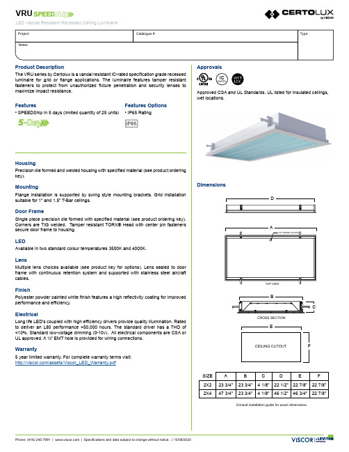
Consult installation guide for exact dimensions.CEILING CUTOUT SIZE A B C D E F 2X223 3/4”23 3/4” 4 1/8”22 1/2”22 7/8”22 7/8”2X447 3/4”23 3/4”4 1/8”46 1/2”46 3/4”22 7/8”ATOP VIEW7/8” WIRING ACCESSEDCROSS SECTIONCBFHousingPrecision die formed and welded housing with specified material (see product ordering key).MountingFlange installation is supported by swing style mounting brackets. Grid installation suitable for 1” and 1.5” T-Bar ceilings.Door FrameSingle piece precision die formed with specified material (see product ordering key). Corners are TIG welded. Tamper resistant TORX® Head with center pin fasteners secure door frame to housing.LEDAvailable in two standard colour temperatures 3500K and 4000K.LensMultiple lens choices available (see product key for options). Lens sealed to door frame with continuous retention system and supported with stainless steel aircraft cables.FinishPolyester powder painted white finish features a high reflectivity coating for improved performance and efficiency.ElectricalLong life LED’s coupled with high efficiency drivers provide quality illumination. Rated to deliver an L80 performance >50,000 hours. The standard driver has a THD of <10%. Standard low-voltage dimming (0-10v). All electrical components are CSA or UL approved. A ½” EMT hole is provided for wiring connections.Warranty5 year limited warranty. For complete warranty terms visit:/assets/Viscor_LED_Warranty.pdfDimensionsApprovalsApproved CSA and UL Standards. UL listed for insulated ceilings, wet locations.ICRATEDProduct DescriptionThe VRU series by Certolux is a vandal resistant IC-rated specification grade recessed luminaire for grid or flange applications. The luminaire features tamper resistant fasteners to protect from unauthorized fixture penetration and security lenses to maximize impact resistance.Features• SPEEDShip in 5 days (limited quantity of 25 units)Features Options• IP65 RatingOrder KeyEXAMPLE: VRUI2X2A/ALED840K055LUNV-P13/P45PhotometricCRI8 - (80-89)8A AVoltageUNV - 120-277V347 - 347VCCT35K - 3500 K40K - 4000 KSize NominalLumens Watts 2x25500532x45500477000611000082LEDVRUSeriesSize(Width xLength)2x22x4 Door StyleI - InsetO - OverlappingDoorGaugeA - 18 Ga. CRS - PaintedHousingGaugeA - 18 Ga. CRS - PaintedInternal/ExternalLensP13 - .125 Prismatic AcrylicP45 - .125 Clear Polycarbonate/-/NominalLumens055L - 5500lm070L - 7000lm100L - 10000lm2x42x2VRUI-2X2-LED840K055LUNV-P82P08IES File:VRUI-2X2-LED840K055LUNV-P82P08Lumens:5569Wattage:52Efficacy:1070°10°20°30°40°50°60°70°80°90200 cd 400 cd 600 cd 800 cd 1000 cd 1200 cd 1400 cd 1600 cd 1800 cd 2000 cd 2200 cd 2400 cdZonal Lumen SummaryZone Lumens%Lamp0.0° - 30.0°1723-43,083.6%30.9%0.0° - 40.0°2764-69,091.0%49.6%0.0° - 60.0°4646-116,155.7%83.4%0.0° - 90.0°5569-139,225.4%100.0%Average Luminance Table (cd/m2)CP Summary0.00°45.00°90.00°0.00°63646364636445.00°52025147523255.00°46644579468165.00°39103791391575.00°26592559278085.00°79711701738Coefficients of Utilizationρc80%70%50%ρw70%50%30%70%50%30%70%50%30%0119119119116116116111111111111010510110710399102999621009386989185938782392827489807385777148473658272647869625786557766456726255672595070585067564976754456553456251448624941614841584740958453757453754443610554234534134514033Effective Floor Cavity Reflectance: 20%P13P45OptionsApproval OptionsX8 IP65 RatingOther options may be available, consult factory.Specifications and data subject to change without notice.。
ENC28J60_cn中文手册

2
20
3
19
4 ENC28J60 18
5
17
6
16
7
15
8 9 1011121314
VDDOSC
OSC2 OSC1 VSSOSC VSSPLL VDDPLL VDDRX
2006 Microchip Technology Inc.
高级信息
DS39662A_CN 第 1 页
ENC28J60
目录
1.0 概述 ... 2.0 外部连接 ... 3.0 存储器构成 ... 4.0 串行外设接口 (SPI) ... 5.0 以太网概述 ... 6.0 初始化 ... 7.0 发送和接收数据包 ... 8.0 接收过滤器 ... 9.0 双工模式配置和协商 ... 10.0 流量控制 ... 11.0 复位 ... 12.0 中断 ... 13.0 直接存储器访问控制器 ... 14.0 掉电 ... 15.0 内置自测试控制器 ... 16.0 电气特性 ... 17.0 封装信息 ... 索引 ... 客户支持 ... 系统信息和升级热线 ... 读者反馈表 ... 产品标识体系 ...
... 3 .. 5 .. 11 . 25 .. 31 . 33 . 39 .. 47 ... 53 ... 55 . 59 . 65 .. 75 . 77 . 79 ... 83 ... 89 .. 95 . 97 . 97 ... 98 .. 99
致客户
我们旨在提供᳔佳文档供客户正确使用 Microchip 产品。为此,我们将不断改进出版物的内容和质量,使之更好地满足您的要求。 出版 物的质量将随新文档及更新版本的推出而得到提升。 如果您对本出版物有任何问题和建议,请通过电子邮件联系我公司 TRC 经理,电子邮件地址为 CTRC@,或将本 数据手册 后附的 《读者反馈表》传真到 86-21-5407 5066。我们期待您的反馈。
基于窄带 OFDM 载波和微功率无线双模通信技术 低压电力用户集中抄表系统运行及维护手册说明书

低压电力用户集中抄表系统运行及维护手册基于窄带载波和微功率无线双模通信技术低压电力用户集中抄表系统运行及维护手册北京博维亚讯技术有限公司版本:1.02016年5月20日北京博维亚讯技术有限公司地址:北京市昌平区回龙观镇北京国际信息产业基地发展路1号集智达大厦3层邮编:102206电话:传真:第 2 页 共29 页目录1文档说明 (4)1.1文档范围 (4)1.2文档目的 (5)1.3参考文献 (5)1.4术语和定义 (5)1.5缩写词 (6)2关于博维亚讯 (7)3低压电力用户集中抄表系统简介 (7)4博维亚讯双模方案介绍 (9)4.1双模方案简介 (9)4.2博维亚讯双模模块技术特点 (10)4.2.1窄带OFDM载波技术特点 (10)4.2.2微功率无线技术特点 (11)5博维亚讯双模产品介绍 (11)6产品安装及注意事项 (13)6.1注意事项 (13)6.2集中器安装 (13)6.2.1安装位置要求 (13)6.2.2集中器设备安装 (14)6.2.3天线安装 (15)6.3采集器安装说明 (17)6.4双模智能电表模块安装 (22)7产品运行 (22)8产品维护 (23)8.1故障现象 (24)8.2故障原因 (25)第 3 页共29 页8.3排查方法 (26)8.4解决方案 (29)1文档说明1.1文档范围本文档适用于电力企业基于力合窄带OFDM载波和微功率无线双模通信技术低压电力用户集中抄表系统安装、运行和维护人员。
第 4 页共29 页1.2文档目的本文档目的为电力企业基于力合窄带OFDM载波和微功率无线通信技术低压电力用户集中抄表系统安装、运行和维护人员在日常工作过程中提供帮助和指导。
1.3参考文献介于本文档参考文件过多,在这里不详细列出,具体请按照下列描述内容查阅相关标准文献。
①电力行业标准 DL/T645-2007多功能电能表通信协议②Q/CSG 11109003-2013《中国南方电网有限责任公司低压电力用户集中抄表系统集中器技术规范》③Q/CSG 11109005-2013《中国南网电网有限责任公司低压电力用户集中抄表系统采集器技术规范》④北京博维亚讯技术有限公司2014年低压电力线窄带OFDM载波和微功率无线双模通信产品企业标准1.4术语和定义计量自动化主站:计量自动化主站是指具有选择终端并与终端进行信息交换功能的计算机设备,包括前置采集、数据维护存储、业务处理和综合应用四个部分,其中前置采集部分完成和终端进行通讯的功能。
KYN28开关柜资料
1.概述KYN28-12型户内交流金属铠装移开式开关设备(以下简称开关柜),适用于3.6~12kV 三相交流50Hz电力系统,用于接受和分配电能并对电路实行控制、保护及监测。
符合标准:GB 3906-91 《3~35kV交流金属封闭开关设备》GB 11022-89 《高压开关设备通用技术条件》IEC 298(1990)《额定电压1kV以上、50kV及以下交流金属封闭开关设备和控制设备》DL 404-91 《户内交流高压开关柜订货技术条件》2.型号及含义K Y N 28 - 12 / □1-□2□3□4□5产品名称K 金属封闭铠装开关设备结构特征Y 移开式(手车式)使用条件N 户内使用设计序号28额定电压12 kV额定电流□1 A额定短路开断电流□2kA一次方案号□3操动方式□4D-电磁式,T-弹簧式环境特征□5TH-湿热带,TA-干热带,G-高海拔断路器种类Z-真空,S(或不标)-少油,F-SF63.使用环境条件3.1环境温度:最高温度+40℃,最低温度-10℃。
3.2环境湿度:日平均相对湿度≤95%,月平均相对湿度≤90%。
3.3海拔高度:1000m以下。
3.4抗地震度:地震烈度不超过8度。
3.5周围空气应不受腐蚀性或可燃性气体、水蒸汽等明显污染。
3.6无经常性的剧烈振动场所。
3.7在超过GB 3096-91规定的正常的环境条件下使用式,由用户和制造厂协商。
4.技术参数4.1 开关设备技术参数见表1。
4.2 VD4、VS1真空断路器技术参数4.2.1 VD4、VS1真空断路器技术参数见表2。
4.2.2 VD4、VS1真空断路器机械特性见表3。
4.3 操动机构技术参数见表4。
表2 VD4、VS1真空断路器技术参数表3 VD4、VS1真空断路器机械特性要求由用户与制造厂联系协商;当断路器用于开断电容器组时,电容器组的额定电流不应大于断路器额定电流的80%。
5.结构特点开关设备按GB 3906-91中的金属铠装移开式开关设备而设计。
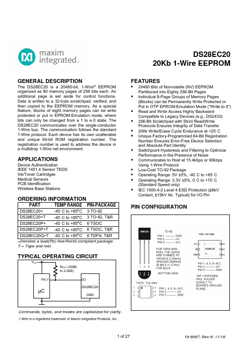
DS28EC20(MAXIM) 数据手册20KBIT TO92-3-qegoo
Stresses beyond those listed under “Absolute Maximum Ratings” may cause permanent damage to the device. These are stress ratings only, and functional operation of the device at these or any other conditions beyond those indicated in the operational sections of the specifications is not implied. Exposure to the absolute maximum rating conditions for extended periods may affect device reliability.
PIN CONFIGURATION
TYPICAL OPERATING CIRCUIT
VCC RPUP (300Ω to 2.2kΩ) PX.Y I/O DS28EC20
µC
GND
Commands, bytes, and modes are capitalized for clarity.
1-Wire is a registered trademark of Maxim Integrated Products, Inc.
5.0V SUPPLY ELECTRICAL CHARACTERISTICS
(VPUP = 5.0V ±5%, TA = -40°C to +85°C, unless otherwise noted.) (Note 1)
PARAMETER I/O PIN GENERAL DATA 1-Wire Pullup Resistance Input Capacitance Input Load Current High-to-Low Switching Threshold Input Low Voltage Low-to-High Switching Threshold Switching Hysteresis Output Low Voltage Recovery Time (Notes 2, 12) Rising-Edge Hold-off Time (Notes 5, 13) Timeslot Duration (Notes 2, 14) RPUP CIO IL VTL VIL VTH VHY VOL tREC tREH tSLOT (Notes 2, 3) (Notes 4, 5) I/O pin at VPUP (Notes 5, 6, 7) (Notes 2, 8) (Notes 5, 6, 9) (Notes 5, 6, 10) At 4mA (Note 11) Standard speed Overdrive speed Standard speed Overdrive speed Standard speed Overdrive speed Standard speed Overdrive speed Standard speed Overdrive speed Standard speed Overdrive speed Standard speed Overdrive speed Standard speed Overdrive speed Standard speed Overdrive speed Standard speed Overdrive speed Standard speed Overdrive speed 2.5 0.30 5 5 0.5 Not applicable (0) 65 11 480 48 15 2 60 8 60 6 60 6 1 1 5 0.800 tRL + δ tRL + δ 640 80 60 6 240 24 75 10 120 15.5 15 2 15 - δ 2-δ 15 2.27 0.3 2000 0.05 1.6 3.5 VPUP 1.8 0.5 VPUP 1.1 1.30 0.20 2.2 kΩ pF µA V V V V V µs 5.0 µs µs SYMBOL CONDITIONS MIN TYP MAX UNITS
vestas电气参数
等级: I编号:944761zh.R92007-04-13电气参数V66-1.75 MWV80-2.0 MWV90-1.8/2.0 MW1.75/1.8/2.0 MW-690V-50Hz-VMP5000控制器维斯塔斯风力系统公司中文技术文件仅供参考,以英文版为准电气参数目录 ……………………………………………………………………………..…………..页码1. 1.75/1.8/2.0 MW风机 (1)2.VMP控制器 (1)3.高压联网 (2)4.高压开关柜 (2)5.高压开关柜接地 (2)6.变压器 (3)7.风机接地系统/防雷击保护 (3)8.发电机额定参数 (4)8.1V66-1.75MW无功功率的控制图 (5)8.2V80-2.0MW/V90-2.0MW无功功率的控制图 (6)8.3V90-1.8MW无功功率的控制图 (7)9.机舱控制器的短路保护 (8)10.电网监视 (9)11.选项 (9)12.电气保护 (9)13.图纸 (9)1. 1.75/1.8/2.0 MW风机VESTAS 1.75/1.8/2.0 MW是变桨距风机,因而运行和停机时,叶片总能保持最佳角度。
发电机是带绕组转子、滑环和VESTAS变频系统(VCS)的特殊异步电机,可使风机以不同的速度进行运转。
变速、变桨风机的优点包括以下几点:z在各种风况下优化出力z出力限定为1.75/1.8/2.0 MWz平稳且高质量的功率输出及低闪络率z无需电动机协助起动z无需使用机械刹车来停机z机械传动系统中,使载荷波动最小z可提供不同等级的噪声排放水平2.VMP控制器采用VMP(Vestas多处理器)控制器,风机运行自动化,其具有以下功能:z为限制起动电流,联网前使发电机转速与电网频率同步;z切入电流低于额定电流;z机舱可依据风向自动偏航z按照第10小节–电网监视,监视电网运行数据z监视运行z故障情况下停机VMP控制器包括一个机舱控制器、一个轮毂控制器和一个地面控制器。