450nm50mw欧司朗蓝色激光器技术规格书
最新ED020侧发光蓝光灯珠规格书460-463.5nm
LED020侧发光蓝光规格书产品型号:YT-020B 蓝光适用于: 顺向电流 IF=20mA目录1.特性2.应用范围3.产品外观尺寸4.最大绝对标称值5.光电特性参数6.典型光电参数曲线7.编带规格8.包装方式9.BIN级范围10.可靠度实验项目及条件11.使用注意事项1、特性:1.1 封装尺寸:3.8x1.0x0.6mm1.2发光颜色:蓝色1.3胶体颜色:无色透明1.4焊接方式:回流焊1.5符合RoHS 标准2、应用范围:2.1手机按键2.2一般应用3、成品外观尺寸:备注:1.所有尺寸均以mm 为单位4、最大绝对标称值(环境温度=25℃):5.光电特性参数(环境温度=25℃):备注:1.亮度偏差:±5% 2.电压偏差:±0.033.主波长偏差:±16.典型光电参数曲线40IF(mA)IF(mA)80 604020Vf(V)0.020.0 40.0 60.0 80.0 Ta(°C)100.0 FIG.1 FORWARD CURRENT VS. FORWARD VOLTAGE.FIG.2 MAXIMUM FORWARD DC CURRENT VSAMBIENT TEMPERATURE(Tjmax=105 °C)Half PowerWL=150nmI (RELATIVE LUMINOUS INTENSITY)5.04.03.02.01.00.0 0.020.040.060.080.0If(mA) 100.0400600 FIG.3 RELATIVE LUMINOUS INTENSITY VS. FORWARD CURRENTFIG.4 RELATIVE LUMINOUS INTENSITY VS. WAVELENGTH.50% Power Angle:120°0°le(%)100%80%60%40%20%-90°-60°-30° 0 30° 60°0%90°FIG.5 FAR FIELD PATTERN7. 编带规格:(单位:mm )包装数量 1000-4000pcs/卷8.包装方式:(单位:mm)9.BIN 级范围正向电压VF(公差:±0.05V):20MA测试亮度IV(公差:±5%):10.可靠度实验项目及条件:可靠度实验不合格判定标准:IV:衰减超过 30%VF:变化超过 20%备注:1、同一项实验结果的测试需在 2 个小时之内完成;2、测试必须在每项实验完成后、材料恢复正常环境条件下才能进行.11.使用注意事项11.1焊接SMD LED 灌封胶较软,外力易损坏发光面及塑料壳,焊接时要轻拿轻放。
Kingbright 蓝色LED灯的数据手册说明书
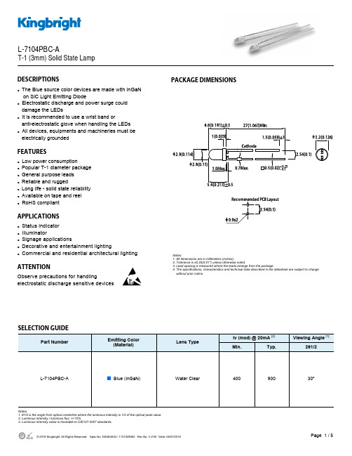
Part NumberEmitting Color (Material)Lens TypeIv (mcd) @ 20mA [2] Viewing Angle [1]Min. Typ. 2θ1/2L-7104PBC-A■ Blue (InGaN)Water Clear 400 30°900DESCRIPTIONSzThe Blue source color devices are made with InGaN on SiC Light Emitting Diodez Electrostatic discharge and power surge could damage the LEDsz It is recommended to use a wrist band oranti-electrostatic glove when handling the LEDs z All devices, equipments and machineries must be electrically groundedFEATURESzLow power consumptionz Popular T-1 diameter package z General purpose leads z Reliable and ruggedz Long life - solid state reliability z Available on tape and reel z RoHS compliantAPPLICATIONSz Status indicator z Illuminatorz Signage applicationsz Decorative and entertainment lightingzCommercial and residential architectural lightingATTENTIONObserve precautions for handlingelectrostatic discharge sensitive devicesPACKAGE DIMENSIONSL-7104PBC-AT-1 (3mm) Solid State LampSELECTION GUIDENotes:1. θ1/2 is the angle from optical centerline where the luminous intensity is 1/2 of the optical peak value.2. Luminous intensity / luminous flux: +/-15%.3. Luminous intensity value is traceable to CIE127-2007 standards.Notes:1. All dimensions are in millimeters (inches).2. Tolerance is ±0.25(0.01") unless otherwise noted.3. Lead spacing is measured where the leads emerge from the package.4. The specifications, characteristics and technical data described in the datasheet are subject to change without prior notice.ABSOLUTE MAXIMUM RATINGS at T A =25°CELECTRICAL / OPTICAL CHARACTERISTICS at T A =25°CNotes:1. 1/10 Duty Cycle, 0.1ms Pulse Width.2. 2mm below package base.3. 5mm below package base.4. Relative humidity levels maintained between 40% and 60% in production area are recommended to avoid the build-up of static electricity – Ref JEDEC/JESD625-A and JEDEC/J-STD-033.Notes:1. The dominant wavelength (λd) above is the setup value of the sorting machine. (Tolerance λd : ±1nm. )2. Forward voltage: ±0.1V.3. Wavelength value is traceable to CIE127-2007 standards.4. Excess driving current and / or operating temperature higher than recommended conditions may result in severe light degradation or premature failure.ParameterSymbol Value Unit Power Dissipation P D 120 mW Reverse Voltage V R 5 V Junction Temperature T j 125 °C Operating Temperature T op -40 to +85 °C Storage Temperature T stg -40 to +85°C DC Forward Current I F 30 mA Peak Forward CurrentI FM [1]100 mA Electrostatic Discharge Threshold (HBM) -1000VLead Solder Temperature [2] 260°C For 3 Seconds Lead Solder Temperature [3]260°C For 5 SecondsParameterSymbol Emitting ColorValue Unit Typ. Max. Wavelength at Peak Emission I F = 20mA λpeak Blue 468 - nm Dominant Wavelength I F = 20mA λdom [1] Blue 465 - nm Spectral Bandwidth at 50% Φ REL MAX I F = 20mA Δλ Blue 21 - nm CapacitanceC Blue 100 - pF Forward Voltage I F = 20mA V F [2] Blue 3.2 4 V Reverse Current (V R = 5V)I RBlue-10uATECHNICAL DATABLUERECOMMENDED WAVE SOLDERING PROFILENotes:1. Recommend pre-heat temperature of 105°C or less (as measured with a thermocoupleattached to the LED pins) prior to immersion in the solder wave with a maximum solder bath temperature of 260°C2. Peak wave soldering temperature between 245°C ~ 255°C for 3 sec (5 sec max).3. Do not apply stress to the epoxy resin while the temperature is above 85°C.4. Fixtures should not incur stress on the component when mounting and during soldering process.5. SAC 305 solder alloy is recommended.6. No more than one wave soldering pass.PACKING & LABEL SPECIFICATIONSPRECAUTIONSStorage conditions1. Avoid continued exposure to the condensing moisture environment and keep the product away from rapid transitions in ambient temperature.2. LEDs should be stored with temperature ≤ 30°C and relative humidity < 60%.3. Product in the original sealed package is recommended to be assembled within 72 hours of opening. Product in opened package for more than a week should be baked for 30 (+10/-0) hours at 85 ~ 100°C.2. When soldering wires to the LED, each wire joint should be separately insulated with heat-shrink tube to prevent short-circuit contact. Do not bundle both wires in one heat shrink tube to avoid pinching the LED leads. Pinching stress on the LED leads may damage the internal structures and cause failure.3. Use stand-offs (Fig.1) or spacers (Fig.2) to securely position the LED above the PCB.4. Maintain a minimum of 3mm clearance between the base of the LED lens and the first lead bend (Fig. 3 ,Fig. 4).5. During lead forming, use tools or jigs to hold the leads securely so that the bending force will not be transmitted to the LED lens and its internal structures. Do not perform lead forming once the component has been mounted onto the PCB. (Fig. 5 )LED Mounting Method1. The lead pitch of the LED must match the pitch of the mounting holes on the PCB during component placement.Lead-forming may be required to insure the lead pitch matches the hole pitch.Refer to the figure below for proper lead forming procedures.Note 1-3: Do not route PCB trace in the contact area between the leadframe and the PCB to prevent short-circuits." ○" Correct mounting method " x " Incorrect mounting methodLead Forming Procedures1. Do not bend the leads more than twice. (Fig. 6 )2. During soldering, component covers and holders should leaveclearance to avoid placing damaging stress on the LED duringsoldering.(Fig. 7)3. The tip of the soldering iron should never touch the lens epoxy.4. Through-hole LEDs are incompatible with reflow soldering.5. If the LED will undergo multiple soldering passes or face otherprocesses where the part may be subjected to intense heat,please check with Kingbright for compatibility.PRECAUTIONARY NOTES1. The information included in this document reflects representative usage scenarios and is intended for technical reference only.2. The part number, type, and specifications mentioned in this document are subject to future change and improvement without notice. Before production usage customer should refer tothe latest datasheet for the updated specifications.3. When using the products referenced in this document, please make sure the product is being operated within the environmental and electrical limits specified in the datasheet. Ifcustomer usage exceeds the specified limits, Kingbright will not be responsible for any subsequent issues.4. The information in this document applies to typical usage in consumer electronics applications. If customer's application has special reliability requirements or have life-threateningliabilities, such as automotive or medical usage, please consult with Kingbright representative for further assistance.5. The contents and information of this document may not be reproduced or re-transmitted without permission by Kingbright.6. All design applications should refer to Kingbright application notes available at /application_notes。
欧司朗LED规格书SFH 4050-850nm

High Power Infrared Emitter (850 nm)Version 1.7SFH 4050Ordering Information Features: •Very small package: (LxWxH) 1.7 mm x 0.8 mm x 0.65 mm •Short switching times •High optical total power Applications•Miniature photointerrupters •Industrial electronics •For control and drive circuits •Sensor technology •Alarm and safety equipment •Not for new designs in automotive applications NotesDepending on the mode of operation, these devices emit highly concentrated non visible infrared light which can be hazardous to the human eye. Products which incorporate these devices have to follow the safety precautions given in IEC 60825-1 and IEC 62471.Note:Measured at a solid angle of Ω = 0.01 srMaximum Ratings (T= 25 °C)Characteristics (TGrouping (T= 25 °C)Note:measured at a solid angle of Ω = 0.01 srOnly one group in one packing unit (variation lower 2:1).Relative Spectral Emission 3) page 12 I rel = f(λ), T A = 25°CRadiant Intensity 3) page 12I e / I e (100 mA) = f(I F ), single pulse, t p = 25 µs, T A = 25°C7000nm %OHF0413220406080100950750800850I λOHL0171510-3mA 101105510-1-2510e I I F1011021031055Max. Permissible Forward Current I F = f (T A ), RthJA = 450 K/WForward Current 3) page 12I F = f(V F ), single pulse, t p = 100 µs, T A = 25°CPermissible Pulse Handling CapabilityI F = f(t p ), T A = 25 °C, duty cycle D = parameterPermissible Pulse Handling CapabilityI F = f(t p ), T A = 85 °C, duty cycle D = parameterOHR0088302040608010012020406080100120mA˚C AR thjA = 450 K/WOHL01713I 10-40.51 1.52 2.5V3100A0F-1105510-2-3510t pA I10101010101010s 2100.10.20.30.40.50.60.70.80.91.1t p0A I 10101010101010s 2100.10.20.30.40.50.60.70.81.0Radiation Characteristics 3) page 12 I rel = f(ϕ), T A = 25°CPackage OutlineDimensions in mm (inch).PackageSmartLED (EIA 0603), Epoxy, colourless, slightly diffused100˚90˚80˚70˚60˚50˚GPLY7036+0.05 (0.002)0.125 (0.005)-0.05 (0.002)0.65 (0.026)±0.1 (0.004)±0.05 (0.002)Approximate Weight:2.1 mgRecommended Solder PadDimensions in mm (inch).OHAPY606Alternative Solder PadDimensions in mm (inch).Reflow Soldering ProfileProduct complies to MSL Level 2 acc. to JEDEC J-STD-020D.01OHPY3832Copper solder pad50100150200250300t ˚CTapingDimensions in mm [inch].* slope calculation D T/D t: D t max. 5 s; fulfillment for the whole T-rangeTape dimensions [mm]Reel dimensions [mm]Barcode-Product-Label (BPL)Tape and Reel8 mm tape with 5000 pcs. on ∅ 180 mm reelOHA04563(G) GROUP:1234567890(1T) LOT NO:(X) PROD NO:123456789LX XXXXRoHS CompliantBIN1: XX-XX-X-XXX-XML X Temp STXXX °C XPack: RXX DEMYX_X123_1234.1234 X9999(Q)QTY: 4 X _1234.1234 X XX-X-X3_1234X-XX-X- RXX XXXX_X123_123XX-XX-X 234Pack: RX D) D/C:/C:(9D) D 567890NO:123456789torsH NO:123456uctors OptoE XAM PL E678901234(9D) D/C:(6P) BATCH NO:1234567890OSRAM Opto XX-XX-X-X SemiconductorsDry Packing Process and MaterialsNote:Moisture-sensitive product is packed in a dry bag containing desiccant and a humidity card.Regarding dry pack you will find further information in the internet. Here you will also find the normative references like JEDEC.Transportation Packing and MaterialsDimensions of transportation box in mmOHA00539Barcode labelDisclaimerLanguage english will prevail in case of any discrepancies or deviations between the two language wordings. Attention please!The information describes the type of component and shall not be considered as assured characteristics.Terms of delivery and rights to change design reserved. Due to technical requirements components may contain dangerous substances.For information on the types in question please contact our Sales Organization.If printed or downloaded, please find the latest version in the Internet.PackingPlease use the recycling operators known to you. We can also help you – get in touch with your nearest sales office. By agreement we will take packing material back, if it is sorted. You must bear the costs of transport. For packing material that is returned to us unsorted or which we are not obliged to accept, we shall have to invoice you for any costs incurred.Components used in life-support devices or systems must be expressly authorized for such purpose! Critical components* may only be used in life-support devices** or systems with the express written approval of OSRAM OS.*) A critical component is a component used in a life-support device or system whose failure can reasonably be expected to cause the failure of that life-support device or system, or to affect its safety or the effectiveness of that device or system.**) Life support devices or systems are intended (a) to be implanted in the human body, or (b) to support and/or maintain and sustain human life. If they fail, it is reasonable to assume that the health and the life of the user may be endangered.Glossary1)Thermal resistance: junction -ambient, mounted on PC-board (FR4), padsize 5 mm2 each2)Thermal resistance: junction - soldering point, of the device only, mounted on an ideal heatsink (e.g. metal block)3)Typical Values: Due to the special conditions of the manufacturing processes of LED, the typical data or calculated correlations of technical parameters can only reflect statistical figures. These do not necessarily correspond to the actual parameters of each single product, which could differ from the typical data and calculated correlations or the typical characteristic line. If requested, e.g. because of technical improvements, these typ. data will be changed without any further notice.Published by OSRAM Opto Semiconductors GmbHLeibnizstraße 4, D-93055 Regensburg © All Rights Reserved.。
445nm蓝光激光器一体说明书

蓝光激光器使用说明书为了更好的使用本产品,使用前请先认真阅读本说明书,并将其妥善保存,以备将来之用地址Add:北京市朝阳区酒仙桥东路1号,电子称科技园M7栋东4层电话Tel:(+86)-010-********一、产品描述1.1产品描述:产品名称为二极管泵浦全固体激光器(DPSSL),波长为445nm,输出功率可根据客户需要自主进行调节,功率输出范围是(0mW-500mW);交流电AC 输入范围是(90V-265V),具体操作可参照手册说明进行操作。
1.2产品特点及应用:镭志威生产的激光器与其他同种产品来说,优势是体积小、效率高、功率稳定性好、光斑质量好、运输和使用方便、无污染。
目前在工业和科研领域的应用已包括材料处理、医疗诊断、仪器制造、基础研究、光存储、娱乐、图像记录、检测与控制、全色显示、测向与指示、国防军事等。
1.3安全注意1.3.1激光对人体和眼睛具有潜在危害,严禁用激光照射他人,尤其眼睛。
1.3.2不可将激光长时间照射到人体或易燃物体,以免因激光发热引起事故。
1.3.3调试过程中应在激光输出的光路上放置一块吸收性能良好的黑色金属材料作为光束终止器,防止引起火灾事故。
1.3.3工作场所无反射物(玻璃\镜子及金属物)并保证使激光射向安全的地方,所有现场人员佩戴激光防护眼镜。
1.3.4工作中的激光装置,假如不发出激光,也不要用眼睛探视光路。
1.4使用环境及要求1.4.1本产品应在干燥、清洁和无静电环境中使用,工作环境温度10~35℃,适宜工作环境温度20~30℃,避免高温、高湿和剧烈震动、冲击。
1.4.2必须保证激光头外壳温度与适宜工作温度相近后,才允许开启激光器,以免温差过大,影响激光器性能或损坏器件。
1.4.3搬动仪器时,请保持电源和激光头为一整体,不可提其中之一,而让另一部分处悬空状态。
警告:本产品属于4类激光设备,直接的强激光照射可以对人体皮肤产生严重伤害,特别是将使眼睛致盲,调试操作人员必须具备激光安全防护的常识,工作中必须佩戴针对445nm 波长的专用激光防护眼镜。
朗伯型大功率 LED 光源(光色均匀无黄圈)

4
-2.0
15
注意: (1)电压允许误差: ±0.1V (2)动态电阻是指 V-I 曲线线性区域斜率的倒数
典型光电特性曲线
2
朗伯型大功率 LED 光源(光色均匀无黄圈) A07/XXXX1-XX-F
典型光强分布图
3
朗伯型大功率 LED 光源(光色均匀无黄圈) A07/XXXX1-XX-F
典型光衰曲线
电气特性 (IF=350mA,T Ambient=25ºC)
颜色
正向电压 VF (V)
最小值
典型值
最大值
动态电阻 (Ω)RD
正向电压温度系数 热阻 (芯片与散热 (mV/ºC) ΔVF/ΔTJ 铜柱)(ºC/W)RVJ-C
白
2.7
------
3.6
1.5
-2.0
15
暖白
2.7
------
3.6
1.5
1
0.9
Relative Luminous Flux
0.8 50ºC
0.7
70ºC
0.6
90ºC
0.5
0.4
0.3 0
1000 2000 3000 4000 5000 6000 7000 8000 9000 10000 Time(hour)
注意:图中温度指 LED 底部散热铜柱温度
外形图
注意: (1) 单位(mm) (2)未注尺寸公差:±0.3mm
125 Class1
500 700
5 5 180
单位
摄氏度(ºC) 摄氏度(ºC) 摄氏度(ºC)
等级 毫安(mA) 毫安(mA) 伏特(V)
秒(S) 摄氏度(ºC)
1
欧司朗LED产品介绍

电压 正常工作功耗
正常光强 (启动10 分钟之后)
保护 等 级
接
线
OS-WL01AA1 红色
10
OS-WL01AY1 黄色
10
OS-WL01AV1
翠绿色
10
OS-WL01AB1 蓝色
10
24 VDC; 1.1 W
24 VDC; 1.1 W
24 VDC; 1.3 W
24 VDC; 1.3 W
3500
2500
• 低功率 ( < 10W/m)
• 低热量 • 长寿命 • 颜色可变 (任意选择)
制造商: Public screen Freigericht/Altenmittlau/D
制造商: Ilti/Italy
LINEARlight进行建筑照明
案例
Parkgate, Schwabing 德国 2002
建筑照明
COINlight 用于室外标志性照明或装饰性照明
案例
室外灯具 意大利 方向照明/效果照明 采用 COINlight 颜色: 蓝,白
COINlight 的装饰效果
案例
水晶灯 德国
效果照明 采用 COINlight 颜色: 蓝,红,白, 黄,绿
COINlight 型号综述
模块型号 可选颜色 LED数目 / 模块
光束方向 电源电压 正常功耗
保护等级
接
线
OS-CM01E-X -A,-Y,-T,-B, W
9
顶部发光
24 VDC; 1-1,2 W 由颜色决定
OS-CM01B-X -A,-Y,-T,-B, W
8
侧面发光
24 VDC; 0,5-0,9 W 由颜色决定
欧司朗LED规格书SFH 4248-950nm

High Power Infrared Emitter (940 nm)Version 1.4/ OS-IN-2015-033SFH 4248Ordering Information Features: •High Power Infrared LED •Short switching times •Half angle: ± 15°•High forward current allowed at high temperature •The product qualification test plan is based on the guidelines of AEC-Q101-REV-C, Stress Test Qualification for Automotive Grade Discrete Semiconductors.Applications •Infrared Illumination for cameras •IR data transmission •Sensor technology NotesDepending on the mode of operation, these devices emit highly concentrated non visible infrared light which can be hazardous to the human eye. Products which incorporate these devices have to follow the safety precautions given in IEC 60825-1 and IEC 62471.Note:Measured at a solid angle of Ω = 0.01 srMaximum Ratings (T= 25 °C)Characteristics (TGrouping (T= 25 °C)Note:measured at a solid angle of Ω = 0.01 srOnly one group in one packing unit (variation lower 2:1).Relative Spectral Emission 3) page 12 I rel = f(λ), T A = 25°CRadiant Intensity 3) page 12I e / I e (100 mA) = f(I F ), single pulse, t p = 25 µs, T A = 25°C8000nm %OHF0413420406080100I λ8509009501025OHF0382110-3mA 101105510-1-2510e e I I F1011021031055(100 mA)Max. Permissible Forward Current I F, max = f(T A ), R thJA = 300 K / WForward Current 3) page 12I F = f(V F ), single pulse, t p = 100 µs, T A = 25°CPermissible Pulse Handling CapabilityI F = f(t p ), T A = 25 °C, duty cycle D = parameterPermissible Pulse Handling CapabilityI F = f(t p ), T A = 85 °C, duty cycle D = parameter00˚C T I mAOHL01716A2040608010012020406080120OHF03822I 10-4V 100A0F-1105510-2-35100.51 1.52 2.521010101010t p1010s 100A I 0.20.40.60.81.01.2t pA I 10101010101010s 2100.10.20.30.40.50.60.70.80.91.1Radiation Characteristics 3) page 12 I rel = f(ϕ)Package OutlineDimensions in mm (inch).OHL0002150˚60˚70˚80˚90˚100˚GPLY6127PinningPackagePower TOPLED with Lens Approximate Weight:37 mgRecommended Solder PadDimensions in mm.Reflow Soldering ProfileProduct complies to MSL Level 2 acc. to JEDEC J-STD-020D.01050100150200250300tT ˚CAll temperatures refer to the center of the package, measured on the top of the component * slope calculation D T/D t: D t max. 5 s; fulfillment for the whole T-rangeTapingDimensions in mm. Tape and Reel12 mm tape with 2000 pcs. on ∅ 180 mm reelTape dimensions [mm]Reel dimensions [mm]Barcode-Product-Label (BPL)Dry Packing Process and MaterialsNote:Moisture-sensitive product is packed in a dry bag containing desiccant and a humidity card.Regarding dry pack you will find further information in the internet. Here you will also find the normative references like JEDEC.OHA04563(G) GROUP:1234567890(1T) LOT NO:(X) PROD NO:123456789LX XXXXRoHS CompliantBIN1: XX-XX-X-XXX-XML X Temp STXXX °C XPack: RXX DEMYX_X123_1234.1234 X 9999(Q)QTY: 4 X_1234.1234 X XX-X-X3_1234X-XX-X- RXX XXXX_X123_123XX-XX-X 234Pack: RX D) D/C:/C:(9D) D 567890NO:123456789torsH NO:123456uctors OptoE XAM PL E678901234(9D) D/C:(6P) BATCH NO:1234567890OSRAM Opto XX-XX-X-X Semiconductors OHA00539Barcode labelTransportation Packing and MaterialsDimensions of transportation box in mmDisclaimerLanguage english will prevail in case of any discrepancies or deviations between the two language wordings. Attention please!The information describes the type of component and shall not be considered as assured characteristics.Terms of delivery and rights to change design reserved. Due to technical requirements components may contain dangerous substances.For information on the types in question please contact our Sales Organization.If printed or downloaded, please find the latest version in the Internet.PackingPlease use the recycling operators known to you. We can also help you – get in touch with your nearest sales office. By agreement we will take packing material back, if it is sorted. You must bear the costs of transport. For packing material that is returned to us unsorted or which we are not obliged to accept, we shall have to invoice you for any costs incurred.Components used in life-support devices or systems must be expressly authorized for such purpose! Critical components* may only be used in life-support devices** or systems with the express written approval of OSRAM OS.*) A critical component is a component used in a life-support device or system whose failure can reasonably be expected to cause the failure of that life-support device or system, or to affect its safety or the effectiveness of that device or system.**) Life support devices or systems are intended (a) to be implanted in the human body, or (b) to support and/or maintain and sustain human life. If they fail, it is reasonable to assume that the health and the life of the user may be endangered.Glossary1)Thermal resistance: junction -ambient, mounted on PC-board (FR4), padsize 16 mm2 each2)Thermal resistance: junction - soldering point, of the device only, mounted on an ideal heatsink (e.g. metal block)3)Typical Values: Due to the special conditions of the manufacturing processes of LED, the typical data or calculated correlations of technical parameters can only reflect statistical figures. These do not necessarily correspond to the actual parameters of each single product, which could differ from the typical data and calculated correlations or the typical characteristic line. If requested, e.g. because of technical improvements, these typ. data will be changed without any further notice.Published by OSRAM Opto Semiconductors GmbHLeibnizstraße 4, D-93055 Regensburg © All Rights Reserved.。
欧司朗LED规格书
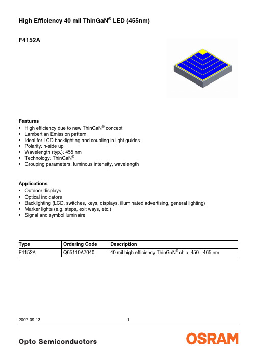
F4152AHigh Efficiency 40 mil ThinGaN ®LED (455nm)2007-09-131Features •High efficiency due to new ThinGaN ® concept •Lambertian Emission pattern•Ideal for LCD backlighting and coupling in light guides •Polarity: n-side up•Wavelength (typ.): 455 nm •Technology: ThinGaN ®•Grouping parameters: luminous intensity, wavelengthApplications •Outdoor displays •Optical indicators•Backlighting (LCD, switches, keys, displays, illuminated advertising, general lighting)•Marker lights (e.g. steps, exit ways, etc.)•Signal and symbol luminaireType Ordering Code DescriptionF4152AQ65110A704040 mil high efficiency ThinGaN ® chip, 450 - 465 nmElectrical values1)(T A = 25 °C)Parameter Symbol Value2)Unitmin.typ.max. Dominant wavelengthI F = 350 mA, pulsedλdom450465nm Reverse voltageI R = 10µAV R10VForward voltageI F = 350 mA, pulsed VF2.73.8VRadiant PowerI F = 350 mA, pulsedΙV32 a.u.1)Measurement limits describe actual settings and do not include measurement uncertainties. Each wafer and fragmentof a wafer is subject to final testing. The wafer or its pieces are individually attached on foils (rings). All el. values are referenced to the vendor's measurement system (correlation to customer product(s) is required). Measurement uncertainty +/-15% for brightness, +/- 1nm for wavelength and +/- 0.1V for voltage.2)Due to the special conditions of the manufacturing processes of LED, the typical data or calculated correlations oftechnical parameters can only reflect statistical figures. These do not necessarily correspond to the actual parameters of each single product, which could differ from the typical data and calculated correlations or the typical characteristic line. If requested, e.g. because of technical improvements, these typ. data will be changed without any further notice.2007-09-1322007-09-133Binning Maximum Ratings 1)Radiant Power 450 - 455 nm455 - 460 nm460 - 465 nm28.0 - 35.2 a.u.A1B1C135.2 - 41.2 a.u.A2B2C241.2 - 48.4 a.u.A3B3C348.4 - 56.8 a.u.A4B4C4> 56.8 a.u.A5B5C5ParameterSymbol Value Unit Maximum Operating temperature range T op -40...+100°C Maximum forward current (T A = 25°C)I F 700mA Minimum forward current (T A = 25°C)I F100mA Maximum surge Current (T A = 25°C)t p = 10 µs, D = 0.05I peak0.7A Maximum junction temperatureT j125°C1)Maximum ratings are strongly package dependent and may differ between different packages. The values given represent the chip in an OSRAM Opto Semiconductor’s Platinum Dragon® package.Mechanical values1)Parameter Symbol Value2)Unitmin.typ.max.Length of chip edge (x-direction)L x0.95 1.00 1.05mm Length of chip edge (y-direction)L y0.95 1.00 1.05mm Diameter of the wafer D50.8mmDie height H170190210µm Diameter of bondpad d130150170µm Additional informationMetallization frontside Gold partialMetallization backside AuDie bonding Epoxy bonding1)All chips are checked according to the following procedure and the OSRAM OS specification of the visual inspectionA63501-Q0013-N001-*-76G3:Unless otherwise described below, the quality level of the final visual inspection shall comply to an AQL 0,4 (according MIL-STD-105D, level II), if the customer performes an incoming visual inspection of a shipment. The quality inspection (final visual inspection) is performed by production. An additional visual inspection step as special release procedure by QM after the final visual inspection is not installed.2)Due to the special conditions of the manufacturing processes of LED, the typical data or calculated correlations oftechnical parameters can only reflect statistical figures. These do not necessarily correspond to the actual parameters of each single product, which could differ from the typical data and calculated correlations or the typical characteristic line. If requested, e.g. because of technical improvements, these typ. data will be changed without any further notice2007-09-1342007-09-135Chip OutlinesDimensions are specified as typicalvalues as follows: mm (inch).Published by OSRAM Opto Semiconductors GmbH Wernerwerkstrasse 2, D-93049 Regensburg © All Rights Reserved.Attention please!The information generally describes the type of component and shall not be considered as assured characteristics or detailed specification.Terms of delivery and rights to change design reserved. Due to technical requirements components may contain dangerous substances. For information on the types in question please contact our sales organization.Handling and Storage Conditions:Storage time for wafers in sealed condition shall not exceed 6 months (storage ambient conditions: Ta=15...30°C;relative humidity: < 60%).The hermetically sealed shipment lot shall be opened under temperature and moisture controlled cleanroom environment only. Customer has to follow the according rules for disposition of material that can be hazardous for humans and environment. Dice have to be handled ESD sensitive.PackingChips are placed on a blue foil with minimum size of 18 x 18 cm².For shipment the wafers of a shipment lot are arranged to stacks. The stack is put in a plastic ESD bag with a maximum of 14 wafers in one bag. A maximum of 4 bags is put in a packaging box. A maximum of 5 packaging boxes is put in a shipping carton which is sealed for storage and shipment.Please use the recycling operators known to you. We can also help you – get in touch with your nearest sales office. By agreement we will take packing material back, if it is sorted. You will have to bear the costs of transport. For packing material that is returned to us unsorted or which we are not obliged to accept, we shall have to invoice you for any costs incurred.Label and shipping documentsEach wafer is identified with a sticker, which is attached to each wafer. The label shows chip type, wafer number, quantity, binning and the minimum, average and maximum values of voltage, luminous intensity and wavelength. Each wafer shipment includes an additional document, which summarizes the content.Design objectives a) workabilityThe chip design was developed and released based on the the vendor’s standard assembly procedures and packaging. Bond strength properties are in accordance to MIL_STD-750D, method 2037. Whether the chip fits to the customer’s product(c) with its according die and wire bond procedures and packaging must be evaluated by the customer himself. If workability problems arise after this release a mutually conducted problem solving procedure has to be set up, if thechips are suspected of contributing to the problemsb) chip characteristicsThe chips are produced by the vendor with best effort, but on chip level a subset of the chip characteristics can be determined only. Performance of the chip in the customer’s product(s) can only be determined by the customer himself. Returns/ComplaintsTo return material because of technical or logistical reasons a RMA-number is necessary. Samples for analysis purposes can be send to OSRAM OS without credit.Shipping Conditions:If not otherwise arranged, the “General Conditions for the supply of products and services of the electrical and electronics industry” apply for any shipment. If these documents are not familiar to you, please request them at our nearest sales office.Components used in life-support devices or systems must be expressly authorized by us for such purpose! Critical components2), may only be used in life-support devices or systems3) with the express written approval of OSRAM OS.1) Typical (refered to as typ.) data are defined as long-term production mean values and are only given for information. This is not a specified value.2)A critical component is a component used in a life-support device or system whose failure can reasonably be expected to cause the failure of that life-support device or system, or to affect its safety or effectiveness of that device or system.3)Life support devices or systems are intended (a) to be implanted in the human body, or (b) to support and/or maintain and sustain human life. If they fail, it is reasonable to assume that the health of the user may be endangered.2007-09-136。