反激式开关电源外文翻译
反激式开关电源原理
与你分享(反激式开关电源原理)反激式开关电源是指使用反激高频变压器隔离输入输出回路的开关电源."反激"(FL Y BACK)的具体所指是当输入为高电平(开关管接通)时输出线路中串联的电感为放电状态,相反当输入为高电平(开关管断开)时输出线路中的串联的电感为充电状态.与之相对的是"正激"(FORWARD)式开关电源,当输入为高电平(开关管接通)时输出线路中串联的电感为充电状态,相反当输入为高电平(开关管断开)时输出线路中的串联的电感为放电状态,以此驱动负载.三相电机的配导线:(电机一个千瓦大约在2A)"1.5加二,2.5加三""4后加四,6后加六""25后加五,50后递增减五""百二导线,配百数" 该口诀是按三相380V交流电动机容量直接选配导线的。
"1.5加二"表示1.5mm2的铜芯塑料线,能配3.5kW的及以下的电动机。
由于4kW 电动机接近3.5kW的选取用范围,而且该口诀又有一定的余量,所以在速查表中4kW以下的电动机所选导线皆取1.5mm2。
"2.5加三"、"4后加四",表示2.5mm2及4mm2的铜芯塑料线分别能配5.5kW、8kW电动机。
"6后加六",是说从6mm2的开始,能配"加大六"kW的电动机。
即6mm2的可配12kW,选相近规格即配1lkW电动机。
10mm2可配16kW,选相近规格即配15kW电动机。
16mm2可配22kW电动机。
这中间还有18.5kW电动机,亦选16mm2的铜芯塑料线。
"25后加五",是说从25mm2开始,加数由六改为五了。
即25mm2可配30kW的电动机。
35mm2可配40kW,选相近规格即配37kW电动机。
"50后递增减五",是说从50mm2开始,由加大变成减少了,而且是逐级递增减五的。
反激开关电源

1,反激电路是由buck-boost拓扑演变而来,先分析一下buck-boost电路的工作过程。
工作时序说明:t0时刻,Q1开通,那么D1承受反向电压截止,电感电流在输入电压作用下线性上升。
t1时刻,Q1关断,由于电感电流不能突变,所以,电感电流通过D1,向C1充电。
并在C1两端电压作用下,电流下降。
t2时刻,Q1开通,开始一个新的周期。
从上面的波形图中,我们可以看到,在整个工作周期中,电感L1的电流都没有到零。
所以,这个工作模式是电流连续的CCM模式,又叫做能量不完全转移模式。
因为电感中的储能没有完全释放。
从工作过程我们也可以知道,这个拓扑能量传递的方式是,在MOS管开通时,向电感中储存能量,MOS管关断时,电感向输出电容释放能量。
MOS管不直接向负载传递能量。
整个能量传递过程是先储存再释放的过程。
整个电路的输出能力,取决于电感的储存能力。
我们还要注意到,根据电流流动的方向,可以判断出,在输入输出共地的情况下,输出的电压是负电压。
MOS管开通时,电感L1承受的是输入电压,MOS关断时,电感L1承受的是输出电压。
那么,在稳态时,电路要保证电感不进入饱和,必定要保证电感承受的正向和反向的伏秒积的平衡。
那么:Vin×(t1-t0)=Vout×(t2-t1),假如整个工作周期为T,占空比为D,那么就是:Vin×D=V out×(1-D)那么输出电压和占空比的关系就是:V out=Vin×D/(1-D)同时,我们注意看MOS管和二极管D1的电压应力,都是Vin+V out另外,因为是CCM模式,所以从电流波形上可以看出来,二极管存在反向恢复问题。
MOS开通时有电流尖峰。
上面的工作模式是电流连续的CCM模式。
在原图的基础上,把电感量降低为80uH,其他参数不变,仿真看稳态的波形如下:t0时刻,Q1开通,那么D1承受反向电压截止,电感电流在输入电压作用下从0开始线性上升。
开关电源需掌握的基本英语词汇
Reservoir(储能的)
Ripple current(纹波电流)
Self-heating(自加热)
Tantalum(钽)
Temperature coefficient(温度系数)
Capacitor definition(电容定义)
Charge pump(电荷泵)
Clamp circuit(钳位电路)
Compensation(补偿)
Control equation(控制等式)
Buck converter (Buck 变换器)
Compensation(补偿)
Control equation(控制等式)
Buck-Boost converter(Buck-Boost 变换器)
Ultra-fast(超快速)
Discontinuous operation(断续工作)
Dissipation factor(损耗因数)
E
Eddy current(涡流)
Electromagnetic compatibility(EMC,电磁兼容)
Electromagnetic interference(EMI,电磁干扰)
Universal input(通用输入)
V
Voltage doubler(电压倍增器)
Voltage mode PWM controller(电压模式PWM 控制器)
W
Wire table(导线一览表)
Z
Zener diode(齐纳二极管)
开关电源需掌握的基本英语词汇
A
Auxiliary supply(辅助电源)
B
B-H curve(磁化曲线)
电源拓扑结构介绍----正激和反激
变换器的介绍: Transformer introduction
变压器:原边(原级)primary side 和
副边(次级)secondary side 原边电感(励磁电感)--magnetizing inductance
漏感---leakage inductance
副边开路或者短路测量原边电感分别得励磁电感和漏感 变压器的作用:1. 电气隔离; 2. 变比不同,达到电压升降; 3. 磁耦合传送能量;
压器储存能量,磁通量增加。在导通期间,磁通的增加量
为:
( )
V in W1
* D * Ts
此过程中,副边绕组的电压为Vin/N(N为原边和副 边匝数比),整流二极管D3导通,给电感、电容充电和负
载供电。
2012-10-31
15
(2) MOS管截止时,变压器原边励磁电感中的电流不
能跃变(方向不变,大小连续变化),通过二极管D1和D2
式中,K13=W1/W3是原边与复位绕组的匝比,
K23=W2/W3 是副边与复位绕组的匝比。
2012-10-31
8
此时,整流二极管D1 关断,滤波电感电流iL1通过续
流二极管D2续流,与buck变换器类似。
在此开关模态中,加在Q上的电压VQ为:
VQ=Vin+K13*Vin。
电源电压Vin反向加在复位绕组W3上,故铁芯去磁, 铁芯磁通Ø减小: W3*dØ/dt=-Vin 铁芯磁通Ø的减小量为:Vin/W3*ΔD*Ts。
2. 和Boost、Buck变换器一样,Flyback变换器也 有电流连续和断续两种工作方式。对Flyback变换器
来说,电流连续是指变压器两个绕组的合成安匝在一 个开关周期中不为零,而电流断续是指合成安匝在Q 截止期间有一段时间为零。图中a、b、c 给出了变换 器在不同开关模态下的等效电路图。
开关电源03、flyback-converter

在电源电压 一定时开关管的电压和占空比有关, 故必须限制D 值。 二极管 D1承受的电压为
V D1 V0 V in K
反激变换器
开关电源技术—— tqzheng@
5
负载电流I0就是流过D1的电流平均值,由波形图可得 根据变压器的工作原理,有下面两个表达式:
W 1 I p min W 2 I s min
I s max
V0 L2
(1 D y )T s
在此过程中,磁芯中的磁通也线性减小,由
反激变换器
d
V0 W2
dt
磁通增量
(- )
V0 W2
(1 D y )T s
开关电源技术—— tqzheng@
4
四、基本关系 稳态工作时,Q导通时铁芯磁通 的增长量必等于Q关断时的减少量, ( )
p
in
dt
L1
t=Ton时ip达到最大值
I P max I P min
V in D y L1
Ts
在此过程中,磁芯中的磁通也线性增加 ,由
d
V in W1
dt
磁通增量
()
V in W1
D yTs
反激变换器
开关电源技术—— tqzheng@
3
三、开关Q关断工况
Fly-back Converter
反激变换器
开关电源技术—— tqzheng@
1
Flyback converter (反激变换器)
一、基本电路 由buck-boost推演而得. Iin Vin
隔离变压器
IP UP
IS D US
Iout Cf 率高; 2.输出电压纹波较大; 3.处理功率在150W以下; 4.小功率多组输出特别有效;
反激式开关电源工作原理
反激式开关电源工作原理反激式开关电源(Switch Mode Power Supply,简称SMPS)是指利用开关导通和反激耦合发挥效果的电源。
主要组成部件有金属氧化物半导体开关功率晶体管(MOSFET),反激变压器、铁心变压器、元件电容等,临界换流变压器的核心在于MOSFET的开关功率管,它的本质是一个继电器,即磁性调压变压器和开关放大器的内部集成产物。
反激式开关电源的工作原理是:变压器的终端依靠MOSFET的开关功率管以脉冲宽度调制的方式进行以比经变压器不管它工作的频率转换,以进行检测变压器的输出电压,综合电路将信号反馈输入MOSFET,形成闭环控制。
MOSFET的开关功率管控制器经过控制,使原有拓扑结构变为变压器输出电压要求的额定输出电压值。
开关导通由MOSFET放大器控制,即PWM模块。
它调节MOSFET的开通频率和占空比,使其能按需要的频率、效率和相应的电压输出,电流以金属氧化物半导体开关功率晶体管的开启和关闭来实现,将输入高频调制脉冲输出到变压器的一转绕组,此处的传感依赖与金属氧化物半导体管,微处理器监测变压器的二转绕组的质量,当质量达到设定的电压值时,信号告诉PWM模块关闭MOSFET,以调节输出电压,既起到调节和控制变压器的输出电压作用。
反激开关电源上配有反激变压器,其终端可由MOSFET的开关导通而输出脉冲变化的PWM脉冲,使反激变压器的过热和短路保护功能得以激活,从而保证反激、铁心变压器更加安全可靠地工作。
反激开关电源上配有铁心变压器,其功能是在变压器漏感、双极管和滤波电容之间形成一个特殊的电路,以稳定变压器输出纹波,使输出电压得到优化,补偿电容部件能够补偿发生在反激变压器和铁心变压器之间的变化。
另外,随着SMPS在电源的应用的不断深入,电源的效率、稳定性和可靠性也大大提高。
由于反激开关电源的几个优势在技术性、成本性和简便性等方面,反激开关电源越来越受到重视,在电源领域得到更广泛的应用。
开关电源专业电子中英文词汇
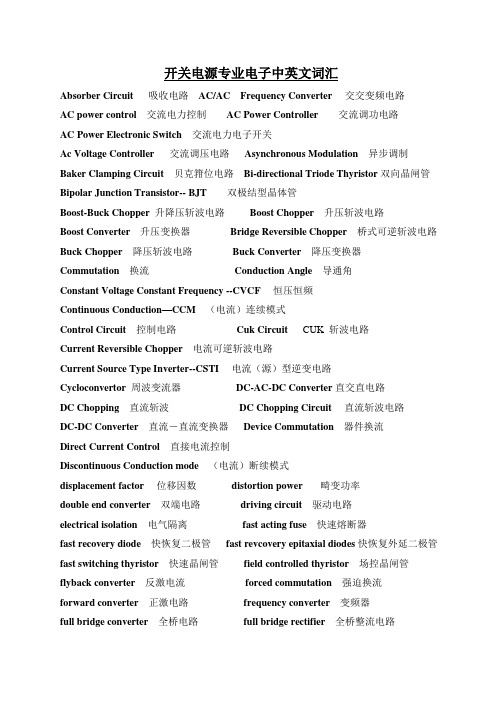
开关电源专业电子中英文词汇Absorber Circuit 吸收电路AC/AC Frequency Converter 交交变频电路AC power control交流电力控制AC Power Controller交流调功电路AC Power Electronic Switch交流电力电子开关Ac Voltage Controller交流调压电路Asynchronous Modulation异步调制Baker Clamping Circuit 贝克箝位电路Bi-directional Triode Thyristor双向晶闸管Bipolar Junction Transistor-- BJT双极结型晶体管Boost-Buck Chopper 升降压斩波电路Boost Chopper 升压斩波电路Boost Converter 升压变换器Bridge Reversible Chopper 桥式可逆斩波电路Buck Chopper 降压斩波电路Buck Converter 降压变换器Commutation 换流Conduction Angle 导通角Constant Voltage Constant Frequency --CVCF 恒压恒频Continuous Conduction—CCM (电流)连续模式Control Circuit 控制电路Cuk Circuit CUK 斩波电路Current Reversible Chopper 电流可逆斩波电路Current Source Type Inverter--CSTI 电流(源)型逆变电路Cycloconvertor 周波变流器DC-AC-DC Converter直交直电路DC Chopping 直流斩波DC Chopping Circuit 直流斩波电路DC-DC Converter 直流-直流变换器Device Commutation 器件换流Direct Current Control 直接电流控制Discontinuous Conduction mode (电流)断续模式displacement factor 位移因数distortion power 畸变功率double end converter 双端电路driving circuit 驱动电路electrical isolation 电气隔离fast acting fuse 快速熔断器fast recovery diode 快恢复二极管fast revcovery epitaxial diodes快恢复外延二极管fast switching thyristor 快速晶闸管field controlled thyristor 场控晶闸管flyback converter 反激电流forced commutation 强迫换流forward converter 正激电路frequency converter 变频器full bridge converter 全桥电路full bridge rectifier 全桥整流电路full wave rectifier 全波整流电路fundamental factor 基波因数gate turn-off thyristor——GTO可关断晶闸管general purpose diode普通二极管giant transistor——GTR电力晶体管half bridge converter 半桥电路hard switching 硬开关high voltage IC 高压集成电路hysteresis comparison 带环比较方式indirect current control 间接电流控制indirect DC-DC converter 直接电流变换电路insulated-gate bipolar transistor-----IGBT绝缘栅双极晶体管intelligent power module-------IPM智能功率模块integrated gate-commutated thyristor------IGCT集成门极换流晶闸管inversion 逆变latching effect 擎住效应leakage inductance 漏感light triggered thyristo---LTT光控晶闸管line commutation 电网换流load commutation 负载换流loop current 环流Schottky Barrier Diode 肖特基二极管。
开关电源外文文献翻译

开关电源外文文献翻译(文档含中英文对照即英文原文和中文翻译)外文:Switched-mode power supplyA switched-mode power supply (also switching-mode power supply, SMPS, or simply switcher) is an electronic power supply unit (PSU) that incorporates a switching regulator. While a linear regulator maintains the desired output voltage by dissipating excess power in a pass power transistor, the switched-mode power supply switches a power transistor between saturation (full on) and cutoff (completely off) with a variable duty cycle whose average is the desired output voltage. It switches at a much-higher frequency (tens to hundreds of kHz) than that of the AC line (mains), which means that the transformer that it feeds can be much smaller than one connected directly to the line/mains. Switching creates a rectangular waveform that typically goes to the primary of the transformer; typically several secondaries feed rectifiers, series inductors, and filter capacitors to provide various DC outputs with low ripple.The main advantage of this method is greater efficiency because the switching transistor dissipates little power in the saturated state and the off state compared to the semiconducting state (active region). Other advantages include smaller size and lighter weight (from the elimination of low frequency transformers which have a high weight) and lower heat generation due to higher efficiency. Disadvantages include greater complexity, the generation of high amplitude, high frequency energy that the low-pass filter must block to avoid electromagnetic interference (EMI), and a ripple voltage at the switching frequency and the harmonic frequencies thereof.A note about terminologyAlthough the term "power supply" has been in use since radios were first powered from the line/mains, that does not mean that it is a source of power, in the sense that a battery provides power. It is simply a device that (usually) accepts commercial AC power and provides one or more DC outputs. It would be more correctly referred to as a power converter, but long usage has established the term. ClassificationSMPS can be classified into four types according to the input and output waveforms: AC in, DC out: rectifier, off-line converter input stageDC in, DC out: voltage converter, or current converter, or DC to DC converterAC in, AC out: frequency changer, cycloconverter, transformerDC in, AC out: inverterInput rectifier stageIf the SMPS has an AC input, then the first stage is to convert the input to DC. This is called rectification. The rectifier circuit can be configured as a voltage doubler by the addition of a switch operated either manually or automatically. This is a feature of larger supplies to permit operation from nominally 120 volt or 240 volt supplies. The rectifier produces an unregulated DC voltage which is then sent to a large filter capacitor. The current drawn from the mains supply by this rectifier circuit occurs in short pulses around the AC voltage peaks. These pulses have significant high frequency energy which reduces the power factor. Special control techniques can be employed by the following SMPS to force the average input current to follow the sinusoidal shape of the AC input voltage thus the designer should try correcting the power factor. An SMPS with a DC input does not require this stage. An SMPS designed for AC input can often be run from a DC supply (for 230V AC this would be 330V DC), as the DC passes through the rectifier stage unchanged. It's howeveradvisable to consult the manual before trying this, though most supplies are quite capable of such operation even though nothing is mentioned in the documentation. However, this type of use may be harmful to the rectifier stage as it will only utilize half of diodes in the rectifier for the full load. This may result in overheating of these components, and cause them to fail prematurely.If an input range switch is used, the rectifier stage is usually configured to operate as a voltage doubler when operating on the low voltage (~120 V AC) range and as a straight rectifier when operating on the high voltage (~240 V AC) range. If an input range switch is not used, then a full-wave rectifier is usually used and the downstream inverter stage is simply designed to be flexible enough to accept the wide range of dc voltages that will be produced by the rectifier stage. In higher-power SMPSs, some form of automatic range switching may be used.Inverter stageThe inverter stage converts DC, whether directly from the input or from the rectifier stage described above, to AC by running it through a power oscillator, whose output transformer is very small with few windings at a frequency of tens or hundreds of kilohertz (kHz). The frequency is usually chosen to be above 20 kHz, to make it inaudible to humans. The output voltage is optically coupled to the input and thus very tightly controlled. The switching is implemented as a multistage (to achieve high gain) MOSFET amplifier. MOSFETs are a type of transistor with a low on-resistance and a high current-handling capacity. Since only the last stage has a large duty cycle, previous stages can be implemented by bipolar transistors leading to roughly the same efficiency. The second last stage needs to be of a complementary design, where one transistor charges the last MOSFET and another one discharges the MOSFET. A design using a resistor would run idle most of the time and reduce efficiency. All earlier stages do not weight into efficiency because power decreases by a factor of 10 for every stage (going backwards) and thus the earlier stages are responsible for at most 1% of the efficiency. This section refers to the block marked Chopper in the block diagram.V oltage converter and output rectifierIf the output is required to be isolated from the input, as is usually the case in mains power supplies, the inverted AC is used to drive the primary winding of a high-frequency transformer. This converts the voltage up or down to the required output level on its secondary winding. The output transformer in the block diagramserves this purpose.If a DC output is required, the AC output from the transformer is rectified. For output voltages above ten volts or so, ordinary silicon diodes are commonly used. For lower voltages, Schottky diodes are commonly used as the rectifier elements; they have the advantages of faster recovery times than silicon diodes (allowing low-loss operation at higher frequencies) and a lower voltage drop when conducting. For even lower output voltages, MOSFETs may be used as synchronous rectifiers; compared to Schottky diodes, these have even lower conducting state voltage drops.The rectified output is then smoothed by a filter consisting of inductors and capacitors. For higher switching frequencies, components with lower capacitance and inductance are needed.Simpler, non-isolated power supplies contain an inductor instead of a transformer. This type includes boost converters, buck converters, and the so called buck-boost converters. These belong to the simplest class of single input, single output converters which utilize one inductor and one active switch. The buck converter reduces the input voltage in direct proportion to the ratio of conductive time to the total switching period, called the duty cycle. For example an ideal buck converter with a 10 V input operating at a 50% duty cycle will produce an average output voltage of 5 V. A feedback control loop is employed to regulate the output voltage by varying the duty cycle to compensate for variations in input voltage. The output voltage of a boost converter is always greater than the input voltage and the buck-boost output voltage is inverted but can be greater than, equal to, or less than the magnitude of its input voltage. There are many variations and extensions to this class of converters but these three form the basis of almost all isolated and non-isolated DC to DC converters. By adding a second inductor the Ćuk and SEPIC converters can be implemented, or, by adding additional active switches, various bridge converters can be realised.Other types of SMPSs use a capacitor-diode voltage multiplier instead of inductors and transformers. These are mostly used for generating high voltages at low currents (Cockcroft-Walton generator). The low voltage variant is called charge pump. RegulationA feedback circuit monitors the output voltage and compares it with a reference voltage, which is set manually or electronically to the desired output. If there is an error in the output voltage, the feedback circuit compensates by adjusting the timing with which the MOSFETs are switched on and off. This part of the power supply is called the switching regulator. The Chopper controller shown in the block diagramserves this purpose. Depending on design/safety requirements, the controller may or may not contain an isolation mechanism (such as opto-couplers) to isolate it from the DC output. Switching supplies in computers, TVs and VCRs have these opto-couplers to tightly control the output voltage.Open-loop regulators do not have a feedback circuit. Instead, they rely on feeding a constant voltage to the input of the transformer or inductor, and assume that the output will be correct. Regulated designs compensate for the parasitic capacitance of the transformer or coil. Monopolar designs also compensate for the magnetic hysteresis of the core.The feedback circuit needs power to run before it can generate power, so an additional non-switching power-supply for stand-by is added.Transformer designSMPS transformers run at high frequency. Most of the cost savings (and space savings) in off-line power supplies come from the fact that a high frequency transformer is much smaller than the 50/60 Hz transformers formerly used.There are several differences in the design of transformers for 50 Hz vs 500 kHz. Firstly a low frequency transformer usually transfers energy through its core (soft iron), while the (usually ferrite) core of a high frequency transformer limits leakage. Since the waveforms in a SMPS are generally high speed (PWM square waves), the wiring must be capable of supporting high harmonics of the base frequency due to the skin effect, which is a major source of power loss.Power factorSimple off-line switched mode power supplies incorporate a simple full wave rectifier connected to a large energy storing capacitor. Such SMPSs draw current from the AC line in short pulses when the mains instantaneous voltage exceeds the voltage across this capacitor. During the remaining portion of the AC cycle the capacitor provides energy to the power supply.As a result, the input current of such basic switched mode power supplies has high harmonic content and relatively low power factor. This creates extra load on utility lines, increases heating of the utility transformers and standard AC electric motors, and may cause stability problems in some applications such as in emergency generator systems or aircraft generators. Harmonics can be removed through the use of filter banks but the filtering is expensive, and the power utility may require a business with a very low power factor to purchase and install the filtering onsite.In 2001 the European Union put into effect the standard IEC/EN61000-3-2 to set limits on the harmonics of the AC input current up to the 40th harmonic for equipment above 75 W. The standard defines four classes of equipment depending on its type and current waveform. The most rigorous limits (class D) are established for personal computers, computer monitors, and TV receivers. In order to comply with these requirements modern switched-mode power supplies normally include an additional power factor correction (PFC) stage.Putting a current regulated boost chopper stage after the off-line rectifier (to charge the storage capacitor) can help correct the power factor, but increases the complexity (and cost).Quasiresonant ZCS/ZVSA quasiresonant ZCS/ZVS switch (Zero Current/Zero V oltage) is a design where "each switch cycle delivers a quantized 'packet' of energy to the converter output, and switch turn-on and turn-off occurs at zero current and voltage, resulting in an essentially lossless switch."EfficiencyHigher input voltage and synchronous rectification mode makes the conversion process more efficient. Higher switch frequency allows component size to be shrunk, but suffer from radio frequency (RF) properties on the other hand. The power consumption of the controller also has to be taken into account.ApplicationsSwitched-mode PSUs in domestic products such as personal computers often have universal inputs, meaning that they can accept power from most mains supplies throughout the world, with rated frequencies from 50 Hz to 60 Hz and voltages from 100 V to 240 V (although a manual voltage range switch may be required). In practice they will operate from a much wider frequency range and often from a DC supply as well. In 2006, at an Intel Developers Forum, Google engineers proposed the use of a single 12 V supply inside PCs, due to the high efficiency of switch mode supplies directly on the PCB.Most modern desktop and laptop computers already have a DC-DC converter on the motherboard, to step down the voltage from the PSU or the battery to the CPU core voltage, as low as 0.8 V for a low voltage CPU to 1.2-1.5 V for a desktop CPU as of 2007. Most laptop computers also have a DC-AC inverter to step up the voltage from the battery to drive the backlight, typically around 1000 Vrms.Certain applications, such as in automobile industry where ordinary cars often use 12 V DC and in some industrial settings, DC supply is chosen to avoid hum and interference and ease the integration of capacitors and batteries used to buffer the voltage. Most small aircraft use 28 V DC, but larger aircraft like Boeing-747 often use up to 90 kV A 3-phase at 200 V AC 400 Hz, though they often have a DC bus as well. Even fighter planes like F-16 use 400 Hz power. The MD-81 airplane has an 115/200 V 400 Hz AC and 28 V DC power system generated by three 40 kV A AC generators. Helicopters also use the 28 V DC system. Some submarines like the Soviet Alfa class submarine utilized two synchronous generators providing a variable three-phase current, 2 x 1500 kW, 400 V, 400 Hz. The space shuttle uses three fuel cells generating 30 - 36 V DC. Some is converted into 400 Hz AC power and 28 V DC power. The International Space Station uses 120 V DC power. Larger trucks uses 24 V DC.See also: Avionics, Airplane ground supportIn the case of TV sets, for example, one can test the excellent regulation of the power supply by using a variac. For example, in some models made by Philips, the power supply starts when the voltage reaches around 90 volts. From there, one can change the voltage with the variac, and go as low as 40 volts and as high as 260 (known such case that voltage was 360), and the image will show absolutely no alterations.TerminologyThe term switchmode was widely used until Motorola trademarked SWITCHMODE(TM), for products aimed at the switching-mode power supply market, and started to enforce their trademark.翻译:开关模式电源开关模式电源(也开关式电源,开关电源,或只是交换机)是一种电子电源供应器(电源),包含了开关稳压器。
- 1、下载文档前请自行甄别文档内容的完整性,平台不提供额外的编辑、内容补充、找答案等附加服务。
- 2、"仅部分预览"的文档,不可在线预览部分如存在完整性等问题,可反馈申请退款(可完整预览的文档不适用该条件!)。
- 3、如文档侵犯您的权益,请联系客服反馈,我们会尽快为您处理(人工客服工作时间:9:00-18:30)。
Measurement of the Source Impedance of Conducted Emission Using Mode Separable LISN: Conducted Emission of a Switching Power SupplyJUNICHI MIY ASHITA,1 MASAYUKI MITSUZAW A,1 TOSHIYUKI KARUBE,1KIYOHITO Y AMASAW A,2 and TOSHIRO SA TO21Precision Technology Research Institute of Nagano Prefecture, Japan2Shinshu University, JapanSUMMARYIn the procedure for reducing conducted emissions, it is helpful to know the noise source impedance. This paper presents a method of measuring noise source complex impedances of common and differential mode separately. We propose a line impedance stabilization network (LISN) to measure common and differential mode noise separately without changing LISN impedances of each mode. With this LISN, conducted emissions of each mode are measured inserting appropriate impedances at the equipment under test (EUT) terminal of the LISN. Noise source complex impedances of switching power supply are well calculated from measured results. © 2002 Scripta Technica, Electr Eng Jpn, 139(2): 72 78, 2002; DOI 10.1002/eej.1154Key words:Conducted emission; noise terminal voltage; noise source impedance; line impedance stabiliza-tion network (LISN); EMI.1. IntroductionSwitching power supplies are employed widely in various devices. High-speed on/off operation is accompa-nied by harmonic noise that may cause electromagnetic interference (EMI) with communication devices and other equipment. To prevent the interference, methods of meas-urement and limit values have been set for conducted noise (~30 MHz) and radiated noise (30 to 1000 MHz). Much time and effort are required to contain the noise within the limit values; hence, the efficiency of noise removal tech-niques is an urgent social problem. Understanding of the mechanism behind noise generation and propagation is necessary in order to develop efficient measures. In particu-lar, the propagation of conducted noise must be investi-gated.Modeling and analysis of equivalent circuits have been carried out in order to investigate conducted noise caused by switching [1, 2]. However, the stray capacitance and other circuit parameters of each device must be known in order to develop an equivalent circuit, which is not practicable in the field of noise removal. On the other hand, noise filters and other noise-removal devices do not actually provide the expected effect [3, 4], which is explained by the difference between the static characteristics measured at an impedance of 50 Ω, and the actual impedance. Thus, it is necessary to know the noise source impedance in order to analyze the conducted noise.Regulations on the measurement of noise terminal voltage [5] suggest using LISN; in particular, the vector sum (absolute voltage) of two propagation modes, namely, common mode and differential mode, is measured in terms of the frequency spectrum. Such a measurement, however, does not provide phase data, and propagation modes cannot be separated; therefore, the noise source impedance cannot be derived easily. There are publications dealing with the calculation of the noise source impedance; for example, common mode is only considered as the principal mode, and the absolute value of the noise source impedance for the common mode is found from the ground wire current and ungrounded voltage [6], or mode-separated measure-ment is performed by discrimination between grounded and ungrounded devices [7]. However, measurement of the ground wire current is impossible in the case of domestic single-phase two-line devices. The complex impedance can be found using an impedance analyzer in the nonoperating state, but its value may be different for the operating state. Thus, there is no simple and accurate method of measuring source noise impedance as a complex impedance.© 2002 Scripta TechnicaElectrical Engineering in Japan, V ol. 139, No. 2, 2002Translated from Denki Gakkai Ronbunshi, V ol. 120-D, No. 11, November 2000, pp. 1376 1381The authors assumed that the noise source impedance could be found easily using only a spectrum analyzer, provided that the noise could be measured separately for each mode, and the LISN impedance could be varied. For this purpose, a LISN with a balun transformer was devel-oped to ensure noise measurement, with the common mode and differential mode strictly separated. An appropriate known impedance is inserted at the EUT (equipment under test) terminals, and the noise source impedance is found from the variation of the noise level. This method was used to measure the conducted noise of a switching power sup-ply, and it was confirmed that the noise source impedance could be measured as a complex impedance independently for each mode. Thus, significant information for noiseremoval and propagation mode analysis was acquired.This paper presents a new method of measuring the noise source impedance of conducted emission using mode-separable LISN.2. Separate Measurement for Common Mode andDifferential ModeThe conventional single-phase LISN circuit for measurement of the noise terminal voltage is shown in Fig.1. The power supply is provided with high impedance by a 50-µH reactor, and a meter with an input impedance of 50Ω is connected between one line and the ground via a high-pass capacitor, and another line is terminated by 50 Ω. Thus, the LISN impedance as seen at the EUT is 100 Ω in the differential mode, and 25 Ω in the common mode. The measured value is the vector sum of both modes, and the noise must be found separately in order to find the noise source impedance for each mode. There is LISN with Y-to-delta switching to provide mode separation [8], but its impedance is 150 Ω, giving rise to a problem of data compatibility with 50-Ω LISN. Thus, a new mode-separa-ble LISN was developed as shown in Fig.2. The circuit is identical to that in Fig. 1 from the power supply through the high-pass capacitor. Switching of the connection pattern ensures measurement with one line of the balun transformer terminated by 50 Ω, and another line connected to the meter.In Fig. 2, the secondary side of the 2:1 balun trans-former is terminated by 50 Ω, while the primary side has 200 Ω; in the differential mode, the impedance (line-to-line) is 100 Ω since 200 Ω at the high-pass capacitor is connected in parallel. With the switch set at D, the meter is connected to the secondary side of the balun transformer. The voltage is one-half that of the line-to-line voltage, and measurement is performed in the standard way.The common mode current flows from both sides of the balun transformer via the middle tap to the 50-Ω termi-nal. The currents in the windings are antiphase, and no voltage is generated at the secondary side. Therefore, the impedance of the primary side is the terminal resistance of the tap. Since this impedance is connected in parallel to 50Ω (two 100 Ω in parallel) at the high-pass capacitor, the impedance between the common line and ground is 25 Ω. With the switch set at C, the meter is connected to the middle tap of the balun transformer, and the common-mode voltage is the line-to-ground voltage.3. Measurement of Noise Source Impedance3.1 Measurement circuit and calculationThough the propagation routes are different in the two modes, propagation from the noise source to the LISN can be represented in a simplified way as shown in Fig. 3. In the initial measurement, the load impedance Z L is the LISN impedance. Z L can be varied by inserting a knownimpedance at the EUT terminals. Consider three load im-Fig. 1. Standard 50-Ω/50-µH LISN.Fig. 2.Mode-separable LISN.Fig. 3. Schematic circuit of noise propagation.pedances, namely, LISN only and LISN with two different impedances inserted, Z L 1(R 1 + jX 1), Z L 2(R 2 + jX 2), andZ L 3(R 3+ jX 3). Using the values I 1, I 2, I 3 (scalars) measured in the three cases, Z 0(R 0 + jX 0) is found. Since V 0 = |Z L | × I ,the following expressions can be derived:From the above,Here a , b , and c are as follows:Substituting Eq. (2) into Eq. (1), the following quadratic equation for R 0 is obtained:Thus, R 0 and X 0 have two solutions each. The series of frequency points with positive R 0 is taken as the noise source impedance.3.2 Method of measurementAn impedance is inserted at the EUT terminals in order to measure the noise source impedance in the LISN as seen at the EUT. As shown in Fig. 4, the impedance is inserted so as to vary only the impedance in the mode under consideration, thus preventing an influence on the imped-ance in the other mode. In the diagram, V m is the voltage at the meter connected to the LISN, while the input impedance of the meter (50 Ω) is represented by the parallel resistance.Since parameters of both the LISN and the inserted imped-ance are known, the noise current I can be calculated from V m . Now Z 0 is calculated for each mode from the measured data obtained while varying Z L , by using Eqs. (2) and (3).With the differential mode shown in Fig. 4(a), CR is inserted between the two lines, thus varying the load im-pedance Z L . In the differential mode, Z 0 is assumed to be a low impedance, and hence the inserted impedance exerts a significant effect on the measured value. For this reason, 1Ω/0.47 µF and 0 Ω/0.1 µF were inserted, which are rather small compared to the LISN impedance.The measurement of the common mode shown in Fig.4(b) employs common-mode chokes that basically have no impedance in the differential mode. The common-mode chokes are provided with a secondary winding (ratio 1:1),so that the impedance at the secondary side can be varied.In the common mode, Z 0 is assumed to have a particularly high impedance in the low-frequency band. For this reason,5.1 k Ω and 100 pF were used as the secondary load for the common-mode choke to obtain a high inserted impedance.The measured data for the inserted impedance in the case of resistive and capacitive loads are presented in Fig. 5. The impedance of the common-mode choke includes its own inductance and the secondary load. In the case of a capaci-tive load, the resonance point is around 200 kHz; at higher frequencies, the impedance becomes capacitive.A single-phase two-line switching power supply (an ac adapter for a PC with an input of ac 100 V , a rated power of 45 W, and PWM switching at 73 kHz) was used as the EUT, and the rated load resistance was connected at the dcside. Filters were used for both the common and differential(1)modes, except for the case in which one common-mode choke was removed, in order to obtain the high noise level required for analysis. Both the EUT and the loads had conventional commercial ratings, and were placed 40 cm above a metal ground plate; the power cord was fixed.4. Measurement Results and Discussion The results of conventional measurement as well as common-mode and differential-mode measurement for the LISN without inserted impedance are shown in Fig. 6. The measurements were performed in the range of 150 kHz through 30 MHz, divided into three bands, using a spectrum analyzer with frequency linear sweep. Time-variable data were measured at their highest levels using the Max Hold function of the spectrum analyzer, and only the peak values were employed for calculation of Z 0. For this purpose, the values measured in every frequency band were subjected to the FFT, and all harmonics higher than the fundamental frequency were removed. The data were smoothed, and about 10 peak points were detected in every frequency band. In addition, only those peaks that were stronger than the meter s background noise by at least 6 dB were consid-ered.The results in Figs. 6(b) and 6(c) pertain to the LISN only; the level would vary with inserted impedance. The noise source impedance for both modes calculated from the measured data (using triple measurement) is given in Figs.7 and 9, respectively. The bold and dashed lines pertain to data acquired with the impedance analyzer at the EUT power plug, with the EUT not in operation. With the differ-ential mode, there were no high-frequency components, as shown in Fig. 6(b), and hence the impedance is calculated only for significant low-frequency peaks.The noise source impedance in differential mode can be represented schematically as in Fig. 8. The noise sourceimpedance is equal to the impedance between the LISNFig. 5.Inserted impedance in common mode.Fig. 6. Measured results of standard, differential-mode,and common-mode.Fig. 7. Noise source impedance for differential mode.terminals when the noise source is short-circuited. With switching power supplies, filtering is usually performed by a capacitor of 0.1 to 1 µF inserted between the lines. Since the impedance of the power cord is small in the measured frequency range, one may assume that the impedance as seen at the LISN is low, and that the phase changes from capacitive toward inductive as with the measured static characteristics. However, in the case of the given EUT, a nonlinear resistor was inserted between the power cord and the filter as shown in Fig. 8, and hence the impedance is rather high in the nonoperating state. In addition, there are rectifying diodes on the propagation route, but they do not conduct at the measurement voltage of the impedance ana-lyzer. The noise levels show considerable variation at 120Hz, which corresponds to the on/off frequency of the recti-fying diodes; however, only the peak values are measured and then used for calculation, and hence the impedance obtained by the proposed method is considered to pertain to the conductive state. For this reason, the results do not agree well with static characteristics. Thus, the impedance in the operating state cannot be measured in the differential mode.On the other hand, the measured data for |Z 0| in common mode agree well with the static characteristics, as shown in Fig. 9. The phase, too, exhibits a similar variation,although the scatter is rather large. The resistive part of three load impedances and Z 0 may be presented in a simplified way as in Fig. 10. From Eq. (1), the following is true for R 2,R 3, and Z 0:The distance ratio from Z 0 to R 3 and R 2 on the R X plane that satisfies this equation is I 2:I 3, which corresponds to a circle with radius r as in Eq. (4), with the center lying on the line R 3R 2:Similar circles for R 1 and R 2 are also shown in the diagram.When Z 0 and the load impedances lie on one line, the twocircles have a common point. Equation (4) indicates that if I 3 increases slightly, the outer circle becomes bigger, and the two circles do not adjoin. On the other hand, when the outer circle becomes smaller, the two circles intersect at two points, and X 0 varies more strongly than R 0. In practice, the difference in noise level due to the inserted impedance may drop below 1 dB at some frequencies, so that the solution for Z 0 becomes unavailable because of the scatter, or the phase scatters too much. The measurement accuracy is governed by the difference in noise level, and thus the inserted impedance should have a large enough variation compared to the measurement scatter; in addition, there should be a phase difference so that the two circles are not aligned, as in Fig. 10.Figures 7 and 9 pertain to one of the solutions of Eq.(3) with larger R 0. Here R 0 is not necessarily positive and the other solution is not necessarily negative. The two solutions may be basically discriminated from the fre-quency response and other characteristics, but other inser-tion data are employed for the sake of accuracy.Fig. 8. Equivalent circuit of differential-mode noisesource impedance.(4)Fig. 9.Noise source impedance for common mode.Fig. 10. Load impedances and Z 0 on R X plane.Figure 11 compares the measured data and calculated data for the variation of noise level due to insertion of a commercially available common-mode choke, with the cal-culation based on the results of Fig. 9 and the impedance of the common-mode choke. As is evident, the calculation agrees well with the measured values. On the other hand, a considerable discrepancy was confirmed for the other solu-tion. The noise source impedance found as explained above is accurate enough to predict the filtering effect.The noise source resistance in the common mode can be represented as in Fig. 12. Here Z 1 is the stray capacitance between the internal circuit and the case, and Z 2 is the stray capacitance between the case and the ground plate (or in the case of the ground wire, the impedance of the wire). The common-mode noise source impedance for a single-phase two-line EUT is primarily Z 2, becoming capacitive at low frequencies. Since the EUT is equipped with a filter, the influence of the primary rectifying diodes is not related to common-mode, and hence the data measured by the pro-posed method are very close to the static characteristics.However, this is not necessarily true in the case of a grounded line (Z 2 short-circuited) with no filter installed.In addition, here the full impedance as seen at the LISN is found; in practice, however, a filter or Z 1 is employed to suppress noise. Therefore, the impedance of the power cord is required as well as Z 1 and Z 2 in order to analyze the filtering effect. The impedance of the power cord or grounded wire can be easily determined by measurement or calculation. In our experiments without ground, the impedance is very close to Z 2; on the other hand, Z 1 might be measured by grounding the case and removing the filter (Fig. 12), and then used to analyze the filtering effect between the case and the lines. However, noise propagation in the inner circuit must be further investigated in order to estimate the noise-suppressing efficiency of Z 1.5. ConclusionsA new mode-separable LISN is proposed that sup-ports noise measurement without changing the impedance depending on the mode. The proposed LISN ensures accu-rate measurement for each mode, thus supporting imped-ance analysis.With the proposed LISN, an appropriate impedance is inserted at the EUT terminals, and the noise impedance can be found as a complex impedance, just as simply as with conventional measurement of the noise terminal voltage.The value of the inserted impedance must be chosen prop-erly in order to determine the phase accurately. The pro-posed method ensures sufficient accuracy not only to investigate noise propagation and design efficient counter-measures, but also to predict the filtering effect. The pro-posed technique can supply important data for future analysis of noise generation and propagation in switching power supplies.REFERENCES1.Matsuda H et al. Analysis of common-mode noise in switching power supplies. NEC Tech Rep 1998;51:60 65.2.Ogasawara S et al. Modeling and analysis of high-frequency leak currents generated by voltage-fed PWM inverter. Trans IEE Japan 1995;115-D:77 83.3.Iwasaki M, Ikeda T. Evaluation of noise filters for power supply. Tech Rep IEICE EMCJ 1999;90:1 6.4.Kamita M, Toyama K. A study on attenuation char-acteristics of power filters. Tech Rep IEICE EMCJ 1996;96:45 50.rmation technology equipment Radio distur-bance characteristics Limits and method of meas-urement. CISPR 22, 1997.Fig. 11. V ariation of noise level due to insertion ofanother impedance (measured and calculated data).Fig. 12. Equivalent circuit of common-mode noisesource impedance.6.K amita M, Oka N. Calculation of common-mode noise output impedance during operation. Tech Rep IEICE EMCJ 1998;98:59 65.7.Ran L, Clare C, Bradley K J, Chriistoopoulos C.Measurement of conducted electromagnetic emis-sions in PWM motor drive without the need for an LISN. IEEE Trans EMC 1999;41:50 55.8.Specification for radio disturbance and immunity measuring apparatus and method Part 1: Radio dis-turbance and immunity measuring apparatus. CISPR 16-1, 1993.AUTHORS (from left to right)Junichi Miyashita (member) graduated from Tohoku University in 1981 and joined the Precision Technology Research Institute of Nagano Prefecture. His research interests are EMC measurement and prevention. He is a member of IEICE.Masayuki Mitsuzawa (nonmember) graduated from Nagoya University in 1984 and joined the Precision Technology Research Institute of Nagano Prefecture. His research interests are EMC measurement and prevention. He is a member of JIEP .Toshiyuki Karube (nonmember) graduated from Waseda University in 1991 and joined the Precision Technology Research Institute of Nagano Prefecture. His research interests are EMC measurement and prevention. He is a member of IEICE and JIEP .Kiyohito Yamasawa (member) completed the M.E. program at Tohoku University in 1970. He has been a professor at Shinshu University since 1993. His research interests are magnetic device integration, microswitching power units, and microwave sensors. He holds a D.Eng. degree and is a member of IEICE, SICE, the Magnetics Society of Japan, the Japan AEM Society, and IEEE.Toshiro Sato (member) completed his doctorate at Chiba University in 1989 and joined Toshiba Research Institute. He has been an associate professor at Shinshu University since 1996. His research interests are magnetic thin-film devices. He received a 1994 IEE Japan Paper Award and a 1999 Japan Society of Applied Magnetism Paper Award. He holds a D.Sc. degree,and is a member of IEE Japan, IEICE, and the Magnetics Society of Japan.。