触摸屏控制芯片ADS7843中文资料
触摸外部控制连接电路设计方案详解

触摸外部控制连接电路设计方案详解基于当前手持式触摸屏稳定性不高,性能不可靠的状况,采用AT91X40 系列微控制器作为控制芯片,由于该芯片功能强大,集成度高,处理数据能力强,稳定性高,所以基于AT91X40 系列的手持式触摸屏具有体积小巧,功能强大,操作简便等特点。
手持式触摸屏的显示和输入设备选用了ADS7843 和SED1335 两种主流触摸和LCD 显示芯片。
通过现场的实验验证,基于AT91X40 系列的手持式触摸屏稳定性高,工作可靠,具有实际应用价值。
触摸控制芯片ADS7843 的功能特性ADS7843 是4 线电阻触摸屏转换接口芯片。
它是一款具有同步串行接口的12 位取样模数转换器。
在125 kHz 吞吐速率和2.7 V 电压下的功耗为750μW,而在关闭模式下的功耗仅为0.5μW.因此,ADS7843 以其低功耗和高速率等特性,被广泛应用在采用电池供电的小型手持设备上。
ADS7843 采用SSOP-16 引脚封装形式,温度范围是-40~+85℃。
ADS7843 具有两个辅助输入(IN3、IN4),可设为8 位或12 位模式。
其外部连接电路如液晶显示芯片SED1335 的结构和特点液晶显示器简称LCD,由于液晶显示器具有低损耗、低价格、寿命长、接口方便等优点,被广泛应用于手机、照相机、计算机、智能仪器仪表等产品上。
主要有两种液晶显示控制器。
一种是将控制器集成在CPU 中,制成带液晶显示控制器的专用CPU.这种控制器的CPU 功能强大,外电路简单,一般只适用于小规模LCD 模块。
另一种是专用控制器芯片。
这种芯片具有较强的指令功能,与CPU 接口简单,便于控制,驱动能力可达640 乘以256 点阵。
本。
触摸屏的驱动芯片ADS7843

触摸屏的驱动芯片ADS7843触摸屏由于其体积小、轻便和接口简单的特点,成为一种在嵌入式系统中应用广泛的输入设备。
S3C44B0X通过端口G模拟串行的SIO接口与触摸屏专门的控制芯片ADS7843(由Burr-Brown公司生产)开展数据传输,来完成对触摸屏触摸位置坐标的读取。
触摸屏接口专用芯片ADS7843要完成两件事:一是完成电极电压的切换;二是采集接触点处的电压值,并开展A/D转换。
触摸屏组成:触摸检测部件:安装在显示器屏幕前面,检测用户触摸位置,承受后送触摸屏控制器。
触摸屏控制器:接收触摸点检测装置信息,并将它转换成触点坐标,再送给CPU。
比方ADS7843。
ADS7843是TI 公司生产的4 线电阻触摸屏转换接口芯片。
ADS7843功能:(1)电极电压的切换。
(2)采集接触点处的电压值,并开展A/D转换。
ADS7843特性:(1)可编程控制8位或者12位A/D转换模式。
(2)低导通电阻模拟开关。
(3)实现触摸屏的驱动选择控制(X、Y通道)。
(4)供电电压为2.7~5V。
(5)参考电压VREF为1V~+Vcc。
(6)转换电压的输入范围为0~VREF。
(7)最高转换速率为125kHz。
编程说明:(1)S3C44B0X端口初始化:PCONG(2)S3C44B0X端口初始化:PUPG(3)触摸屏X坐标控制字(4)触摸屏Y坐标控制字(5)触摸点坐标读取过程(6)检测PENIRQ是否为低电平。
如果PENIRQ=0,则认为有接触。
(7)使ADS7843有效、无效(8)向ADS7843发送控制字(9)等待ADS7843 的BUSY管脚从高变低(10)从ADS7843接收数据。
ADS7843使用详解含时序图

LCALL AD_RUN
MOV CHYAdResultH,AD_RESULTH
MOV CHYAdResultL,AD_RESULTL
RET
; A/D转换子程序(AD_RUN)
;输入: AD_CH-模式和通道选择命令字
;输出: AD_RESULTH,L ;12 bit的A/D转换值
2 M68VZ328ADS Application Development System User's Manual. Revision 1.4. 2000
3 Burr-Brown IC Data Book
触摸屏的工作原理及典型应用
摘要简要介绍触摸屏的结构及工作原理,并以Burr-Brown公司的触摸屏控制芯片ADS7843为例,介绍触摸屏应用的典型电路和操作。由于ADS7843内置12位A/D,理论上触摸屏的输入坐标识别精度为有效长宽的1/4096。
关键词触摸屏ITO ADS7843嵌入式系统
1触摸屏的基本原理
RL A
DJNZ R2,AD_LOOP
NOP
NOP
NOP
NOP
ADW0: JNB BUSY,AD_WAIT ;等待转换完成
SJMP ADW1
AD_WAIT:
LCALL WATCHDOG
NOP
SJMP ADW0
CLR DIN
ADW1: MOV R2,#12 ;开始读取12bit结果
SETB DCLK
CLR DCLK
CHYAdResultL EQU 3BH
;采集通道CHX+的程序段(CHXAD)
CHXAD: MOV AD_CH,#CHX
LCALL AD_RUN
触摸屏控制器驱动程序设计
触摸屏控制器驱动程序设计在便携式的电子类产品中 ,触摸屏由于其便、灵活、占用空间少等优点 ,已经逐渐取代键盘成为嵌入式计算机系统常选用的人机交互输入设备。
触摸屏输入系统由触摸屏、触摸屏控制器、微控制器及其相应的驱动程序构成。
本文从触摸屏控制器的驱动程序设计着手 ,介绍触摸屏控制器 ADS7843 的内部结构及工作原理和在嵌入式 Linux 操作系统中基于PXA255微处理器的ADS784羽驱动程序设计。
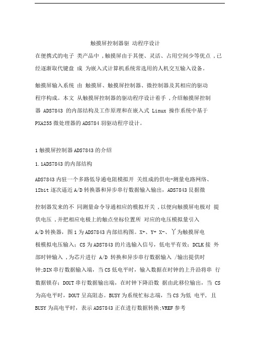
1触摸屏控制器ADS7843的介绍1.1ADS7843的内部结构ADS7843内驻一个多路低导通电阻模拟开关组成的供电-测量电路网络、12bit逐次逼近A/D转换器和异步串行数据输入输出,ADS7843艮据微控制器发来的不同测量命令导通相应的模拟开关 ,以便向触摸屏电极对提供电压 ,并把相应电极上的触点坐标位置所对应的电压模拟量引入A/D转换器,图1为ADS7843内部结构图。
X+、Y+ X-、丫为触摸屏电极模拟电压输入;CS为ADS7843的片选输入信号,低电平有效;DCLK接外部时钟输入 ,为芯片进行 A/D 转换和异步串行数据输入 /输出提供时钟;DIN串行数据输入端,当CS低电平时,输入数据在时钟的上升沿将串行数据锁存;DOUT串行数据输出端,在时钟下降沿数据由此移位输出,当 CS 为高电平时,DOUT呈高阻态。
BUSY为系统忙标志端,当CS为低电平, 且BUSY为高电平时,表示ADS7843正在进行数据转换;VREF参考电压输入端,电压值在+1V到+VCC之间变化;PENIRC为笔触中断,低电平有效;IN3、IN4为辅助ADC转换输入通道;+VCC为电源输入。
图1ADS7843内部结构1.2ADS7843的转换时序ADS7843完成一次数据转换需要与微控制器进行3次通信,第一次微处理器通过异步数据传送向 ADS843 发送控制字 ,其中包括起始位、通道选择、 8/12 位模式、差分 /单端选择和掉电模式选择 ,其后的两次数据传送则是微控制器从 ADS7843 取出 16bitA/D 转换结果数据(最后四位自动补零),每次通信需要 8 个时钟周期 ,完成一次数据转换共需 24 个时钟周期周2为ADS7843转换时序。
第十八节:ADS7843驱动的320240电阻型触摸屏:

资料范本本资料为word版本,可以直接编辑和打印,感谢您的下载第十八节:ADS7843驱动的320240电阻型触摸屏:地点:__________________时间:__________________说明:本资料适用于约定双方经过谈判,协商而共同承认,共同遵守的责任与义务,仅供参考,文档可直接下载或修改,不需要的部分可直接删除,使用时请详细阅读内容第十八节:ADS7843驱动的320240电阻型触摸屏(1)开场白:320240的触摸屏是由320240液晶显示屏和320240电阻触摸薄膜组成。
320240液晶显示屏披上一层触摸膜的皮就是触摸屏了。
显示和读取触摸信息是各自独立的,我们通过编写程序,两者有机结合起来,让客户产生错觉,以为触摸和显示是一体的。
320240液晶屏的程序在第十五节已经讲过。
现在重点介绍一下电阻触摸薄膜的原理。
它的本质是利用电阻分压的原理。
假如我在桌面上放了一条很长的裸露电阻,我们的手触摸到电阻的某点时,就相当于可调电阻的中间移动点,按到哪一点位置,我们只要通过AD把被分压后的电压读取出来,就知道你的手按到了哪个位置。
一张触摸膜相当于在X轴和Y轴都放了一个很宽很长的裸露电阻,手按到哪一点,只要把该点的X轴和Y轴的分压通过AD读取出来,就可以得到被触摸的X轴和Y轴坐标。
驱动电阻型触摸屏,就相当于单片机驱动一个外部AD转换芯片,这个AD芯片就是ADS7843。
编程技巧:我们要在显示屏上先做一个显示程序,专门用来显示按下去的X轴坐标和Y轴坐标,这样方便我们记录按键的位置信息。
有了具体某个按键的位置信息,我们才可以针对此按键进行后续的触发程序编写。
(2)功能需求:在触摸屏上按下一个矩形按键,此按键马上反显,表示被触发。
同时把相对应的X轴和Y轴坐标数据在液晶屏上显示出来。
(3)硬件原理:跟320240液晶显示屏的接线请参考第十五节。
然后用单片机的4个IO口分别跟ADS7843的DCLK, CS, DIN, DOUT连接。
51单片机程序触摸屏芯片ADS7843驱动

51单片机程序触摸屏芯片ADS7843驱动#include "reg51.h"#include "intrins.h"sbit DCLK=P1^6;sbit CS=P2^2;sbit DIN=P2^3;sbit DOUT=P2^4;sbit BUSY=P2^5;delay(unsigned char i--){while(i--);}void start() //SPI开始{DCLK=0;CS=1;DIN=1;DCLK=1;CS=0;}WriteCharTo7843(unsigned char num) //SPI写数据{unsigned char count=0;DCLK=0;for(count=0;count<8;count++){num<<=1;DIN=CY;DCLK=0; _nop_();_nop_();_nop_(); //上升沿有效DCLK=1; _nop_();_nop_();_nop_();}}ReadFromCharFrom7843() //SPI 读数据{unsigned char count=0;unsigned int Num=0;for(count=0;count<12;count++){Num<<=1;DCLK=1; _nop_();_nop_();_nop_(); //下降沿有效DCLK=0; _nop_();_nop_();_nop_();if(DOUT) Num++;}return(Num);}void ZhongDuan() interrupt 0 //外部中断0 用来接受键盘发来的数据{unsigned int X=0,Y=0;delay(10000); //中断后延时以消除抖动,使得采样数据更准确start(); //启动SPI// while(BUSY); //如果BUSY信号不好使可以删除不用delay(2);WriteCharTo7843(0x90); //送控制字 10010000 即用差分方式读X坐标详细请见有关资料// while(BUSY); //如果BUSY信号不好使可以删除不用delay(2);DCLK=1; _nop_();_nop_();_nop_();_nop_();DCLK=0; _nop_();_nop_();_nop_();_nop_();X=ReadFromCharFrom7843(); //读X轴坐标WriteCharTo7843(0xD0); //送控制字 11010000 即用差分方式读Y坐标详细请见有关资料DCLK=1; _nop_();_nop_();_nop_();_nop_();DCLK=0; _nop_();_nop_();_nop_();_nop_();Y=ReadFromCharFrom7843(); //读Y轴坐标CS=1;}main(){TMOD=0x11; // 记数器0 计数器1 都以 16 位记数TCON=0x00;IE=0x83; //1000 0001 EA=1中断允许,IP=0x01;while(1);//等待触摸中断}。
DEM-ADS7843E中文资料

SBAU0042®DEM-ADS7843E/45EINSTALLATIONThe DEM-ADS7843E/45E evaluation fixture is designed for stand-alone evaluation or evaluation using the clocking network on the board. Stand-alone evaluations imply that the A/D converter is powered by J4 (power supply connec-tor) and the user is put to the task to provide analog and digital input excitation. This is achieved by removing all five jumper tops of JP4 and using J1 and J2 for direct connec-tions to the device under test (DUT).In contrast, the DEM-ADS7843E/45E/45E board has the appropriate digital interface circuitry to drive the DUT data clock, chip select, and serial data in which is coordinated with the BUSY and PENIRQ to provide serial and parallel output data.This kit includes the following items:ADS7843E Evaluation Fixture—A2518DEM-ADS7843E/45E Documentation (LI-522)ADS7843E (5 samples)ADS7845E (5 samples)The DEM-ADS7843E evaluation fixture has two positions on the board for the A/D converter to be installed in. The first position is the socket, DUT1 on the board. This spring-loaded socket allows the user to quickly swap in or out the device that is being evaluated. The other option on the boardis the position X1, which is a solder location for the DUT. If this option is chosen, the user must solder the DUT directly to the board. This position is only useful for 2 or 3 solder cycles.CAUTION: DO NOT connect the a device into the DUT1 socket and have another device soldered to the board in position X1 at the same time.The additional equipment required to do a complete evalu-ation of the performance of the ADS7843E or ADS7845E comprises of:+5VDC power supplyV oltage or current signal source4-Wire (ADS7843E) or 5-Wire (ADS7845E) Resistive Touch ScreenTo install the DEM-ADS7843E/45E evaluation fixture, con-nect the appropriate power supply to J4. When power is applied to the DEM-ADS7843E/45E, the red LED on the board should light.USER CONFIGURATIONSThe DEM-ADS7843E/45E evaluation fixture provides the right combination of jumper options and support circuitry to allow for a variety of evaluation configurations. Throughout this data sheet, numerous references are made to the ADS7843and ADS7845 A/D converters. For more information con-cerning these devices, refer to the ADS7843 or ADS7845data sheet. The circuit is laid out with a four-layer board.The two outside layers are for circuit traces and the inner layers are the ground and power planes. The analog and digital planes of the circuit is separated through the middle of the board all the way to the power supply connector,where they are joined. The circuit diagram and layout diagrams for the DEM-ADS7843E/45E is shown in Figure 1 and Figures 4 through 7.J1Analog Input Interface. Each connector is labeled.J2Digital I/O Interface. Each connector is labeled.J3Parallel Output Port.J4Power Supply Connector. This connector powers the DUT and digital network. Refer to the ADS7843 or ADS7845product data sheet for power supply restrictions. All digital chips on the DEM-ADS7843E/45E board are capable of operating with supply voltage from 2.7V to 5.25V.P1External DCLK Connector.TABLE I. Connectors (Jx and P1) Assignments.JUMPER NUMBER FACTORY SETTINGDESCRIPTIONJP1BVoltage reference. This setting connects A/D converter reference to +V CC .JP2, JP11, JP10JP2 = Not Installed Inverted or non-inverted option for PENIRQ of the ADS7843 or ADS7845 when driving this pin through pin 2.JP11 = Not Installed This setting sets this pin HIGH and connects this pin to J2.JP10 = Not InstalledJP3D, F, G Hardwire digital jumpers for DIN serial code. This setting configures the A/D converter for S = HIGH, A2-A0 = 001, MODE = LOW, SGL/DIF = HIGH, PD1-PD0 = 11.JP4A, B, C, D, E This jumper connects the clocking network to the DUT.JP5, JP6JP5 = A Clock speed options. This configuration sets the board using Y1/10 as the DCLK frequency.JP6 = B JP7, JP8JP7 = B Optional 16- or 24-bit operation. This configuration sets the board for 16 DCLK per conversion cycle.JP8 = AJP9BUsed to personalize the board for the ADS7843 or ADS7845. Position B = ADS7843 or ADS7845.TABLE II. Jumper (JPx) Assignments.3®DEM-ADS7843E/45EDUT CONNECTIONSThe DEM-ADS7843E/45E DUT Board has a socket for the DUT which is positioned in the DUT1 position. Addition-ally, it has a solder footprint in the event that the user chooses to solder the DUT directly to the board. This footprint is poisitioned in X1, just below the DUT1 socket.If the solder footprint is used, care should be taken to preserve the solder pads for repeated soldering. Bad X1solder pads do not interfere with the operation or connec-tions of the DUT1 socket.The DEM-ADS7843E/45E evaluation fixture is designed to evaluate both the ADS7843 and ADS7845 A/D converters.JP9 must be in position B to evaluate either the ADS7843 or ADS7845.Space for an R/C input filter has been provided to allow user customization for the particular application. Shorting bars have been installed in R 3, R 5, R 7, R 9, R 10, and R 12 positions on the board. These are positioned betwen the input of the DUT and the pin connector, P1. Shorting bars were used to allow for immediate evaluation of a four-wire touch screen.In this situation, the touch screen would provide the source resistance. If resistors are desired in positions R 3, R 5, R 7, R 9,R 10, and R 12, the user can solder in the desired values.Additionally, positions for capacitors at the input of the DUT are provided with C 3, C 4, C 5, C 6, C 9 and C 10. Once again, the user must install appropriate values for the application under evaluation.The voltage reference to the DUT is programmed in the JP1.The JP1 options are given in Table III.The digital I/O pins of the DUT may be driven or monitored with the J2 connector. The assignment of these pins are summarized in Table V .POSITIONRESULTING CONFIGURATIONA 1.2V is configured to pin 9 (V REF ) of the DUT.B The power supply from J4 is configured to pin 9 (V REF )of the DUT.C2.5V is configured to pin 9 (V REF ) of the DUT.TABLE III. V REF is Programmed Using JP1 Position Options.The combination of JP2 allows jumper programmable set-tings of the PENIRQ of the ADS7843 or ADS7845 pin of the DUT. Additionally, this pin can be accessed through J2 and a combination of JP10 and JP11. Refer to Table IV for jumper position details. Refer to the ADS7845 data sheet for additional options.JP2 POSITION JP10 POSITION JP11 POSITION RESULTING CONFIGURATION Not Installed Not Installed Not Installed Pin 11 of the DUT is HIGH.Not Installed Installed Not Installed Pin 11 of the DUT is connected to position 5 of J2. If there is no connection to position 5 of J2, pin 11 of the DUT will default HIGH.Not InstalledNot InstalledInstalledPin 11 of the DUT is inverted and connected to position 5 of J2. If there is no connection to position 5 of J2, pin 11 of the DUT will default HIGH.Installed Not Installed Not Installed Pin 11 of the DUT is LOW.Installed Installed Not Installed Pin 11 of the DUT is connected to position 5 of J2. If there is no connection to position 5 of J2, pin 11 of the DUT will default LOW.InstalledNot InstalledInstalledPin 11 of the DUT is inverted and connected to position 5 of J2. If there is no connection to position 5 of J2, pin 11 of the DUT will default LOW.TABLE IV . PENIRQ (ADS7843 or ADS7845) Jumper Settings.J2 PIN NUMBER (From Left to Right)ADS7843 PIN DESCRIPTION1CS 2DCLK 3BUSY 4DIN 5PENIRQ 6DOUTTABLE V .J2 Connector Contacts versus DUT Pins.(NOTE: If you have a DEM-ADS7843E/45E,Revision A, the silkscreen is in error. The above description is correct.)STAND-ALONE OPERATIONThe DUT can be evaluated in a stand-alone configuration by removing all of the jumper tops of JP4. JP4 connects pins 12,13, 14, 15, and 16 of the DUT to the digital interface circuitry of the board. If the array of jumper tops are not removed, the user may find significant conflicts on the digital I/O lines of the DUT. The details of this interface circuitry is discussed in detail in the “Digital Interface”section of this data sheet.DIGITAL INTERFACE CIRCUITRYThe DUT can be evaluated using the digital clocking cir-cuitry on the board by installing all of the jumper tops of JP4and removing any signal present on the J2 connector. This digital circuit uses the clock signal from P1 (External Clock)or Y1 to create the DUT clock (DCLK), CS, and the DIN code to the device while providing a serial or parallel output signal from the DOUT pin of the DUT.Clock ControlThe master clock to the board is set with the JP6 jumper.Position A of the JP6 jumper configures the External Clock (P1) coax connector into the circuit. It is recommended that this signal be a logic square wave. The signal from this connector will be used directly for the DCLK signal to the4®DEM-ADS7843E/45EDUT. Refer to the ADS7843 or ADS7845 data sheet for the proper restrictions on this clock. Alternatively, a clock oscil-lator that is installed in Y1 can be used as the master clock.The signal from this device is either divided by 10 or divided by 20 per JP5. The settings from JP5 are listed in Table VI.JUMPER SETTINGRESULTING CONFIGURATIONAY1 Frequency divided by 10. In conjunction with JP6 = B, this frequency becomes DCLK for the DUT.BY1 frequency divided by 20. In conjunction with JP6 = B, this frequency becomes DCLK for the DUT.TABLE VI. Jumper Settings for Using Y1 as Master Clock.Clocks per Conversion ControlOnce DCLK is set (per clock control instructions) the conversion cycle of the DUT can be configured to either take 16 or 24 clock cycles. The jumper configuration for these two modes of operation are shown in Table VII. Addition-ally, the timing diagram of these two modes of operation are shown in Figures 2 and 3.JP7JP8RESULTING CONFIGURATION A B 24 DCLK cycles per conversion BA16 DCLK cycles per conversionTABLE VII. The Digital Support Circuitry Can be Operatedin a 16 Clocks per Conversion or a 24 Clocks per Conversion with the Jumper Settings De-scribed in the Table. Refer to Figures 2 and 3for specific timing.DIN ProgrammingThe DIN input (DUT, pin 14) receives an 8-bit serial input data stream which programs the ADS7843 or ADS7845 X or Y input channel, mode and power-down options. This serial stream can be programmed with JP3. JP3 is essentailly an 8-bit parallel configuration which is processed by a parallel-to-serial converter (U8) and then transmitted to the DUT at the appropriate time. Even when a position on JP3 is jumper top configured, digital gates can over drive their settings. Con-sequently, these lines are also connected to the digital breadboard area, which gives the user more flexibility in terms of programming this serial command byte.Parallel OutputThe combination of U13 and U14 converts the digital output of the DUT into a parallel word. This parallel word appears on the connector J3. A DV ALID trigger is also provided on J3. Refer to Table VIII for the J3 connector configuration.J3 PIN DESCRIPTION1DVALID 11LSB 13LSB + 115LSB + 217LSB + 319LSB + 421LSB + 523LSB + 625LSB + 727LSB + 829LSB + 931LSB + 1033MSB 3, 5, 7, 9Digital LOW 35 through 50Open All Even PinsGNDTABLE VIII. J3 Configuration.5®DEM-ADS7843E/45EPARTNUMBER PART LOCATIONPER KITNUMBER VENDORDESCRIPTION 1A-2518 Rev B ADS7843E Bare BoardX1 (not installed)1Accepts ADS7843E Burr-Brown 12-bit A/D converter solder land area, parts not installed and ADS7845E U11REF1004C-1.2Burr-Brown 1.235V Reference, SOIC U21REF1004C-2.5Burr-Brown 2.5V Reference, SOICDUT 5ADS7843E Burr-Brown 12-bit Touch Screen A/D Converter (4-wire panel)DUT 5ADS7845E Burr-Brown 12-bit Touch Screen A/D Converter (5-wire panel)DUT (socket)1OTS-16(24)-0.635-01Enplas (TESCO)16-lead SSOP socket U3, U5, U7374HC393D TI (1)Dual, 4-bit, binary counterU4174HC08D TI (1)Quadruple two-input positive AND gates U6174HC04D TI (1)Hex InvertersU8174HC166D TI (1)8-bit parallel-load shift registerU13, U142SN74HC594D TI (1)8-bit shift registers with output registers U151MC74HC390D TI (1)Decade counter, dual 4-bit Y11CTX129-ND DigiKey 32MHz clock oscillator, (CTS)Y1 (socket)11107741Aries 14-pin oscillator socket, DIP D11HLMP-3201Hewlett Packard (1)Red LEDR 3, R 5, R 7, R 9, R 10, R 12Optional. Provided with shorts. Resistors not included.R 131CRCW12062001F Dale 2k Ω, 1%, 0.125W, metal-film resistor R 141CRCW12061001F Dale 1k Ω, 1%, 0.125W, metal-film resistor R 15, R 162CRCW120622R1F Dale 22.1k Ω, 1%, 0.125W, metal-film resistor R 1, R 112CRCW12061002F Dale 10k Ω, 1%, 0.125W, metal-film resistor R 8, R 182CECW12061003F Dale 100k Ω, 1%, 0.125W, metal-film resistor R 2, R 4, R 63CRCW12061000F Dale 100Ω, 1%, 0.125W, metal-film resistor R 171CRCW12066810F Dale 681Ω, 1%, 0.125W, metal-film resistor C 11T491B225K016ASKemet2.2µF capacitor, 16VC 3 through C 6, C 9, C 10Optional. Capacitor not included.C 12, C 14 through C 2513C1206C104K5RAC Kemet 0.1µF surface-mount capacitor, X7R C 11, C 132T491C106K016AS Kemet 10µF polarized capacitors, 16V, 10%C 21C1206C103K5RAC Kemet 0.01µF, 50V, 10%, chip-ceramic, X7R C 81C320C104K5R5CA Kemet 0.1µF, 50V, 10%, ceramic JP11TSW-103-07-T-D Samtec 2 x 3JP21TSW-101-07-T-D Samtec 2 x 1JP31TSW-108-07-T-D Samtec 2 x 8JP41TSW-105-07-T-D Samtec 2 x 5JP5 through JP95TSW-103-07-T-S Samtec 1 x 3JP1, JP2, JP3 tops 3SNT-100-BK-T Samtec Jumper TopsJ1, J2, J4 pins 731024102RIACON 2-pin terminal block pins, 3.5mm centers J1, J2, J4 tops 731165102RIACON 2-pin terminal block tops, 3.5mm centersJ31IDH-50LP-S3-TGRobinson Nugent2 x 25, straight-through header w/shroud, 0.1" center spacing P1147788Pamona BNC right-angle, PC mount connector RN21CSC10A-01-104F Dale 10-pin SIP resistor network (100k Ω, 9R, 1C)RN11CSC10A-01-103F Dale 10-pin SIP resistor network (10k Ω, 9R, 1C)Rubber Feet6SJ5523-O-ND3MBumponsNOTE: (1) Or equivalent.TABLE IX. Parts List for the DEM-ADS7843E/45E.6®DEM-ADS7843E/45EFIGURE 1a. ADS7843E and ADS7845E Evaluation Demo Board Analog Circuit Diagram.7®DEM-ADS7843E/45EFIGURE 1b. ADS7843E and ADS7845E Evaluation Demo Board Digital Circuit Diagram.8®DEM-ADS7843E/45EFIGURE 2. ADS7843E and ADS7845E Conversion Timing Diagram, 16 Clocks per Conversion.FIGURE 3. ADS7843E and ADS7845E Conversion Timing Diagram, 24 Clocks per Conversion.9®DEM-ADS7843E/45EFIGURE 4. Component Side of the DEM-ADS7843E/45E Demonstration Board.FIGURE 5. Ground Plane of the DEM-ADS7843E/45E Demonstration Board.10®DEM-ADS7843E/45EFIGURE 6. Power Plane of the DEM-ADS7843E/45E Demonstration Board.FIGURE 7. Solder Side of the DEM-ADS7843E/45E Demonstration Board.11®DEM-ADS7843E/45EFIGURE 8. Component Side Silkscreen of the DEM-ADS7843E/45E Demonstration Board.FIGURE 9. Component Side Soldermask of the DEM-ADS7843E/45E Demonstration Board.12®DEM-ADS7843E/45E FIGURE 10. Bottom Side Soldermask of the DEM-ADS7843E/45E Demonstration Board.IMPORTANT NOTICETexas Instruments and its subsidiaries (TI) reserve the right to make changes to their products or to discontinue any product or service without notice, and advise customers to obtain the latest version of relevant information to verify, before placing orders, that information being relied on is current and complete. All products are sold subject to the terms and conditions of sale supplied at the time of order acknowledgment, including those pertaining to warranty, patent infringement, and limitation of liability.TI warrants performance of its semiconductor products to the specifications applicable at the time of sale in accordance with TI’s standard warranty. Testing and other quality control techniques are utilized to the extent TI deems necessary to support this warranty. Specific testing of all parameters of each device is not necessarily performed, except those mandated by government requirements.Customers are responsible for their applications using TI components.In order to minimize risks associated with the customer’s applications, adequate design and operating safeguards must be provided by the customer to minimize inherent or procedural hazards.TI assumes no liability for applications assistance or customer product design. TI does not warrant or represent that any license, either express or implied, is granted under any patent right, copyright, mask work right, or other intellectual property right of TI covering or relating to any combination, machine, or process in which such semiconductor products or services might be or are used. TI’s publication of information regarding any third party’s products or services does not constitute TI’s approval, warranty or endorsement thereof.Copyright © 2000, Texas Instruments Incorporated。
基于ADS7843的触摸屏控制系统设计

Science &Technology Vision科技视界0引言在电子产品及工业产品的设计中,触摸屏由于其轻便、占用空间少、方便灵活等优点越来越受到设计师及用户的青睐。
触摸屏可作为模拟键盘,使用起来比普通键盘灵活,因为键的位置可根据需要进行改变,并且省去了按键所占用的空间。
触摸屏分为电阻、电容、表面声波、红外线扫描和矢量压力传感等,其中四线电阻触摸屏应用广泛。
1ADS7843简介ADS7843是一款专为四线电阻触摸屏设计的带SPI 接口的12位AD 转换器,内部含模拟电子开关和逐次比较型AD 转换器。
当要采样Y 方向的AD 值时,通过将Y+、Y 一端施加电压,将X+送入AD 转换器得到Y 方向的AD 值;同理可得X 方向的AD 值。
而这些转换均由MCU 通过SPI 方式向ADS7843发送命令来完成。
ADS7843的引脚功能如表1所示。
表1ADS7843的引脚功能ADS7843之所以能实现对触摸屏的控制,是因为其内部结构很容易实现电极电压的切换,并能进行快速A/D 转换。
内部结构如图1所示,A2~A0和SER 为控制寄存器中的控制位,用来进行开关切换和参考电压的选择。
图1ADS7843内部结构2触摸屏控制系统设计以应用广泛的STC89C52作为主控制器,进行触摸控制系统设计。
2.1硬件接口电路设计ADS7843串行接口的一次完整操作需要3×8=24个DCLK 时钟周期,前8个脉冲接收8位的命令,并在第6个脉冲的上升沿开始A/D 转换器进入采样阶段,从第9个脉冲开始进入转换阶段,输出,输出12位采样值,转换结束进入空闲阶段。
直到24个DCLK 结束,CS 置高电平,一次测量结束。
ADS7843采用、转换时序如图2所示。
图2ADS7843采用、转换时序ADS7843与STC89C52的连接图如图3所示。
图3ADS7843与STC89C52的连接图2.2软件设计当用户在触摸屏上的有效区域内点击时,触摸屏的X 方向、Y 方向输出电阻分别随X 和Y 呈线性变化,ADS7843控制器将其分别转换为12位数据,通过中断告知STC89C52需要接收数据,STC89C52接收到数据后进行处理;首先进行触点数据是否有效判断,包括两方面:一是判断是否误操作,即是否是由于人的抖动产生的错误数据;二是ADS7843传过来得数据是否有效,由于刚开始的传过来的第一个基于ADS7843的触摸屏控制系统设计薛大为杨春兰(蚌埠学院机械与电子工程系,安徽蚌埠233030)【摘要】触摸屏在现代电子设备中广泛使用。
- 1、下载文档前请自行甄别文档内容的完整性,平台不提供额外的编辑、内容补充、找答案等附加服务。
- 2、"仅部分预览"的文档,不可在线预览部分如存在完整性等问题,可反馈申请退款(可完整预览的文档不适用该条件!)。
- 3、如文档侵犯您的权益,请联系客服反馈,我们会尽快为您处理(人工客服工作时间:9:00-18:30)。
触摸屏控制芯片ADS7843中文资料
ADS7843是一个内置12位模数转换、低导通电阻模拟开关的串行接口芯片。
供电电压2.7~5 V,参考电压VREF为1 V~+VCC,转换电压的输入范围为0~ VREF,最高转换速率为125 kHz。
ADS7843引脚图及引脚功能说明了:
ADS7843的引脚配置如图3所示。
表1为引脚功能说明,图4为典型应用。
aDS7843引脚说明
ADS7843典型应用电路
2.2 ADS7843的内部结构及参考电压模式选择
ADS7843之所以能实现对触摸屏的控制,是因为其内部结构很容易实现电极电压的切换,并能进行快速A/D转换。
图5所示为其内部结构,A2~A0和SER/为控制寄存器中的控制位,用来进行开关切换和参考电压的选择。
ADS7843支持两种参考电压输入模式:一种是参考电压固定为VREF,另一种采取差动模式,参考电压来自驱动电极。
这两种模式分别如图6(a)、(b)所示。
采用图6(b)的差动模式可以消除开关导通压降带来的影响。
表2和表3为两种参考电压输入模式所对应的内部开关状况。
2.3 ADS7843的控制字及数据传输格式
ADS7843的控制字如表4所列,其中S为数据传输起始标志位,该位必为"1"。
A2~A0进行通道选择(见表2和3)。
MODE用来选择A/D转换的精度,"1"选择8位,"0"选择12位。
SER/选择参考电压的输入模式(见表2和3)。
PD1、PD0选择省电模式:
"00"省电模式允许,在两次A/D转换之间掉电,且中断允许;
"01"同"00",只是不允许中断;
"10"保留;
"11"禁止省电模式。
为了完成一次电极电压切换和A/D转换,需要先通过串口往ADS7843发送控制字,转换完成后再通过串口读出电压转换值。
标准的一次转换需要24个时钟周期,如图7所示。
由
于串口支持双向同时进行传送,并且在一次读数与下一次发控制字之间可以重叠,所以转换速率可以提高到每次16个时钟周期,如图8所示。
如果条件允许,CPU可以产生15个CLK 的话(比如FPGAs和ASICs),转换速率还可以提高到每次15个时钟周期,如图9所示。
2.4 A/D转换时序的程序设计
ADS7843的典型应用如图4所示。
假设μP接口与51单片机的P1.3~P1.7相连,现以一次转换需24个时钟周期为例,介绍A/D转换时序的程序设计。
; A/D 接口控制线
DCLK BIT P1.3
CS BIT P1.4
DIN BIT P1.5
BUSY BIT P1.6
DOUT BIT P1.7
; A/D 通道选择命令字和工作寄存器
CHX EQU 094H ;通道X+的选择控制字CHY EQU 0D4H;通道Y+的选择控制字
CH3 EQU 0A4H
CH4 EQU 0E4H
AD_CH EQU 35H ;通道选择寄存器
AD_RESULTH EQU 36H ;存放12 bit A/D值AD_RESULTL EQU 37H
; 存放通道CHX+的A/D值CHXAdResultH EQU 38H
CHXAdResultL EQU 39H
; 存放通道CHY+的A/D值CHYAdResultH EQU 3AH
CHYAdResultL EQU 3BH
; 采集通道CHX+的程序段(CHXAD) CHXAD: MOV AD_CH,#CHX
LCALL AD_RUN
MOV CHXAdResultH,AD_RESULTH
MOV CHXAdResultL,AD_RESULTL
RET
; 采集通道CHY+的程序段(CHYAD)
CHYAD: MOV AD_CH,#CHY
LCALL AD_RUN
MOV CHYAdResultH,AD_RESULTH
MOV CHYAdResultL,AD_RESULTL
RET
; A/D转换子程序(AD_RUN)
; 输入: AD_CH-模式和通道选择命令字
; 输出: AD_RESULTH,L ;12 bit的A/D转换值; 使用: R2 ;辅助工作寄存器
AD_RUN:
CLR CS ; 芯片允许
CLR DCLK
MOV R2,#8 ;先写8 bit命令字
MOV A,AD_CH
AD_LOOP:
MOV C, ACC.7
MOV DIN,C ;时钟上升沿锁存DIN
SETB DCLK ;开始发送命令字
CLR DCLK ;时钟脉冲,一共24个
RL A
DJNZ R2,AD_LOOP
NOP
NOP
NOP
NOP
ADW0: JNB BUSY,AD_WAIT ;等待转换完成SJMP ADW1
AD_WAIT:
LCALL WATCHDOG
NOP
SJMP ADW0
CLR DIN
ADW1: MOV R2,#12 ;开始读取12bit结果SETB DCLK
CLR DCLK
AD_READ:
SETB DCLK
CLR DCLK ;用时钟的下降沿读取
MOV A,AD_RESULTL
MOV C,DOUT
RLC A
MOV AD_RESULTL,A
MOV A,AD_RESULTH
RLC A
MOV AD_RESULTH,A
DJNZ R2,AD_READ
MOV R2,#4 ;最后是没用的4个时钟
IGNORE:
SETB DCLK
CLR DCLK
DJNZ R2,IGNORE
SETB CS ;禁止芯片
ANL AD_RESULTH,#0FH ;屏蔽高4 bit
RET
2.5 A/D转换结果的数据格式
ADS7843转换结果为二进制格式。
需要说明的是,在进行公式计算时,参考电压在两种输入模式中是不一样的。
而且,如果选取8位的转换精度,1LSB=VREF/256,一次转换完成时间可以提前4个时钟周期,此时串口时钟速率也可以提高一倍。
点击查看:ads7843 datasheet
点击查看:ADS7843驱动程序
--------------------------------------------------------------------------------
相关文章
MTK各芯片功能及平台介绍
展讯3G手机芯片:SC8800系列TD-
展讯(MTK)手机芯片:SC6800系列
展讯(MTK)手机芯片:SC6600系列
触摸屏控制芯片ADS7843中文资料
锂电池充电器芯片MAX1811中文资料
CN3059的原理及应用介绍
ML2035中资料(单片正弦波发生器芯片
MAX705,MAX831L,MAX70
MAX813L/MAX705中文资料
(注:素材和资料部分来自网络,供参考。
请预览后才下载,期待你的好评与关注!)。