K60(Rev6-Ch14-Power Management Controller)(中文)
K60(Rev6-Ch55-TSI)(中文)
第55 章触屏输入(Touch senseinput ,TSI)55.1 引言触摸感应输入(TSI)模块具有高灵敏和强鲁棒性的电容触摸感应检测能力。
通过独立的可编程的检测阈值和结果寄存器,TSI模块可以完成电容的测量。
TSI 模块在带有超低电流加法的低功耗模式下运行,能以一个触摸事件唤醒CPU。
它是一种稳定的电容测量模块,能够实现键盘触摸,旋转和滑动。
55.2 特点(1)具有多达16个输入的电容触摸感应式引脚和独立结果寄存器(2)具有可编程的阈值上下限,自动检测电极电容量的改变(3)在运行模式和低功耗模式下,自动周期扫描单元会有不同的占空比(4)为了实现键盘触摸,旋转,滑动,完全支持FSL触摸感应SW库(TTS)。
(5)运行在所有低功耗模式下:Wait, Stop, VLPR, VLPW, VLPS,LLS,VLLS{3,2,1}(6)能够从低功耗模式中唤醒MCU(7)配置中断:a.扫描结束中断或者超出范围中断b.TSI错误中断:电极板和VDD/VSS短路或者转换运行超时(8)补充温度和提供电压变化(9)在低功耗模式下,支持不需要外部晶体的操作,(10)每个电极电容量测量可以整合从1到4096次(11)可编程的电极振荡器和TSI参考振荡器可以实现模块灵敏度高,扫描时间短和功耗低的功能(12)在不需要外部硬件时,实现每个电极电容测量只需要使用一个引脚55.3 总述这部分是对TSI模块的总述。
下图给出了简化了的TSI模块结构图。
图55-1 触摸感觉输入结构图55.3.1 电极电容测量单元电极电容测量单元能感应一个TSI引脚的电容量变化和输出一个16位结果。
这个模块基于双振荡器架构。
其中一个振荡器和外部电极阵列连接,根据电极电容器震荡;而其他振荡器则根据内部参考电容器进行振荡。
在可配置的外部电极振荡器振荡期间,参考振荡器的周期计数值可以衡量引脚的电容量。
图55-2 TSI电容衡量单元结构图为了适应电极电容量的不同大小,电极振荡器使用一个可编程的电流源对引脚电容进行充电和放电,该电流源由SCANC[EXTCHRG]位进行选择。
K60A电压用户指南说明书

K60A Voltage User GuideAugust 5 2010, Second EditionWARNING: SAFETY FIRSTFor safety reasons and to avoid personal injury, read all operating guides and information in the product guide. DO NOT attempt to modify Mentor device and sensors in any way. This may result in fire, injury, electric shock or severe damage to you or them.1.DO NOT operate Mentor device and sensors with wet hand, this may cause anelectric shock.2.DO NOT use Mentor device and sensors in close proximity to flammable or explosivegases, or chemical vapors. Use this product in a well ventilated area.3.For safety reasons keep this sensor out of reach of children or animals to preventaccidents, for example swallowing small size of the sensor. DO NOT allow children to play on or around the sensor.4.DO NOT use the sensor to check AC power circuits. DO NOT use the sensor in ACpower outlet or sockets, this may cause a hazardous injury to you.CAUTION:1.DO NOT use Mentor device and sensors in extreme conditions which are over theoperating range and short-term exposure limit conditions. Stresses above input range may cause permanent damage.2.Exposure to absolute maximum conditions for extended periods may degrade sensorreliability.3.The sensors are permanently sealed during construction and cannot be opened toany purpose. DO NOT attempt to decompose, modify or repair the sensor in any other ways. This may cause permanent damage to the sensor.4.Liquids shall not come into direct contact with the sensor. DO NOT place sensor orcable in water, liquids, flame or on a hot plate.5.DO NOT use this sensor in close proximity to flammable or explosive gases. Chemicalvapors may interfere with the polymer layers used for capacitive this sensor and high levels of pollutants may cause permanent damage to this sensor.Features and Specifications FeaturesItem DescriptionFeature Two voltage clips with electric patch cords: red testclip(+), black test clip(-)Non volatile memory supported for user calibration. Dimension Sensor base housing: 42x18x16 (WxDxH) in mmAlligator clip: 6cm(L),Electric patch cords l : 35cm(L), 3mm(φ)Usage Use only in a dry place at room temperature below+40°C.SpecificationsItem DescriptionInput range Differential: - 15V to +15VResolution 14bit spacing amplitude, Typ. ±2mV, Max. ±3mVAccuracy Typ. ±10mV, Min.±5mV @<±1.0V, Max. ±30mV Measurement deviation from linear correlation: -In full scale range: Typ.±0.2%-In lower range: Typ. ±0.05% @<±1.0VSampling rate1Default sampling periods: 0.2s (5samples/sec) Max.20samples/sMax. over voltage2±30VInput impedance 5.3±1.5% MΩ @25°CCalibration Factory calibration stored and FC values recovery supported to restore factory calibration.Optional user calibration data can be wrote to non-1If you need the sampling rate up to 1000samples/s, use the voltage sensor K60B. Or if you use the oscilloscope probe, you can view the waveform graph for voltage with max. 200kHz sampling rate in ±10V range.2Maximum overload voltage without damage, stress above this range may cause permanent damage.Item Descriptionvolatile user memory.User calibration methods: 1 or 2 points linearcalibrationZero offset Zero-voltage offset drift: Typ. ±1mV@25°CZero setting with non-volatile memory supported.NOTE:You do not need the calibration when using the voltage sensor. But if you calibrate the sensor for your any purpose, the calibration data created by user does not erased after disconnecting the sensor or power off Mentor. The data for calibration or zero setting with MentorStart is wrote to non-volatile memory in the sensor.Additional equipment or applicationMentor device and MentorStart application software needed. If you are using Mentor application, consult your instructor for more information. CAUTION:1.DO NOT connect this sensor to over voltage anywhere in the circuit orpower source. The voltage should NOT exceed +15V above or below earth ground.2.Always use the sensor on a known live voltage under the maximum inputrange before proceeding with your test and measurements.3.Make sure you are reasonably well grounded and isolated from the cableor any piece of equipment you are measuring.4.In some cases, the sensor may falsely indicate the voltage value due to anincorrect circuit you use.Setup and Usageunch the MentorStart software and connect the sensor to the sensorport in your Mentor device. MentorStart will automatically detect the sensor.2.To measure the voltage between the V+(red) clip and the V-(black) clip,connect the voltage clips across a battery, DC power source, or circuit elements.To measure the voltage with a voltmeter-like readingWhen you are reading one-shot data with Snapshot mode, you can use the sensor as a voltmeter which can be used to measure negative or positive potential difference.Fig.1 Testing a battery voltage with the Voltage sensor. You can check and test the most common type of household battery. For example, an AA battery is commonly used in electronic devices. When you replace the battery with an equal replacement battery to assure proper operation of your electronic device, you can check the battery which has enough voltage to power the device or not. In this activity, the voltage between the plus and minus on the battery have been referred to as EMF voltage generated by the battery.NOTE: The Voltage sensor is always connected in parallel with the part of the circuit to measure the potential difference across a circuit element.Fig.2 Testing the voltage with a voltmeter-like one shot reading after settingZero to the voltage sensor.Voltage and current measurementIn an application of Ohm’s law, you can measure the voltage across anelectrical resistance or Ohmic materials with the Voltage sensor and thecurrent through it with the Current sensor. When you measure the current,the Current sensor is placed always in series and the Voltage sensor isconnected in parallel. For an example of measuring the voltage and current,you use two 1.5volts batteries and the red LED3 (See Fig.3 and Fig.4).3 You can choose a LED referred to the supplier’s catalogues. You might check the parameters such as the forward voltage and current, and then you use a proper resistor for LED.Fig.3 Measure the voltage and the current through LED. Using Ohm’s law which works even for non-Ohmic materials where the resistance depends upon the current, you can calculate the resistance for LED.Fig.4 Voltage and Current measurement with the Voltmeter/Ammeter-like one-shot reading.Guide to Physics ExperimentsTable.1 Science experiments using the Voltage sensor.Students’ activity with practical physics experiments1 Measure the voltages across electrical elements in parallel2 Test the Voltage law4 and explore the Current law3 Test the Ohm’s law and explore the relationship5 between the voltageand the current4 Measure the power dissipated in a resistor5 Measure the DC power voltage in series or parallel circuits6 Test the combination rules for any number of resistors in series orparallel circuits7 Measure the charging or discharging voltage on a capacitor8 Investigate the behavior of LED or electrolytes with everydayhousehold materialsMeasure the voltage across a resistor in seriesIn this activity, students can easily demonstrate the voltage law with therelationship between the voltage and the electrical resistance which isdefined as the ratio of the voltage applied to the electric current while thecurrent flows through the resistance and the value of the current is the samein each resistor by the current law. Whether or not your material obeysOhm’s law, you can measure the potential difference with the resistors. Asyou can see Fig.1 shown below, you can make the combination for a numberof the resistors in series and you can measure the voltage across each or anynumber of resistors by the voltage law as the following calculation:V=V1 + V2 + V3 + … Vn4The voltage law is expressed as the net voltage drop around any closed loop path must be zero. See the reference from: /hbase/hframe.html5 A correlation between voltage and current is an important problem that students critically face during a physics concept developing by inquiry. For example, a student correlates the direct relationship that voltage is the required energy that drives the flow of current which will flow through conductorsWhere V is the sum of the voltages around any closed loop, V1, V2, … Vn are the voltage drops across the resistors r1, r2,…rn.Fig.1 Testing the voltage law with the combination rules for a number of the resistors in series. Each resistor has 1kΩ and the voltage of a battery is 1.5V. Exploring the transient behavior of a capacitorIn this experiment, if you connect the battery using the clip B+ and B- to the circuit as Fig.2 shown, the capacitor will be fully charged up to the battery voltage and the voltage reading will has a constant value of the maximum voltage. Just after then, if you disconnect the battery and join two clips of (B+)and (B-) together, the voltage reading will follow a type of an exponential decay curve. The mathematical model of a charging or discharging capacitor can be formed as the followings:V=Vb[1-exp(-t/RC)]… Charging capacitorV=Vc*exp(-t/RC)… Discharging capacitorwhere V is the changing voltage, R is the resistance and C is the capacitor. The voltage rate of charging or discharging can be described in terms of a time constant RC.Fig.2Testing the voltage rate for charging or discharging a capacitor. The resistor has 3000Ω and the capacitor is 1000μF.Table.1 Analysis results of decaying curve fit for discharging a capacitor. The mathematical formula of this decaying model is V=Vc*exp(-(t’+t0)/RC))+V0. For circuit parameters in this experiment, the theoretical value of RC is 0.333 where R=3000Ω and C=0.001F, and the calculated value with the decaying model is 0.327.Parameters Analysis resultst0 30.2t1 38.4dt (Sampling periods in seconds) 0.2Vc (Coefficient of best fit) 0.796Parameters Analysis results Theoritical value of (1/RC) 0.333 Calculated value of (1/RC) with0.327 exponential decaying modelV0 (Intercept of best fit) 0.018R-squared 0.999RMSE(Fit standard error) 0.015Fig.3 Voltage measurement graph of charging and discharging capacitor. You connect two voltage clips to the battery, and after reading the maximum voltage continuously, join two clips together to discharge the capacitor.You can fit the exponential curve with MentorStar t program as Fig.4 shown below and report the results if the curve fit, for example as you see Table.1.Fig.4 Exponential fit of decaying curve with MentorStart. When you press the curve fit icon on the screen of MentorStart, you can choose the equation of your model, y=A*exp(B*x)+C and calculated the parameters in the Table.1 above. To view the results of analysis, press the viewing results icon on the screen of MentorStart, not only you can get the results of the parameters such as the coefficients A, B and C with the fitting model, y=A*exp(B*x)+C, but also when you are trying to analyze the charging curve of a capacitor, you can choose the exponential model: y=A*(1-exp(B*x))+C.NOTE: To get the best fit of the measurement data, you predict the equation and choose the proper curve fitting model on the screen of MentorStart. Testing Ohm’s law with ohmic or non-ohmic materialsIn this activity, you measure the voltage and the current through the resistor, test and describe the relationship of Ohm’s law. The slopes in Fig.5 shown below tell us how an unknown resistance can be measured with a closed circuit and this makes it very easy to represent and apply Ohm’s law.Fig.5 Measurement chart of voltage versus current. To test Ohm’s law, youuse the Voltage senor and the Current6 or Galvanometer sensor. As the DCpower source, you use the battery or power supply. Each slope of the linearfit equation on voltage versus current chart shows the resistance of 56Ω,152Ω and 498Ω.In this activity, it is helpful to discuss the properties of the ohmic or non-ohmic materials7 in terms of the relationship between the resistance and thevoltage across it. Students inquire the relationship between the voltage andthe current depends on the source of electricity and materials being used inthe circuit.6In according to the results of the testing Ohm’s law, you can describe a logistic equation as the following: i=(E-V)/r, where E is the EMF voltage of power source, V is the voltage drop through the test resistor and r is a very small equivalent resistance due to dissipation of the Current sensor.7Although you use non-ohmic materials, you can use Ohm’s law to calculate the resistance across the non-ohmic materials. For example, you use LED and you can measure the voltage drop through LED.LIMITED WARRANTYPlease check that this product is operating properly prior to when you intend to use it for educational purposes only. Use this device and sensors for teaching and learning. The information given in this electronic document shall not be regarded as a guarantee or warranty of physical characteristics and any conditions. We will not replace or cover the costs of a damaged sensor or probe due to negligent or destructive, improper use.Korea Digital Co., Ltd.©2009 Korea Digital, All rights reserved.707, Ace Twin Tower1804, Ace Twin Tower2Guro Digital Complex, Seoul, Korea+82-2-2109-8877 (Tel)+82-2-2109-8878 (Fax)ScienceCube Mentor is a trademark ofKorea Digital, Co., Ltd.Designed by Korea Digital in KoreaFor more information about installingMentor, using other applications andgetting the feedbacks, contact:ScienceCube international distributor.If you have any questions about a guideto physics experiment using the sensor,please contact author at *************。
K60 介绍 (中文)
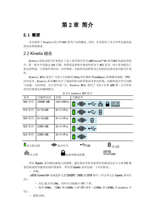
第2章简介2.1 概要本章提供了Kinetis组合和K60系列产品的概述。
同时,本章提供了本文件所包涵设备的高水准的描述。
2.2 Kinetis组合Kinetis是低功耗可扩展和在工业上使用混合信号ARM®Cortex™-M4系列MCU的最好的组合。
第一部分介绍超过200引脚、外围设备和软件兼容性的5个MCU系列。
每个系列提供了优良的性能,与普通外设内存,内存映射,并提供内部和系列之间轻松迁移包和功能可扩展性。
Kinetis MCUs使用了飞思卡尔的新的90nm带有独特FlexMemory的薄膜存储器(TFS)闪存技术。
Kinetis系列MCU结合了最新的低功耗革新技术和高性能,高精密混合信号功能与连通,人机界面,安全及外设广泛。
Kinetis MCUs使用了飞思卡尔和ARM第三方合作伙伴的市场领先的捆绑模式。
表示低功耗混合信号USB 段LCD以太网加密和篡改检测DDR所有Kinetis系列都包涵强大的逻辑、通信和时序阵列和带有伴随着闪存大小和I/O数量的集成度等级的控制外围部件。
所有的kinetis系列包涵一下共同特征:· 内核:· ARM Cortex-M4内核提供1.25 DMIPS / MHz的DSP指令(浮点单元在kinetis系列可用)。
· 高达32位的DMA,同时尽可能减小CPU干预。
· 提供50MHz、72MHz和100MHz几种CPU频率(120MHz和150MHz在kinetis可用)。
· 超低功耗:· 10种低功耗操作模式通过优化外设执行和唤醒时间来延长电池寿命。
· 为了增加低功耗的灵活性,增加了低漏唤醒单元、低功耗定时器和低功耗RTC。
· 业界领先的快速换醒时间。
· 内存:· 从32 KB闪存/ 8 KB的RAM可扩展为1 MB闪存/128 KB的RAM。
同时使空白的独立闪存执行代码和固件更新。
关于60KW控制器的相关研究和实验结果剖析

用户反映故障状态数据采集如下:
一、控制器在安装使用中常常遇到,客户在安装加热线圈时出现安装规
范不标准,线圈没有按说明书提示绕制,造成电感量太小或者保温棉 太薄,等因素,造成控制器上电工作几分钟出现E02故障代码。
二、
控制器在使用一段时间后,会发生E04的报警,或者E05的故障代码。 经与客户沟通了解到出故障时无规律无异常。实际电压测量低于报警电压值或高 于报警电压,都在报警电压范围内。从而使客户工作效率大大下降,和经济利益 受到损失。
实验结束
•
注 本论文最终解释权归上海汇信有限公司所有 : 2015年09月14日 由于编写者水平有限,请提宝贵意见
三、在使用部分客户反映控制器使用一段时间会出现功率下降,效率低下,加热
时间长,温度提升慢。据实际测量功率下降到30%甚至有的机器下降50%,还有 个边客户功率卡在18KW。
四、在设备调试中偶尔出现功率在提升中在20KW左右打顿,上升较慢、
用户使用中会出现功率下降的问题。
上述故障发生比例如下:
80 70 60 50 40 30 20 10 0 五月 六月 七月 八月
对于E04/E05的故障实验
• 用户反应在使用过程中机器容易出现E04故障,电压过高 故障代码,发生多在晚上,考虑可能是晚上电网电压升高 后高于交流410V,使得MCN检测电压超过正常工作电压 报故障停止工作,但在用户的沟通中了解实际电压并不高, 都是在额定输入电压范围内。这说明故障的出现有如下可 能: • 1、直流母线电压高。2、电压检测MCU误输出过压信号, 3、电路板灰尘大静电产生干扰导致MCU误判,4、MCU 自身工作不稳定,或输出信号受其他感染源干扰。 • 根据以上情况特做过压实验:
f 2
功率下降 E04故障 E02故障
K60各模块入门培训教程
K60各模块入门培训教程K60是一款ARM Cortex-M4内核的微控制器系列,由恩智浦半导体(NXP)公司推出。
K60系列微控制器具有高性能、低功耗、丰富的外设和丰富的开发工具支持等特点,适用于各种应用场景。
本教程将重点介绍K60微控制器的各个模块,包括GPIO(通用输入输出)、UART(串口通信)、SPI(串行外设接口)、I2C(串行接口)、ADC(模拟数字转换器)、PWM(脉冲宽度调制)等。
每个模块都将详细介绍其功能和使用方法。
一、GPIO模块GPIO模块是K60微控制器的通用输入输出模块,用于控制外部硬件设备。
K60系列微控制器通常具有多个GPIO引脚,可以配置为输入或输出。
在本教程中,我们将介绍如何配置GPIO引脚的方向(输入或输出)、读取输入引脚的状态和设置输出引脚的状态等。
二、UART模块UART模块是K60微控制器的串口通信模块,用于与外部设备进行异步通信。
K60系列微控制器通常具有多个UART模块,每个UART模块都包含发送和接收功能。
在本教程中,我们将介绍如何配置UART模块的波特率、数据位、停止位和校验位等,并编写代码实现通过UART与外部设备进行通信。
三、SPI模块SPI模块是K60微控制器的串行外设接口模块,用于与外部设备进行全双工的串行通信。
K60系列微控制器通常具有多个SPI模块,每个SPI模块都包含主机和从机模式。
在本教程中,我们将介绍如何配置SPI模块的工作模式(主机或从机)、时钟极性和相位等,并编写代码实现通过SPI与外部设备进行通信。
四、I2C模块I2C模块是K60微控制器的串行接口模块,用于与外部设备进行双向的串行通信。
K60系列微控制器通常具有多个I2C模块,每个I2C模块都可以配置为主机或从机。
在本教程中,我们将介绍如何配置I2C模块的工作模式(主机或从机)、时钟频率和从机地址等,并编写代码实现通过I2C与外部设备进行通信。
五、ADC模块ADC模块是K60微控制器的模拟数字转换模块,用于将模拟信号转换为数字信号。
K 60的引导模式
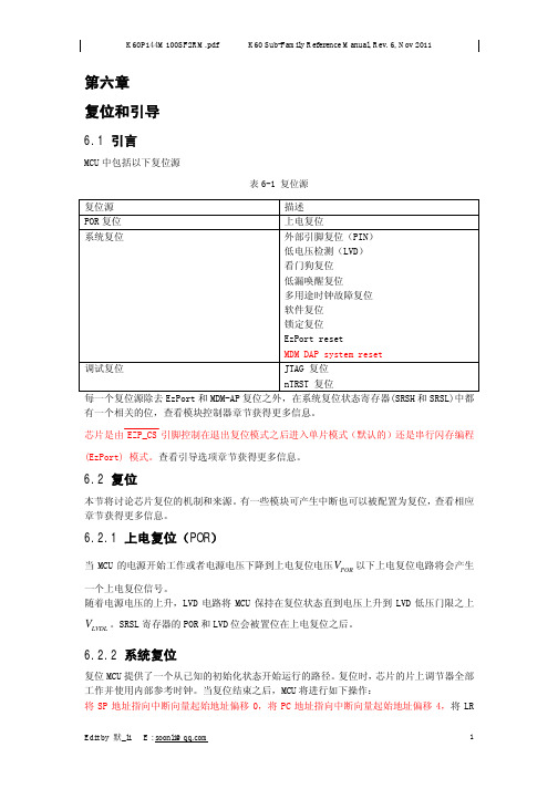
第六章复位和引导6.1 引言MCU中包括以下复位源表6-1 复位源复位源描述POR复位上电复位系统复位外部引脚复位(PIN)低电压检测(LVD)看门狗复位低漏唤醒复位多用途时钟故障复位软件复位锁定复位EzPort resetMDM DAP system reset调试复位JTAG 复位nTRST 复位每一个复位源除去EzPort和MDM-AP复位之外,在系统复位状态寄存器(SRSH和SRSL)中都有一个相关的位,查看模块控制器章节获得更多信息。
芯片是由EZP_CS引脚控制在退出复位模式之后进入单片模式(默认的)还是串行闪存编程(EzPort) 模式。
查看引导选项章节获得更多信息。
6.2 复位本节将讨论芯片复位的机制和来源。
有一些模块可产生中断也可以被配置为复位,查看相应章节获得更多信息。
6.2.1 上电复位(POR)V以下上电复位电路将会产生当MCU的电源开始工作或者电源电压下降到上电复位电压POR一个上电复位信号。
随着电源电压的上升,LVD电路将MCU保持在复位状态直到电压上升到LVD低压门限之上V。
SRSL寄存器的POR和LVD位会被置位在上电复位之后。
LVDL6.2.2 系统复位复位MCU提供了一个从已知的初始化状态开始运行的路径。
复位时,芯片的片上调节器全部工作并使用内部参考时钟。
当复位结束之后,MCU将进行如下操作:将SP地址指向中断向量起始地址偏移0,将PC地址指向中断向量起始地址偏移4,将LR设置为0xFFFF_FFFF。
片上所有外设模块全部禁止,所有的非模拟IO全部禁用。
模拟IO全部被设置为默认的模拟功能。
在复位过程和其结束之后,与JTAG相关的输入引脚被配置为:TDI输入被配置为上拉。
TCK输入被配置为下拉TMS被配置为上拉相关的输出引脚TDO配置无上拉也没有下拉。
注意nTRST引脚的初始化配置时禁用的。
但是一旦配置为JTAG功能之后他的功能将成为nTRST上拉。
6.2.2.1 外部复位引脚在器件中,复位引脚是一个专用的引脚,引脚是开漏的,有一个内部的上拉驱动,外部复位引脚可以将MCU从任何模式唤醒。
飞思卡尔K60入门资料课件

将JTAG调试器连接到计算 机,并下载和安装相应的 驱动程序。
打开Keil MDK-ARM软件 ,创建一个新项目,选择 正确的芯片型号(K60), 并配置项目属性,如工作 空间、工具链等。
使用串口通信线将开发板 与计算机连接起来,以便 在开发过程中进行调试和 数据传输。
使用Keil MDK-ARM软件 编写代码,并进行编译和 调试。
K60在图像处理中的应用
K60芯片具有高速的图像处理能力,可以用于实现各种图像处理算 法,如图像增强、目标检测、人脸识别等。
图像处理实例代码
提供一些基于K60芯片的图像处理实例代码,包括图像增强、目标 检测等。
通信系统实例
通信系统概述
通信系统是实现信息传输和交换的技术体系,包括无线通信、有 线通信、卫星通信等。
软件问题及解决方案
总结词
软件问题通常涉及到编程环境、编译错误、烧录程序等,需要检查软 件配置和代码错误。
编程环境配置
确保你使用的编程环境(如IAR Embedded Workbench、Keil uVision等)已正确配置,包括驱动程序安装、工具链设置等。
编译错误
检查代码是否有语法错误或逻辑错误,仔细阅读编译器给出的错误提 示,定位并修复问题。
K60在通信系统中的应用
K60芯片具有高速的通信接口和强大的数据处理能力,可以用于实 现各种通信系统,如无线通信网络、卫星通信系统等。
通信系统实例代码
提供一些基于K60芯片的通信系统实例代码,包括无线通信网络协 议栈的实现、卫星通信系统的数据处理等。
05
K60芯片常见问题及解决方案
硬件问题及解决方案
开发环境常见问题及解决方案
1. Keil MDK-ARM软件安装问题:确保从官方网 站下载正确的版本,并按照安装向导进行操作。 如果遇到问题,可以查阅Keil官方文档或寻求技 术支持。
K60功能介绍
一、超低功耗:1. 10 种带有功率和时脉闸控的低功耗模式,可优化外围设备活动和恢复时间。
停止电流<500 nA,运行电流<200 uA/MHz,停止模式唤醒时间4μs。
2. 完整内存,模拟运行可降至1.71V,令电池寿命延长。
3. 低漏电唤醒单元,可带有8 个内置模块和16 个引脚,作为低漏电停止(LLS)/超低漏电停止(VLLS) 模式的唤醒源。
4. 低功耗定时器支持在低功耗状态下系统的持续运行。
二、闪存、SRAM和FlexMemory5. 256 KB-1 MB闪存。
快速接入、高可靠性具备四级安全保护6. 64 KB-128 KB SRAM7. FlexMemory:32 字节- 16 KB 用户可分段的字节写入/清除EEPROM,适用于数据表/系统数据。
EEPROM 具有超过10M 的周期和70 μsec 写入时间的闪存(出现电力故障时不会发生数据丢失或损坏)。
没有用户或系统干预便可完成编程和清除功能,完全运行状态下可降至 1.71V。
此外,从256KB-512KB 的FlexNVM 还适用于额外编程代码、数据或EEPROM 备份三、混合信号功能:8. 多达四种可配置分辨率的高速16位ADC。
可采用单路或差分输出模式改善噪声抑制。
可编程延迟块触发功能转换时间可达500 ns9. 多达两个12位DAC可用于音频应用模拟波形生成10. 具有3 个高速比较器,通过将PWM 保持在安全状态,提供快速准确的电机过电流保护。
11. 多达四个64倍可编程增益放大器用于小型振幅信号转换12. 模拟基准电压为模拟块、ADC 和DAC 提供精确的基准值,可以替换外部基准电压,降低系统成本。
四、性能:13. ARM Cortex-M4 内核+ DSP。
100-180MHz、单周期MAC、单指令多数据(SIMD) 扩展、可选的单精度浮点单元。
14. 具有32 通道的DMA 适用于外围设备和内存,可降低CPU 负载,实现更快的系统吞吐量。
- 1、下载文档前请自行甄别文档内容的完整性,平台不提供额外的编辑、内容补充、找答案等附加服务。
- 2、"仅部分预览"的文档,不可在线预览部分如存在完整性等问题,可反馈申请退款(可完整预览的文档不适用该条件!)。
- 3、如文档侵犯您的权益,请联系客服反馈,我们会尽快为您处理(人工客服工作时间:9:00-18:30)。
14低功耗模式
14.1 简介
PMC包括内部电压调节器,上电复位(POR)以及低电压检测系统。
模式控制器控制PMC,本节主要的内容包含设备的所有复位。
14.2 特征
电源管理控制特征包括以下几个方面
(1)内部电压调节器;
(2)在检测到低电压时的有效上电复位;
(3)低电压检测保护,包括:多个可编程脱扣电压、警告和检测中断控制、在低电压检测时驱动复位。
14.3 低电压检测系统(LVD)
芯片包括一个防范低电压状态的系统,使芯片电压变化时能保护存储器内容并控制MCU的系统状态。
该系统是由一个上电复位(POR)电路和一个电压LVD电路组成的。
对于LVD电压,用户可选择脱扣电压有高(VLVDH)或低(VLVDL)两种。
脱扣电压由LVDSC1[LVDV]位决定。
进入VLPx,LLS和VLLSx模式时LVD被禁止。
有两个标志位可以用来指示低电压检测系统的状态:
(1)低电压检测标志(low voltage detect flag ,LVDF)在电平敏感的方式工作。
当内部供电低于选定的内部监控阈值(VLVD)时LVDF位被置1。
只有当内部供电回复到阈值电压之上时,才能通过LVDACK位写1才可将LVDF位清0。
否则,LVDF位保持为1。
(2)低电压警告标志(low voltage warning flag ,LVWF)在电平敏感的方式工作。
当内部供电低于选定的内部监控阈值(LVWF)时LVDF位被置1。
只有当内部供电回复到阈值电压之上时,才能通过LVDACK位写1才可将LVWF位清0。
否则,LVWF位保持为1。
14.3.1低电压复位操作
通过设置LVDRE位,检测到一个低电压状态后LVD产生一个复位。
低电压检测阈值取决于LVDV位。
在LVD复位后,LVD系统保持MCU的复位状态直到供电升高超过此阈值。
LVD或上电复位后SRS寄存器中的LVD位被置1。
14.3.2低电压中断操作
若需中断操作,则要配置LVD电路(LVDIE置1,LVDRE清0);LVDSC1[LVDF]置1并且当检测到一个低电压状态是就会产生一个LVD中断请求。
通过LVDSC1[LVDACK]位写1才可将LVDF位清0。
14.3.3低电压警告中断操作(Low-Voltage Warning ,LVW)
LVD系统包含一个低电压警告标志用以指示供电已经临近LVW电压但高于LVD电压。
LVW也有一个中断,LVDSC2[LVWIE]位置1可以使能中断请求。
若中断请求使能,则当LVWF置1时,一个LVW中断请求将产生。
通过向LVDSC2[LVWACK]位写1将LVWF
位清0。
LVDSC2[LVWV]位选定四个脱扣电压中的一个:最高(V LVW4)、两个中等(V LVW3和V LVW2)、最低(V LVW1)。
14. 4 PMC存储器映射/寄存器定义
14.4.1低电压检测状态与控制1寄存器(PMC_LVDSC1)
此寄存器包含状态与控制位以支持低电压检测功能。
此寄存器需在复位初始化程序时根据需要进行配置,即使之前写入的设置就是需要配置也要重新写一次。
当设备在超低电压或低功耗模式,无论LVDSC1怎样设置,LVD系统将被禁止。
为了保护系统,必须使得LVD总是启动,配置电源模式保护寄存器(power mode protection register ,PMPROT)以禁止任何超低电压或低功耗模式被使能。
参见设备芯片手册获取更详细的LVD信息。
注意:此寄存器的复位值取决于复位类型:
(1)POR — 0x10;(2)其他复位—4位置1,1-0位不受影响。
14.4.2低电压检测状态与控制2寄存器(PMC_LVDSC2)
此寄存器包含状态与控制位以支持低电压检测功能。
当设备在超低电压或低功耗模式,无论LVDSC2怎样设置,LVD系统将被禁止。
参见设备芯片手册获取更详细的LVD信息。
注意:LVW脱扣电压取决于LVWV和LVDV位。
注意:此寄存器的复位值取决于复位类型:(1)POR —0x00;(2)其他复位—1-0位不受影响。
地址:PMC_LVDSC2 –4007_D000h 基址+ 1h 偏移量= 4007_D001h
14.4.3调节器状态与控制寄存器(PMC_REGSC)
电压管理控制器包含一个内部电压调节器。
电压调节器用于带隙参考,同样可以用于一个缓存作为输入到指定的内部外设。
内部调节器提供一个状态位(REGONS)指示调节器处于运行调节状态。
当用于从低电压或超低电压,此时频率被限制于正常运行模式,跳出时可以使用。
应用的频率在调整器未处于运行调节状态((REGONS=1)时不能提高。
地址:PMC_REGSC –4007_D000h 基址+ 2h 偏移量= 4007_D002h。