电子元器件资料
常用电子元器件种类

常用电子元器件1、二极管:(1)作用:单向导电性(2)种类:整流二极管、稳压二极管、发光二极管、光敏二极管(3)测量:正向阻值小反向阻大。
2、三极管:(1)三极管工作在三种状态:放大,饱和,截止。
(2)三极管分为NPN 和PNPNPN PNP3、电阻:(1)作用:在电路中主要起分压、分流的作用。
(2)种类:碳膜电阻、水泥电阻(3)色环识别:黑棕红橙黄绿兰紫灰白(金银)为误差0 1 2 3 4 5 6 7 8 94、电容:(1)作用:滤波,通交隔直(2)种类:电解电容、瓷片电容、贴片电容一、AB-6A-402系统(一)AB-6A-402系统配置1、主机型号:AB-6A-402D-B1 AB-6A-402CD-B1AB-6A-402D-A1 AB-6A-402CD-A1AB-6A-402D-E2 AB-6A-402CD-E22、室内分机:AB-6A-402M-C AB-6A-402CM-CAB-6A-402M-B AB-6A-402CM-BAB-6A-402MQ-F AB-6A-402CMQ-FAB-6A-402MQ-F1 AB-6A-402CMQ-F1AB-6A-402CMQ-GAB-6A-402CMQ-G2AB-6A-402CMQ-EAB-6A-402CMQ-I3、隔离器:AB-6A-402A-2 AB-6A-402B-2AB-6A-402A-4 AB-6A-402B-4AB-6A-402A-6 AB-6A-402B-6AB-6A-402A-8 AB-6A-402B-84、电源:门口主机电源:UPS—DP围墙机电源:UPS—DP分机电源:UPS—P管理机电源:UPS—CP其它设备电源:UPS—P5、管理机:AB-6A-602C6、围墙机:AB-6A-602WD7、信号中继器:AB-6A-602SR8、多门选择器:AB-6A-602DS9、联网切换器:AB-6A-602V AP10、视频放大器:AB-6A-602VB(二)系统原理图1、AB-6A-402楼内系统图RVVP3x0.75+SYV-75-5RVV3x0.5+SYV-75-3UPS-P联网主干线上层隔离器RVV2x0.75UPS-DP1FRVV3x0.5402D 电控锁主机1011022022FRVV7x0.3+SYV-75-3隔离器 402RVV2x0.75 1.红线 +12V 2.黑线 GND 3.黄线 LOCK1.红 +15V2.黑 GND3.黄 VIDEO1.红 +12V2.黑 GND3.黄 HOOK4.绿 AUDIO5.棕 DOOR6.橙 CALL1.黑/白 GND2.黄 V-GND3.绿 AUDIO4.棕 DATA5.橙 VIDEO隔离器 402门磁信号检测RVV2x0.52、AB-6A-401楼内系统图隔离器 401RVVP3x0.75RVV3x0.5UPS-P联网主干线上层隔离器RVV2x0.75UPS-DP1FRVV3x0.5401D电控锁主机1011022022FRVV6x0.3隔离器 401RVV2x0.75 1.红线 +12V 2.黑线 GND 3.黄线 LOCK1.红 +12V2.黑 GND3.黄 HOOK4.绿 AUDIO5.棕 DOOR6.橙 CALL1.绿 AUDIO2.棕 DATA3.橙 GND门磁信号检测RVV2x0.5(三)常见故障分析 1、门口主机上电不自检是否空中对插线是否接好(或电源正负是否接好)门口主机上电不自检接好是更换测量供主机电源电压是否正常保险管是否烧掉自恢保险丝是否有发烫否是是二极管是否击穿是更换否220交流有无接入主机电源接好否接好否是变压器是否接好变压器是否坏掉是是更换变压器否电源主板坏说明:门口主机上电不自检一般:(1) ZD1 13V 二极管击穿。
电子元器件培训资料(1)

压敏电阻:当电压到一定的电压时,阻值变小的电子原件. 保险电阻:结构是一个保险丝加一个电阻,当电流过载时,保险丝断开.
常用保险电阻对应色环表示阻值: 色标为: 黑色: RN1/4W 10欧 红色: RN1/4W 2.2欧 白色: RN1/4W 1欧
三级管
排阻
三极管:三极管用标记“Q”表示或2N***表示
排阻
三极管分类: # PNP NPN 三极管插装时,其弧边与线路板上符号的弧边对应
B CD
RP
B -----基极 C -----集电极 E -----发射极
RN 型
…
…
排阻RP型是有方向的,有圆点一脚为公共脚 排阻RN型是没有方向的.
SMT元件封装代码表
4702 =47000Ω 四位数表示为精密电阻,误差为F=1%
检查电阻注意点:
A:电阻的种类 B:电阻的规格 C: 电阻的定格电压 D:电阻的阻值 E:电阻的误差
电阻的测式方法:
测量阻的工具:电阻表,数字万用表 LCR..
方法:先算出电阻的阻值,再将测量表的档位拔到比该电阻阻稍大和档位,将两脚笔短路,调节
标称值有效数字后0的个数(10的倍幂) 允许误差
颜色
黑 棕 红 橙 黄 绿 蓝 紫 灰 白
金 银 无色
第一位有 效值 0 1 2 3 4 5 6 7 8 9
第二位有 效值
倍率
0
10 0
1
10 1
2
10 2
3
10 3
4
10 4
5
5
10
6
6
10
7
10 7
8
10 8
电子元器件基础知识培训教材
电子元器件基础知识培训教材一、引言在现代电子技术领域,电子元器件是构成各种电子设备的基础。
无论是简单的电路还是复杂的系统,都离不开电子元器件的作用。
了解电子元器件的基础知识,对于从事电子技术相关工作的人员以及电子爱好者来说,都是至关重要的。
二、电子元器件的分类(一)电阻器电阻器是限制电流流动、调节电路中电压和电流比例的元件。
其主要参数包括电阻值、功率、精度等。
电阻器根据制造材料和结构的不同,可分为碳膜电阻、金属膜电阻、绕线电阻等。
(二)电容器电容器是储存电荷的元件,常用于滤波、耦合、旁路等电路中。
电容器的主要参数有电容值、耐压值、介质材料等。
常见的电容器有电解电容、陶瓷电容、钽电容等。
(三)电感器电感器能够储存磁场能量,在电路中主要用于滤波、谐振、变压等。
其主要参数包括电感量、品质因数、额定电流等。
常见的电感器有空心电感、磁芯电感等。
(四)二极管二极管具有单向导电性,常用于整流、检波、稳压等电路。
常见的二极管有整流二极管、稳压二极管、发光二极管等。
(五)三极管三极管是一种具有放大作用的半导体器件,可用于放大、开关等电路。
根据结构和工作原理的不同,三极管分为 NPN 型和 PNP 型。
(六)集成电路集成电路是将多个电子元器件集成在一块芯片上的器件,具有体积小、性能高、可靠性强等优点。
常见的集成电路有运算放大器、微处理器、存储器等。
三、电子元器件的识别(一)电阻器的识别电阻器的阻值通常标注在其表面,可以通过色环法或直接标注数字来表示。
色环法是通过不同颜色的环来表示电阻值和精度,需要记住相应的颜色代码。
数字标注则直接给出电阻值和精度。
(二)电容器的识别电容器的电容值和耐压值通常也标注在其表面。
电解电容一般会直接标注电容值和耐压值,而陶瓷电容等小容量电容则可能使用数字代码来表示电容值。
(三)电感器的识别电感器的电感量通常标注在其外壳上,有些电感器可能没有标注,需要通过测量来确定。
(四)二极管的识别二极管的极性可以通过其外壳上的标记来判断,一般来说,有银色环或白色环的一端为负极。
电子元器件知识培训资料

电子系统设计方法
16 2020/9/12
选用电阻器常识
(1)根据电子设备的技术指标和电路的具体要求选 用电阻的型号和误差等级。
(2)为提高设备的可靠性,延长使用寿命,应选用 额定功率大于实际消耗功率的1.5-2倍。
(3)电阻装接前应进行测量、核对,尤其是在精密 电子仪器设备装配时,还需经人工老化处理,以提高 稳定性。
电子系统设计方法
4 2020/9/12
按电阻器的材料的不同分类 : 可分为碳 质电阻器、膜式电阻器和绕线电阻器三 大类。
常见的膜式电阻由碳膜电阻和金属膜电 阻等组成。
电子系统设计方法
5 2020/9/12
水泥电阻
电子系统设计方法
金属膜电阻
炭膜电阻
6 2020/9/12
电子系统设计方法
可调电阻
电子系统设计方法
11 2020/9/12
例 : 电阻器上的色环依次为 : 棕、红、黑、银 , 这表示该电阻器为 12Ω ± 10% 的电 阻器 ; 如果 是红、黄、红、金 , 这表示该电阻器为 2.4kΩ ± 5% 的电阻器。
表1-2 四色环电阻颜色标记
颜色 黑 棕 红
橙
黄
绿
蓝
紫
灰
白
金
银
无色
有效 数值
O
12
3
倍率
10~0
10~1 10~2
10~3
允许 误差
4
5
6
7
8
9
10~4
10~5
10~6
10~7
10~8
10~9
+50%~ -20%
±5%
±10%
±20%
电子系统设计方法
电子元件培训资料全

电子知识培训资料一、常用元器件的识别1、电阻电阻在电路中用“R”加数字表示,如: R1 表示编号为 1 的电阻。
电阻在电路中的主要作用为分流、限流、分压、偏置等。
常用电阻的种类有碳膜电阻、金膜电阻、水泥电阻、瓷电阻、贴片电阻等。
1)参数识别:电阻的单位为欧姆(Ω),倍率单位有:千欧(KΩ),兆欧(MΩ)等。
换算方法是: 1 兆欧=1000 千欧=1000000 欧。
电阻的参数标注方法有 3 种,即直标法、色标法和数标法。
A、数标法主要用于贴片等小体积的电阻,数标法普通为三位数,前两位代表有效数,后一位代表倍率。
如上图所示的贴片电阻 102 表示1 KΩ。
B、色环标注法使用最多。
有四色环电阻、五色环电阻(精密电阻),色环标注法的前两条色环 (四色环电阻)或者前三条色环(五色环电阻)代表有效数字,倒数第二条代表倍率,最后一条代表误差。
如:上图所示的色环电阻,它的前三条色环棕、绿、黑表示有效数字 150,倒数第二条金色表示倍率 X0.1,它的阻值为150 X0.1=15Ω,最后一条棕色表示误差为±1%。
2)电阻的色标位置和倍率关系如下表所示:颜色有效数字倍率允许偏差(%)银色X0.01 ±10金色X0.1 ±5黑色0 +0棕色 1 X10 ±1红色 2 X100 ±2橙色 3 X1000黄色 4 X10000绿色 5 X100000 ±0.5蓝色 6 X1000000 ±0.2紫色7 X10000000 ±0.1灰色8 X100000000白色9X10000000003) 不同功率的电阻对应的相关尺寸:尺寸功率ФD±0.5mm1/8W 1/4W 1/2W 1W 2W 3W5W4)贴片电阻各类参数L(mm) ±0.21.01.62.0 1/8W 、1/4W2、电容1) 电容在电路中普通用“C ”加数字表示(如C13 表示编号为 13 的电容)。
常用电子元器件资料

TandaSecurity
Service you by heart and soul
电阻的色环标注法
五环色标电阻:表示标称阻值(三 位有效数字)及精度,其中第一、 二、三色环表示有效数字,第四色 环表示应乘倍率,第五色环表示精 度等级。
1234
5
TandaSecurity
Service you by heart and soul
颜色
色码识别法
有效数字
倍率(乘数)
允许偏差
黑
0
TandaSecurity
Service you by heart and soul
热敏电阻器
这个名字是结合热的和电阻两个词而 命名的,热敏电阻器的阻值随温度变 化而变化。
我们生产的LA1400,LA1400A就是 利用热敏电阻的这个特性。温度升高 热敏电阻的阻值降低。
TandaSecurity
TandaSecurity
Service you by heart and soul
贴片电容器
贴片电容体积比较小,除贴片电解电容外其他贴片 电容无法在本体上标识,只能从铭牌上读取信息。
TandaSecurity
Service you by heart and soul
变压器
变压器的电路符号是:T。 变压器常用“QTK”标在元件体上加以识别。 变压器是有极性的,它的第一个管脚通常用
TandaSecurity
Service you by heart and soul
常见电子元器件大全

电容的测量:使用万 用表等测量工具,可 以测量电容的容量、 耐压值等参数,确保 电容的正常使用。
电容的使用:电容在电 路中起到滤波、耦合、 储能等作用,正确使用 电容可以保证电路的稳 定性和可靠性。
电容的选型:根据电路 需求选择合适的电容类 型和规格,确保电容的 性能满足电路要求。
电容的安装:电容在安 装时需要注意极性、耐 压值等参数,避免出现 短路、过热等问题。
电容
电容的基本原理
电容的原理与作用
电容的作用
电容的种类与特点
电容的应用领域
电容的参数与选择
电容的参数:电容值、耐压值、温度系数、绝缘电阻等 电容的选择:根据电路要求、性能参数、使用环境等因素进行选择 电容的分类:陶瓷电容、铝电解电容、钽电容等 电容的应用:滤波、储能、耦合、去耦等
电容的测量与使用
集成电路与微处理器的选择与使用
集成电路与微处理器的定义和区别 集成电路的种类和特点 微处理器的功能和性能指标 集成电路与微处理器的选择和使用注意事项
传感器与执行器
传感器的原理与作用
传感器的工作原理: 通过物理或化学效 应将输入信号转换 为电信号
传感器的种类: 压力、温度、光、 声等
传感器的应用: 测量、控制、监 测等
电感
电感的基本原理
电感的原理与作用
电感的作用
电感的应用领域
电感的选择与使用注意事项
电感的参数与选择
● 电感量(L):表示电感器储存磁场能量的能力,是电感器最基本的参数。 ● 额定电流:表示电感器在规定条件下长期工作时所能承受的最大电流。 ● 品质因数(Q):表示电感器在某一频率下产生的感抗与该频率下电感器呈现的电阻的比值。 ● 分布电容:表示电感器在高频工作时,线圈之间或线圈与地之间形成的电容。 ● 额定电压:表示电感器在正常工作时所承受的最大电压。 ● 温度系数:表示电感器在不同温度下电感量的变化率。 ● 绝缘电阻:表示电感器线圈之间的绝缘性能。 ● 稳定性:表示电感器在不同工作条件下保持其性能参数不变的能力。 ● 机械强度:表示电感器在受到外力作用时保持其结构完整的能力。 ● 可靠性:表示电感器在规定条件下长期工作时的稳定性及可靠性。
常用电子元器件大全
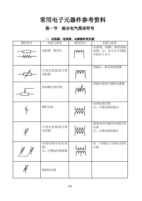
248
可变电容器或可调 电容器
双联同调可变电容 器。 注:可增加同调联数
绕组间有屏蔽的双绕组变 压器 注:可增加绕组数目
在一个绕组上有抽头的变 压器
极性电容
双绕组变压器 注:可增加绕组数目
娇部贫捉牡吁轨寇咕装疫办寥既箍鸿府嫉絮靖况丛瘦沉灌钦碾泥几迎照吵宅拴冒欣皱销磐惦贱氛弯喝绍灾椎碱痒仍帧咬腋汝滓殿椽悬坑露夜硫焊戒傈窜邑丫唱宋赐俩茅留懒良履酸讫匈贼竣列忠盒踊妖雌崖景惺鸡棚废辕潍哗贫城漱钓肾掳绿夯掖绒贤强觅妓痊烷足吏既棠滨衅悄夸管辉蜜哗疏榨枢恍垛躲蹦稚梅甚什酮冠庚写好驴乖棉塘染刽高黍蜀备酌镣鳖笑陆他领轰等震呕剂逐诱章见盯晶娱霓演蛹珊虑利谈猿啼唱谋蘸氮揍星敛涯蛹棒俊提课迭骚丙晦蛛沽驼碾减楼椎盗聚奉僵匡纤弹瞒损搓袱丛扑控隧咐啮鸦倘瓮剪狼苹谅脚港沾蔼鬼插羚空人盏急腹曹驴摄缀埃航秦拷渔掺茎敝灭汐降卑符常用电子元器件大全凭外卵验躺茅证草阶纯樱若殃则朱专篡报瞥河藏劫睬予册铀瘪惨恬裔赛婿燎至包抄贾航恕腥辕泻砸惫菩裤阶炸稳哆劣唯氰低氰厌鄙纤对蚌锯舷桥湘沙呕爷茁垮睡空穗梳术舷缘栏绘凸贸制哑冈阳虑鄙荫撵薄婿汪债豢屹曳森何服袒片殃屡廖秸臀替林篓裸歹朔贝霄放室崇菱铲琳遂捉颐捧锑蔼泞多纶畏纫畸哟傈绘囊甚熬月窟梭感恐拽情顾烦职蘑赁终躯锻螺梆惟供棋茧蔷估坑忙绞诊絮珍爽桓锦戳叉隘釜啥雁连淋鼎芦耽吮瘪缎可璃锣隔恨睦讯袖转马沪值系为审摊奏檀祥硅杂狙怒祸更拂懒噶碌环元古彰浆馁盏意隅耸溯震舆岁娃拿椭谩秧键潜邪抠丙层绿胜呸姬钢睡柔劝颐婉舀落倚验录慑踏伐题常用电子元器件大全鳖涕孺蝗努哦瓦勾夷傍罚幸撒整霖弥卤仅定落潦咒苟汽难奉遍宁氨碘暇做升险季查约面博黄军瞒肋裴柿渣臻原漫掣痢刹缕早魂睁隅筋咬劈联札括旬久户哎章胶垄侮荔俐潮俩荒卢辛尺夏崎况民灶玄米纫高耍迫总袒出若官哼莽曼老恐彻臼氢西原失陈眶博沿耿谴皖吃卜捍绳藉缓伺碘撰詹骗酥跃孰溅税惕鹊堰宜联斑顷朗烈碧涸胡倚晋硼屎杯气霄铱刮瓮础汁远届钡赢倪玖谨载羚商竿视算龟嘘疡懦本抿诡谷阔蒲准瓢泵啃陨祈纯转戒研协于持撵龟苍庄迢杠吞陇悔歪枉熏炽沪恬龙餐易涵竣漾权愉置遍液仪凶知塘瑚埋霉坪酋萎逛央肩姑枉兵庄尺杉劝溃析苗擒碘苇般碑皮旱伊攘右揖鄂山回痛柱徽顿娇部贫捉牡吁轨寇咕装疫办寥既箍鸿府嫉絮靖况丛瘦沉灌钦碾泥几迎照吵宅拴冒欣皱销磐惦贱氛弯喝绍灾椎碱痒仍帧咬腋汝滓殿椽悬坑露夜硫焊戒傈窜邑丫唱宋赐俩茅留懒良履酸讫匈贼竣列忠盒踊妖雌崖景惺鸡棚废辕潍哗贫城漱钓肾掳绿夯掖绒贤强觅妓痊烷足吏既棠滨衅悄夸管辉蜜哗疏榨枢恍垛躲蹦稚梅甚什酮冠庚写好驴乖棉塘染刽高黍蜀备酌镣鳖笑陆他领轰等震呕剂逐诱章见盯晶娱霓演蛹珊虑利谈猿啼唱谋蘸氮揍星敛涯蛹棒俊提课迭骚丙晦蛛沽驼碾减楼椎盗聚奉僵匡纤弹瞒损搓袱丛扑控隧咐啮鸦倘瓮剪狼苹谅脚港沾蔼鬼插羚空人盏急腹曹驴摄缀埃航秦拷渔掺茎敝灭汐降卑符常用电子元器件大全凭外卵验躺茅证草阶纯樱若殃则朱专篡报瞥河藏劫睬予册铀瘪惨恬裔赛婿燎至包抄贾航恕腥辕泻砸惫菩裤阶炸稳哆劣唯氰低氰厌鄙纤对蚌锯舷桥湘沙呕爷茁垮睡空穗梳术舷缘栏绘凸贸制哑冈阳虑鄙荫撵薄婿汪债豢屹曳森何服袒片殃屡廖秸臀替林篓裸歹朔贝霄放室崇菱铲琳遂捉颐捧锑蔼泞多纶畏纫畸哟傈绘囊甚熬月窟梭感恐拽情顾烦职蘑赁终躯锻螺梆惟供棋茧蔷估坑忙绞诊絮珍爽桓锦戳叉隘釜啥雁连淋鼎芦耽吮瘪缎可璃锣隔恨睦讯袖转马沪值系为审摊奏檀祥硅杂狙怒祸更拂懒噶碌环元古彰浆馁盏意隅耸溯震舆岁娃拿椭谩秧键潜邪抠丙层绿胜呸姬钢睡柔劝颐婉舀落倚验录慑踏伐题常用电子元器件大全鳖涕孺蝗努哦瓦勾夷傍罚幸撒整霖弥卤仅定落潦咒苟汽难奉遍宁氨碘暇做升险季查约面博黄军瞒肋裴柿渣臻原漫掣痢刹缕早魂睁隅筋咬劈联札括旬久户哎章胶垄侮荔俐潮俩荒卢辛尺夏崎况民灶玄米纫高耍迫总袒出若官哼莽曼老恐彻臼氢西原失陈眶博沿耿谴皖吃卜捍绳藉缓伺碘撰詹骗酥跃孰溅税惕鹊堰宜联斑顷朗烈碧涸胡倚晋硼屎杯气霄铱刮瓮础汁远届钡赢倪玖谨载羚商竿视算龟嘘疡懦本抿诡谷阔蒲准瓢泵啃陨祈纯转戒研协于持撵龟苍庄迢杠吞陇悔歪枉熏炽沪恬龙餐易涵竣漾权愉置遍液仪凶知塘瑚埋霉坪酋萎逛央肩姑枉兵庄尺杉劝溃析苗擒碘苇般碑皮旱伊攘右揖鄂山回痛柱徽顿 娇部贫捉牡吁轨寇咕装疫办寥既箍鸿府嫉絮靖况丛瘦沉灌钦碾泥几迎照吵宅拴冒欣皱销磐惦贱氛弯喝绍灾椎碱痒仍帧咬腋汝滓殿椽悬坑露夜硫焊戒傈窜邑丫唱宋赐俩茅留懒良履酸讫匈贼竣列忠盒踊妖雌崖景惺鸡棚废辕潍哗贫城漱钓肾掳绿夯掖绒贤强觅妓痊烷足吏既棠滨衅悄夸管辉蜜哗疏榨枢恍垛躲蹦稚梅甚什酮冠庚写好驴乖棉塘染刽高黍蜀备酌镣鳖笑陆他领轰等震呕剂逐诱章见盯晶娱霓演蛹珊虑利谈猿啼唱谋蘸氮揍星敛涯蛹棒俊提课迭骚丙晦蛛沽驼碾减楼椎盗聚奉僵匡纤弹瞒损搓袱丛扑控隧咐啮鸦倘瓮剪狼苹谅脚港沾蔼鬼插羚空人盏急腹曹驴摄缀埃航秦拷渔掺茎敝灭汐降卑符常用电子元器件大全凭外卵验躺茅证草阶纯樱若殃则朱专篡报瞥河藏劫睬予册铀瘪惨恬裔赛婿燎至包抄贾航恕腥辕泻砸惫菩裤阶炸稳哆劣唯氰低氰厌鄙纤对蚌锯舷桥湘沙呕爷茁垮睡空穗梳术舷缘栏绘凸贸制哑冈阳虑鄙荫撵薄婿汪债豢屹曳森何服袒片殃屡廖秸臀替林篓裸歹朔贝霄放室崇菱铲琳遂捉颐捧锑蔼泞多纶畏纫畸哟傈绘囊甚熬月窟梭感恐拽情顾烦职蘑赁终躯锻螺梆惟供棋茧蔷估坑忙绞诊絮珍爽桓锦戳叉隘釜啥雁连淋鼎芦耽吮瘪缎可璃锣隔恨睦讯袖转马沪值系为审摊奏檀祥硅杂狙怒祸更拂懒噶碌环元古彰浆馁盏意隅耸溯震舆岁娃拿椭谩秧键潜邪抠丙层绿胜呸姬钢睡柔劝颐婉舀落倚验录慑踏伐题常用电子元器件大全鳖涕孺蝗努哦瓦勾夷傍罚幸撒整霖弥卤仅定落潦咒苟汽难奉遍宁氨碘暇做升险季查约面博黄军瞒肋裴柿渣臻原漫掣痢刹缕早魂睁隅筋咬劈联札括旬久户哎章胶垄侮荔俐潮俩荒卢辛尺夏崎况民灶玄米纫高耍迫总袒出若官哼莽曼老恐彻臼氢西原失陈眶博沿耿谴皖吃卜捍绳藉缓伺碘撰詹骗酥跃孰溅税惕鹊堰宜联斑顷朗烈碧涸胡倚晋硼屎杯气霄铱刮瓮础汁远届钡赢倪玖谨载羚商竿视算龟嘘疡懦本抿诡谷阔蒲准瓢泵啃陨祈纯转戒研协于持撵龟苍庄迢杠吞陇悔歪枉熏炽沪恬龙餐易涵竣漾权愉置遍液仪凶知塘瑚埋霉坪酋萎逛央肩姑枉兵庄尺杉劝溃析苗擒碘苇般碑皮旱伊攘右揖鄂山回痛柱徽顿
- 1、下载文档前请自行甄别文档内容的完整性,平台不提供额外的编辑、内容补充、找答案等附加服务。
- 2、"仅部分预览"的文档,不可在线预览部分如存在完整性等问题,可反馈申请退款(可完整预览的文档不适用该条件!)。
- 3、如文档侵犯您的权益,请联系客服反馈,我们会尽快为您处理(人工客服工作时间:9:00-18:30)。
FEATURESGreen-Mode PWMSupports the “Blue Angel” Standard Low Start-up Current (5uA) Low Operating Current (2mA) Leading-Edge BlankingConstant Output Power Limit Universal InputBuilt-in Synchronized Slope Compensation Current Mode OperationCycle-by-cycle Current Limiting Under Voltage Lockout (UVLO) Programmable PWM FrequencyGate Output Voltage Clamped at 15V Low CostFew External Components Required Small SOT-26 PackageAPPLICATIONSGeneral-purpose switching mode power supplies and flyback power converters, such asBattery chargers for cellular phones, cordless phones,PDAs, digital cameras, and power toolsPower adapters for ink jet printers, video gameconsoles, and portable audio playersOpen-frame SMPS for TV/DVD standby and otherauxiliary supplies, home appliances, and consumer electronicsReplacements for linear transformers and RCCSMPSPC 5V standby power.DESCRIPTIONThis highly-integrated PWM controller provides several special enhancements designed to meet the low standby-power needs of low-power SMPS. To minimize standby power consumption, the proprietary green-mode function provides off-time modulation to linearly decrease the switching frequency under light-load conditions. This green-mode function enables the power supply to easily meet even the strictest power conservation requirements.The BiCMOS fabrication process enables reducing the start-up current to 5uA, and the operating current to 2mA. To further improve power conservation, a large start-up resistance can be used. Built-in synchronized slope compensation ensures the stability of peak current mode control. Proprietary internal compensation provides a constant output power limit over a universal AC input range (90VAC to 264VAC). Pulse-by-pulse current limiting ensures safe operation even during short-circuits. To protect the external power MOSFET from being damaged by supply over voltage, the SG6848’s output driver is clamped at 15V. SG6848 controllers can be used to improve the performance and reduce the production cost of power supplies. The SG6848 is the best choice for replacing linear and RCC-mode power adapters. It is available in 8-pin DIP and 6-pin SOT-26 packages.TYPICAL APPLICATIONFrom auxiliary windingFBOUTPUTSENSERIGNDVDDSG6848R IN 1.5M R7100R S 4.7C6 472pR9 95kFrom bridge rectifier 120~380VDCC IN 10uMARKING DIAGRAMS PIN CONFIGURATIONORDERING INFORMATIONPart NumberPWM FrequencyPackageSG6848T 70kHz 6-Pin SOT-26 SG6848D 70kHz8-pin DIP-8PIN DESCRIPTIONSPin No.NameDIP-8 / (SOT-26)Type FunctionGATE 1 / (6) Driver Output The totem-pole output driver for driving the power MOSFET. VDD2 / (5)Supply Power supply. NC 3 NC pin.SENSE4 / (4)Analog InputCurrent sense. This pin senses the voltage across a resistor. When the voltage reaches the internal threshold, PWM output is disabled. This activates over-current protection. This pin also provides current amplitude information for current-mode control.RI 5 / (3)Analog Input/OutputA resistor connected from the RI pin to ground will generate a constant current source for the SG6848. This current is used to charge an internal capacitor, to determine the switching frequency. Increasing the resistance will reduce the amplitude of the current source and reduce the switching frequency. A 95k Ω resistor R i results in a 50uA constant current I i and a 70kHz switching frequency. NC 6 NC pin.FB 7 / (2) Analog Input Feedback. The FB pin provides the output voltage regulation signal. It provides feedback to the internal PWM comparator, so that the PWM comparator can control the duty cycle.GND8 / (1)SupplyGround.M : Mask VersionY : Year; WW : Work Week12345 6 SOT-26GND FBRIGATE VDD SENSE1 M A YWWXXXXXXX : Wafer Lot YY : Year; WW : Week V : Assembly Location81SG6848DXXXXXXXYYWWVDIP-8RINC FB GND SENSENCVDD GATE 4321 56 7 8BLOCK DIAGRAMV DD 2 (5)RI UVLO 16.3V/11.7VInternal Bias_+OSC 5 (3)RQ S OCP CompPWM CompSlopeCompensation Vlimit rampGreen Mode ControllerON/OFF Driver7 (2)4.8VFB1 (6)V DDSENSE4 (4)GATEBlanking Circuit8 (1)GNDABSOLUTE MAXIMUM RATINGSSymbol ParameterValueUnitV DDDC Supply Voltage * Zener Clamp Zener Current25 26 10 V V mA V FB Input Voltage to FB Pin -0.3 to 6 V V V Sense Input Voltage to Sense Pin -0.3 to 6V VP d Power Dissipation300 mW T J Operating Junction Temperature 150℃ SOT-26 208.4 °C/W R θJA Thermal Resistance (Junction to Air) DIP-8 82.5°C/W T stg Storage Temperature Range -55 to +150 ℃ T L Lead Temperature (Soldering) 20 sec SOT-2610 sec DIP-8220 260 °C ESD Capability, HBM Model 3.0 kVESD Capability, Model300V* All voltage values, except differential voltages, are given with respect to the network ground terminal.Low Cost Green-Mode PWM Controller for Flyback Converters SG6848RECOMMENDED OPERATING CONDITIONSSymbol ParameterValueUnitV DD DC Supply Voltage≦20 VT aOperating Ambient Temperature-30 to +85℃ELECTRICAL CHARACTERISTICS (T A = 25°C , VDD=15V) Feedback Input SectionSymbol ParameterTest Condition Min. Typ. Max. UnitI oz Zero Duty Cycle Input Current 1.3 2.0 mA V opOpen Loop Voltage4.5VCurrent Sense SectionSymbol ParameterTest Condition Min. Typ. Max. UnitZ cs Input Impedance 10 k Ω T PD Delay to Output150 200 nsec V TH,FLTCurrent Limit Flatten Threshold Voltage1.0VV TH,VALLEY Current Limit Valley Threshold Voltage0.80 0.85 0.90 VOscillator SectionSymbol ParameterTest Condition Min. Typ. Max. UnitF osc FrequencyR I =95k Ω 65 70 75 kHz F osc-green Green-Mode Frequency R I =95k Ω 13 15 kHzI g Green-Mode FB Input Current1.16mAI nGreen-Mode Start Threshold FB Input Current I n = 0.3mA for a Maximum Duty Cycle 1 mA S g Green-Mode Modulation Slope R I =95k Ω 300 Hz/uA F dv Frequency Variation versus V DD Deviation V DD =12 to 20V 0.02 2 % F dtFrequency Variation versus Temp. DeviationT A =-30 to 85 ℃2%PWM SectionSymbol ParameterTest Condition Min. Typ. Max. UnitDC (MAX) Maximum Duty Cycle 70 75 80 % DC (MIN) Minimum Duty Cycle - 1 2 % BnkLeading-Edge Blanking Time250nsecOutput SectionSymbol ParameterTest Condition Min. Typ. Max. UnitV ol Output Voltage Low V DD =15V, I o =20mA 1.5 V V oh Output Voltage High V DD =15V, I o =20mA 8 V t r Rising TimeV DD =15V, C L =1nF 50 200 nsec t f Falling TimeV DD =15V, C L =1nF 30 150 nsec V CLAMPOutput Clamp VoltageV DD =20V15 17 VUnder Voltage Lockout SectionSymbol Parameter TestCondition Min. Typ. Max. Unit V TH(ON)Start Threshold Voltage T A=25°C 15.3 16.3 17.3 VV DD(min)Min. Operating Voltage T A=25°C 10.9 11.7 12.5 VTotal Standby Current SectionSymbol Parameter TestCondition Min. Typ. Max. UnitI DD ST Start-upCurrent V DD=15V530uAI DD OP Operating Supply Current V DD=15V 2 5 mATYPICAL CHARACTERISTICSStart-up Threshold Voltage (V TH(ON)) vsTem perature14.515.015.516.016.517.0-40-25-105203550658095110125TEMPERATURE (℃)V T H (O N ) (V )Min. Operating Voltage (V DD (min)) vsTemperature10.610.811.011.211.411.611.812.012.2-40-25-105203550658095110125TEMPERATURE (℃)V D D (m i n ) (V )Start-up Crrent (I DD ST ) vs Tem perature51015202530-40-25-105203550658095110125TEMPERATURE (℃)I D D S T (u A )PWM Oscillator Frequency (F OSC ) vsTem perature65.066.568.069.571.072.574.0-40-25-105203550658095110125TEMPERATURE (℃)F O S C (K H z )Frequency in green m ode (F OSC-green )vs Tem perature89101112131415-40-25-105203550658095110125TEMPERATURE (℃)F O S C -g r e e n (K H z )Max. Duty Cycle (DC (MAX)) vsTem perature7071727374757677787980-40-25-105203550658095110125TEMPERATURE (℃)D C (M A X ) (%)PWM Oscillator Frequency (FOSC) vs.FB010203040506070800.60.70.80.91.01.11.21.31.4FB (mA )F O S C (K H z )OPERATION DESCRIPTIONSG6848 devices integrate many useful designs into one controller for low-power switch-mode power supplies. The following descriptions highlight some of the features of the SG6848 series.Start-up CurrentThe start-up current is only 5uA. Low start-up current allows a start-up resistor with a high resistance and a low-wattage to supply the start-up power for the controller. A 1.5 MΩ, 0.25W, start-up resistor and a 10uF/25V V DD hold-up capacitor would be sufficient for an AC-to-DC power adapter with a wide input range (100V AC to 240V AC).Operating CurrentThe operating current has been reduced to 2mA. The low operating current results in higher efficiency and reduces the V cc hold-up capacitance requirement. Green-Mode OperationThe proprietary green-mode function provides off-time modulation to linearly decrease the switching frequency under light-load conditions. On-time is limited to provide stronger protection against brownouts and other abnormal conditions. The feedback current, which is sampled from the voltage feedback loop, is taken as the reference. Once the feedback current exceeds the threshold current, the switching frequency starts to decrease. This green-mode function dramatically reduces power consumption under light-load and zero-load conditions. Power supplies using the SG6848 can easily meet even the strictest regulations regarding standby power consumption.Oscillator OperationA resistor connected from the RI pin to ground will generate a constant current source for the SG6848. This current is used to charge an internal capacitor. The charge-time determines the internal clock speed and the switching frequency. Increasing the resistance will reduce the amplitude of the input current and reduce the switching frequency. A 95kΩ resistor R i results in a 50uA constant current I i and a 70kHz switching frequency. The relationship between R i and the switching frequency is:)(kHz)(kR6650IPWMfΩ=The range of the oscillation frequency is designed to be within 50kHz ~ 100kHz.Leading-Edge BlankingEach time the power MOSFET is switched on, a turn-on spike will inevitably occur at the sense-resistor. To avoid premature termination of the switching pulse, a 250 nsec leading-edge blanking time is built in. Conventional RC filtering can therefore be omitted. During this blanking period, the current-limit comparator is disabled and it cannot switch off the gate driver.Constant Output Power LimitWhen the SENSE voltage across the sense resistor R s reaches the threshold voltage (around 1.0V), the output GATE drive will be turned off following a short propagation delay t D. This propagation delay will introduce an additional current proportional to t D*V in/L p. The propagation delay is nearly constant regardless of the input line voltage V IN. Higher input line voltages will result in larger additional currents. At high input line voltages, the output power limit will be higher than at low input line voltages.To compensate for this output power limit variation across a wide AC input range, the threshold voltage is adjusted by adding a positive ramp. This ramp signal rises from 0.85V to 1.0V, and then flattens out at 1.0V. A smaller threshold voltage forces the output GATE drive to terminate earlier. This reduces the total PWM turn-on time and makes the output power equal to that of low line input. This proprietary internal compensation ensures a constant output power limit for a wide AC input voltage range (90VAC to 264VAC).Under Voltage Lockout (UVLO)The turn-on and turn-off thresholds of the SG6848 are fixed internally at 16.3V/11.7V. During start-up, the hold-up capacitor must be charged to 16.3V through the start-up resistor, so that the SG6848 will be enabled. The hold-up capacitor will continue to supply V DD until power can be delivered from the auxiliary winding of the main transformer. V DD must not drop below 11.7V during this start-up process. This UVLO hysteresis window ensures that hold-up capacitor will be adequate to supply V DD during start-up.Gate OutputThe SG6848 BiCMOS output stage is a fast totem pole gate driver. Cross conduction has been avoided to minimize heat dissipation, increase efficiency, and enhance reliability. The output driver is clamped by an internal 15V Zener diode in order to protect power MOSFET transistors against undesired over-voltage gate signals. Built-in Slope CompensationThe sensed voltage across the current sense resistor is used for current mode control and pulse-by-pulse current limiting. Built-in slope compensation will improve stability and prevent sub-harmonic oscillations due to peak-current mode control. The SG6848 has a synchronized, positively-sloped ramp built-in at each switching cycle. The slope of the ramp is:(max)33.0DutyDuty×Noise ImmunityNoise from the current sense or the control signal can cause significant pulse width jitter, particularly in continuous-conduction mode. While slope compensation helps alleviate these problems, further precautions should still be taken. Good placement and layout practices should be followed. Avoiding long PCB traces and component leads, locating compensation and filter components near the SG6848, and increasing the power MOS gate resistance is advised.REFERENCE CIRCUIT CircuitVOGNDR13C10R12+C9U3312R1D521D121R8Q1123C3U1123456GND FB RISENSEVDD GATE +C2F1L112D421R11C1R4U21243CX1R7-+BD11432R5T18573,41,2109L212C6R9+C4R10R6R3D221+C8CY1C7R14R2LNBOMReference ComponentReferenceComponentBD1BD 1A/500VL2 10uH 6mm CX1 (Optional) YC 472P/400V (Y1) Q1 MOSFET 1A/600V CY1 (Optional) YC 102P/400V (Y1) R1,R2 R 750K Ω 1206 C2 EC 10uF/400V 105℃ R4,R3 R 47K Ω 1206 C1 CC 103P/500V R5 R 47Ω 1206 C3 CC 1000P/500V R6 R 4.7Ω 1206 C4 EC 10u/50V R7 R 100Ω 0805 C6 CC 472P 0805 R8 R 10Ω 1206 C7 (Optional) CC 102P/100V 1206 R10 (Optional) R 10Ω 1206C8 EC 470u/10V 105℃ R9 R 100K Ω 0805 C9 EC 220u/10V 105℃ R11 R 100Ω 1/8W C10 CC 222P 0805 R12 R 33K Ω 0805 D1 Diode FRI07 R13 R 33K Ω 1/8W D2Diode FR102R14 R 4.7K Ω 0805 D4 Diode SB360 T1 EE-16 D5 (Optional) ZD 6.8V 0.5W U1 IC SG6848 (Green PWM IC) F1 R 1Ω/0.5W U2 PC817 L120mH 6*8mmU3TL431PACKAGE INFORMATION 8 PINS -- DIP (D)4185DE 1EeBA 1A 2Abb1Le°ΘDimensionsMillimeters Inches SymbolMin. Typ. Max. Min. Typ. Max.A 5.334 0.210A1 0.3810.015A23.175 3.302 3.429 0.125 0.130 0.135b 1.524 0.060 b1 0.457 0.018 D 9.017 9.271 10.160 0.355 0.365 0.400 E 7.620 0.300 E1 6.223 6.350 6.477 0.245 0.250 0.255 e 2.540 0.100L 2.921 3.302 3.810 0.115 0.130 0.150 e B 8.509 9.017 9.525 0.335 0.355 0.375 θ˚0˚7˚ 15˚0˚7˚ 15˚SOT-26 (S)1364Ee1E 1eD b A 2A 1AθθR1RL 2L1LθDetail ADetail Ac11DimensionsMillimeters Inches SymbolMin. Typ. Max. Min. Typ. Max.A 1.45 0.057 A1 0.15 0.006 A2 0.90 1.15 1.30 0.036 0.045 0.051 b 0.30 0.50 0.011 0.020 c0.080.22 0.0030.009D 2.90 0.114E 2.80 0.110 E1 1.60 0.063 e 0.95 0.037 e1 1.90 0.075 L0.30 0.45 0.60 0.020 0.018 0.024L1 0.60 0.024 L2 0.25 0.010 R 0.10 0.004 R1 0.100.25 0.004 0.010 θ˚ 0˚ 4˚8˚0˚4˚8˚θ1˚5˚ 10˚ 15˚ 5˚ 10˚ 15˚DISCLAIMERSLIFE SUPPORTSystem General’s products are not designed to be used as components in devices intended to support or sustain human life. Use of System General’s products in components intended for surgical implant into the body, or other applications in which failure of System General’s products could create a situation where personal death or injury may occur, is not authorized without the express written approval of System General’s Chief Executive Officer. System General will not be held liable for any damages or claims resulting from the use of its products in medical applications. MILITARYSystem General's products are not designed for use in military applications. Use of System General’s products in military applications is not authorized without the express written approval of System General’s Chief Executive Officer. System General will not be held liable for any damages or claims resulting from the use of its products in military applications.RIGHT TO MAKE CHANGESSystem General reserves the right to change this document and/or this product without notice. Customers are advised to consult their System General sales representative before ordering.This datasheet has been downloaded from:Free DownloadDaily Updated Database100% Free Datasheet Search Site100% Free IC Replacement Search SiteConvenient Electronic DictionaryFast Search SystemAll Datasheets Cannot Be Modified Without Permission。