奇晶飞升PCB800182产品中文规格书
FPGA可编程逻辑器件芯片XCKU085-2FLVA1517E中文规格书
Board InstallationIntroductionThis appendix provides the information required to install, program, debug, and deploy a Xilinx® accelerator board to execute applications created with the SDx® environment. The SDx environment executes in hardware using one of the FPGA boards listed in the application.Installing a BoardThe KCU1500 card is a high-performance reconfigurable computing card for data center applications and includes these features:•XCKU1500-2FLVB2104E FPGA •Four 4GB DDR4 banks (16GB total)The following sections describe how to install a board.Step 1: Set Up the Card and Computer1.Make sure the host computer is completely turned off.2.Install the FPGA board in an open PCIe® slot on the host computer.3.Turn on the host computer.Note:Follow the host computer manufacturer recommendations to ensure proper mountingand adequate cooling.找FPGA 和CPLD 可编程逻辑器件,上赛灵思半导体(深圳)有限公司Step 2: Prepare Board Installation FilesThe SDx environment provides the xbinst utility, which generates firmware and driver files for the target board plugged into the deployment computer.1.Run the following commands to prepare files for the target board installation.See the SDx Command and Utility Reference Guide (UG1279) [Ref6] for more details on the xbinst utility. Depending on the target location, some commands must be run with root or sudo privilege. Otherwise, access permissions must be changed to enable read access for all users on that system.e the following commands to create the deployment area inside/opt/dsa/:$ mkdir /opt/dsa$ mkdir /opt/dsa/xilinx_vcu1525_dynamic_5_1$ cd /opt/dsa/xilinx_vcu1525_dynamic_5_1Note:To install and deploy the KCU1500 files, use xilinx_kcu1500_dynamic_5_0 in step 2 and 3.3.Execute xbinst to install the files needed for the deployment machine. Output similarto the following is displayed:$ xbinst --platform xilinx_vcu1525_dynamic_5_1 -d .****** xbinst v2018.2 (64-bit)**** SW Build 2254440 on Sun Jun 10 18:05:35 MDT 2018** Copyright 1986-2018 Xilinx, Inc. All Rights Reserved.Attempting to get a license: ap_openclFeature available: ap_openclINFO: [XBINST 60-895] Target platform:/opt/Xilinx/SDx/2018.2/platforms/xilinx_vcu1525_dynamic_5_1/xilinx_vcu1525_dynamic_ 5_1.xpfmINFO: [XBINST 60-267] Packaging for PCIe...INFO: [XBINST 60-1032] Extracting DSA to./.Xil/xbinst-1273/xilinx_vcu1525_dynamic_5_1INFO: Adding section [FIRMWARE (3)] using: 'mgmt' (23192 Bytes)INFO: Adding section [SCHED_FIRMWARE (5)] using: 'sched' (9748 Bytes)Successfully completed 'xclbincat'INFO: [XBINST 60-268] Packaging for PLETEINFO: [XBINST 60-667] xbinst has successfully created a board installation directory at /opt/dsa/xilinx_vcu1525_dynamic_5_1.The files are installed in this location:/opt/dsa/xilinx_vcu1525_dynamic_5_1/xbinst:Make a note of the deployment location area because it is required at a later stage.This section refers to this location as the <xbinst-area> or as the deploymentdirectory.4.Install the drivers as described in Step 3: Install Board Drivers.Capabilities: <access denied>Kernel driver in use: xoclKernel modules: xocl03:00.1 Serial controller: Xilinx Corporation Device 6a8f (prog-if 01 [16450]) Subsystem: Xilinx Corporation Device 4351Control: I/O+ Mem+ BusMaster- SpecCycle- MemWINV- VGASnoop- ParErr- Stepping- SERR- FastB2B- DisINTx-Status: Cap+ 66MHz- UDF- FastB2B- ParErr- DEVSEL=fast >TAbort- <TAbort- <MAbort- >SERR- <PERR- INTx-Region 0: Memory at f4000000 (32-bit, non-prefetchable) [size=32M]Region 2: Memory at f8020000 (32-bit, non-prefetchable) [size=128K]Region 4: Memory at f8000000 (32-bit, non-prefetchable) [size=128K]Capabilities: <access denied>Kernel driver in use: xclmgmtKernel modules: xclmgmt。
ASUS ExpertCenter D7 Tower 商品说明书

Secure, reliable, andbusiness-readyEngineered to be powerful, tough, secure for business, ASUS ExpertCenter D7 Tower is powered by cutting-edge processors, fast memory and high-performance graphics. It meets MIL-STD-810G US military standards and features advanced security solutions.ProductivityGet what you need done, quickly and efficiently Effortless performanceTo make light work of all your business tasks, ExpertCenter D7 Tower is powered by cutting-edge 10th Gen Intel® Core™ processors with the latest DDR4 RAM. Up to three displays can be used simultaneously without adding an extra graphics card. Elevate your craft with NVIDIA graphicsExpertCenter D7 Tower is available with professional-grade NVIDIA® Quadro® and GeForce® graphics, certified by Independent Software Vendor (ISV) certification processes. Comprehensive connectionsFlexible serial and parallel ports on chassis leave more PCI slots available for additional upgrades. A smart-card reader and an SD card reader are optional for an easy transaction, data transfer, or other business-related tasks.Expandability and durabilityMeet your business now and in the futureUS Military gradeExpert series PCs are solidly built and engineered to meet strict military-grade MIL-STD 810G durability standards, so it’s ready to help your business for years to come.World’s #1 motherboardsExpertCenter desktops use ASUS motherboards — the world’s #1 motherboards1 — which are renowned for offering comprehensive system protection to safeguard hardware and 24/7 stability.100% solid capacitorsASUS uses only solid capacitors, which are more stable, tolerate higher ripple current, and generate less heat than standard electrolytic capacitors.D7 Tower | D700TASPECIFICATIONS | 1. ASUS secured the #1 spot for motherboard market share as of 2017, with DigiTimes reporting that the Taiwanese PC component giant owns 45% of the motherboard market.2. Kensington security slot and Padlock slot built in chassis ; Chassis Intrusion is optional.3. ASUS Business Manager includes Security Drive, Security Flash, Security Guard, File Shredder, System Backtrack, and My Logo.4. EPEAT country list please refer to: /.5. All accessories may vary in different market. Brand and product names mentioned are trademarks of their respective companies.6. Product specifications may differ from country to country. We recommend that you check with your local dealers for the specifications of the products available in your country.7. Colors of products may not be perfectly accurate due to variations caused by photography and monitor settings.8. Although we endeavor to present the most accurate and comprehensive information at the time of publication, we reserve the right to make changes without prior notice.D700TAASUS Back I/O Protector Asus 27" Eye Care Monitor (VP279N)ASUS Parallel Port Cable ASUS 27” Business Monitor (BE279CLB)ASUS Serial Port Extension CardHyper-Fast Networking (XG-U2008)RECOMMENDED ACCESSORIESUSB 3.2 Gen 1 port + USB-C™ port or USB 3.2 Gen 1 port x 2Optical disk driver bay (optional)HDD indicator Microphone port Headhone port USB 2.0 port x 2Smart card reader & SD card reader (optional)Serial port (optional)Parallel port (optional)PS/2 Mouse port PS/2 Keyboard portDisplayPort x 2HDMI port USB 3.2 Gen 1 port x 4USB 2.0 port x 2VGA portLAN (RJ-45) port Microphone portLine out port Line in portOMNI-CONNECTIVITYMultiple connections ensuring a seamless interface。
仪表芯片资料

符号 VDD(VDDA)—VSS(VSSA)
Tstg Temp Time
定额 -0.2V~4V -0.3V~VDD +0.3V
±2mA -50℃~+ 150℃
300℃ 10 秒
500mW
8.2 推荐工作条件
符号Βιβλιοθήκη 参数VDD电源电压
VSS
电源电压
时钟晶振
XT
外振荡 频率
陶瓷振荡器
石英晶振
测试条条件 所有外围组件及 CPU
17
PT1.7,PSDO,BZ
I/O, O
数 据 输 入 / 输 出 口 , 蜂 鸣 器 输 出 ,OTP 读 / 写 接 口 (PSDO)。
18
PT1.6,SCK
I/O 数据输入/输出口,SPI 通讯输出接口(SCK)。
19
PT1.5,SDO
I/O, O 数据输入/输出口,SPI 通讯输出接口(SDO)。
20
PT1.4,TX
I/O, O 数据输入/输出口,EUART 通讯接口(TX)。
21
PT1.3,RC,TST
I
数据输入口, EUART 通讯接口(RC) ,测验模式致能。
22
PT1.2,SDI
I/O, I 数据输入/输出口,SPI 通讯接口(SDI)。
23
PT1.1 SCE,PSDI,INTI
I/O I
PDF 文件使用 "pdfFactory Pro" 试用版本创建
Dream Tech International
4 应用领域
4.1 自动量程/手动量程掌上型数字多用表。 4.2 自动量程/手动量程名片型数字多用表。 4.3 自动量程笔式数字多用表。 4.4 自动量程钳型表。 4.5 数字面板表。
FPGA可编程逻辑器件芯片XCKU11P-2FFVE1517E中文规格书

SummaryThe Xilinx ® Kintex ® UltraScale+™ FPGAs are available in -3, -2, -1 speed grades, with -3E devices having the highest performance. The -2LE and -1LI devices can operate at a V CCINT voltage at 0.85V or 0.72V and provide lower maximum static power. When operated at V CCINT = 0.85V, using -2LE and -1LI devices, the speedspecification for the L devices is the same as the -2I or -1I speed grades. When operated at V CCINT = 0.72V, the -2LE and -1LI performance and static and dynamic power is reduced.DC and AC characteristics are specified in extended (E), industrial (I), and military (M) temperature ranges.Except the operating temperature range or unless otherwise noted, all the DC and AC electrical parameters are the same for a particular speed grade (that is, the timing characteristics of a -1 speed grade extended device are the same as for a -1 speed grade industrial device). However, only selected speed grades and/or devices are available in each temperature range.The XQ references in this data sheet are specific to the devices available in XQ Ruggedized packages. See the Defense-Grade UltraScale Architecture Data Sheet: Overview (DS895) for further information on XQ Defense-grade part numbers, packages, and ordering information.All supply voltage and junction temperature specifications are representative of worst-case conditions. The parameters included are common to popular designs and typical applications.This data sheet, part of an overall set of documentation on the Kintex UltraScale+ FPGAs, is available on the Xilinx.DC CharacteristicsAbsolute Maximum RatingsKintex UltraScale+ FPGAs Data Sheet:DC and AC Switching CharacteristicsTable 12: Differential SelectIO DC Input and Output LevelsI/O StandardV ICM (V)1V ID (V)2V ILHS3V IHHS3V OCM (V)4V OD (V)5 Min Typ Max Min Typ Max Min Max Min Typ Max Min Typ MaxSUB_LVDS80.5000.900 1.3000.070––––0.7000.900 1.1000.1000.1500.200 LVPECL0.300 1.200 1.4250.1000.3500.600––––––––SLVS_400_180.0700.2000.3300.140–0.450––––––––SLVS_400_250.0700.2000.3300.140–0.450––––––––MIPI_DPHY_DCI_HS90.070–0.3300.070–––0.0400.4600.1500.2000.2500.1400.2000.270Table 27: Maximum Physical Interface (PHY) Rate for Memory InterfacesMemoryStandard Packages DRAM Type Speed Grade and V CCINT Operating VoltagesUnits 0.90V0.85V0.72V-3-2-1-2-1DDR4All FFV and FFRpackages Single rank component26662666240024002133Mb/s1 rank DIMM1, 2, 324002400213321331866Mb/s2 rank DIMM1, 421332133186618661600Mb/s 4 rank DIMM1, 51600160013331333N/A Mb/sSFVB784 and SFRB784Single rank component24002400213321331866Mb/s1 rank DIMM1, 221332133186618661600Mb/s2 rank DIMM1, 418661866160016001600Mb/sTable 27: Maximum Physical Interface (PHY) Rate for Memory Interfaces (cont'd)MemoryStandard Packages DRAM Type Speed Grade and V CCINT Operating VoltagesUnits 0.90V0.85V0.72V-3-2-1-2-1DDR3All FFV and FFRpackages Single rank component21332133213321331866Mb/s1 rank DIMM1, 218661866186618661600Mb/s2 rank DIMM1, 416001600160016001333Mb/s 4 rank DIMM1, 51066106610661066800Mb/sSFVB784 and SFRB784Single rank component18661866186618661600Mb/s1 rank DIMM1, 216001600160016001600Mb/s2 rank DIMM1, 416001600160016001333Mb/s4 rank DIMM1, 51066106610661066800Mb/sDDR3L All FFV and FFRpackages Single rank component18661866186618661600Mb/s1 rank DIMM1, 216001600160016001333Mb/s2 rank DIMM1, 413331333133313331066Mb/s 4 rank DIMM1, 5800800800800606Mb/sSFVB784 and SFRB784Single rank component16001600160016001600Mb/s1 rank DIMM1, 216001600160016001333Mb/s2 rank DIMM1, 413331333133313331066Mb/s4 rank DIMM1, 5800800800800606Mb/s QDR II+All Single rank component6633633600600550MHz RLDRAM 3All FFV and FFRpackagesSingle rank component1200120010661066933MHz SFVB784 and SFRB784Single rank component10661066933933800MHz QDR IV XP All Single rank component106610661066933933MHz LPDDR3All Single rank component16001600160016001600Mb/s Notes:1.Dual in-line memory module (DIMM) includes RDIMM, SODIMM, UDIMM, and LRDIMM.2.Includes: 1 rank 1 slot, DDP 2 rank, LRDIMM 2 or 4 rank 1 slot.3.For the DDR4 DDP components at -3 and -2 (V CCINT = 0.85V) speed grades, the maximum data rate is 2133 Mb/s for six or more DDPdevices. For five or less DDP devices, use the single rank DIMM data rates for the -3 and -2 (V CCINT = 0.85V) speed grades.4.Includes: 2 rank 1 slot, 1 rank 2 slot, LRDIMM 2 rank 2 slot.5.Includes: 2 rank 2 slot, 4 rank 1 slot.6.The QDRII+ performance specifications are for burst-length 4 (BL = 4) implementations.FPGA Logic Switching CharacteristicsThe following IOB high-density (HD) and IOB high-performance (HP) tables summarize the values of standard-specific data input delay adjustments, output delays terminating at pads (based on standard) and 3-state delays.•T INBUF_DELAY_PAD_I is the delay from IOB pad through the input buffer to the I-pin of an IOB pad. The delay varies depending on the capability of the SelectIO input buffer.•T OUTBUF_DELAY_O_PAD is the delay from the O pin to the IOB pad through the output buffer of an IOB pad.The delay varies depending on the capability of the SelectIO output buffer.Table 29: IOB High Performance (HP) Switching Characteristics (cont'd)I/O StandardsT INBUF_DELAY_PAD_I T OUTBUF_DELAY_O_PAD T OUTBUF_DELAY_TD_PADUnits 0.90V0.85V0.72V0.90V0.85V0.72V0.90V0.85V0.72V-3-2-1-2-1-3-2-1-2-1-3-2-1-2-1SSTL15_DCI_S0.3190.4020.4170.4020.4170.7680.7680.8220.7680.8220.8470.8470.9120.8470.912ns SSTL15_F0.3200.3710.4000.3710.4000.3930.4080.4280.4080.4280.4940.5300.5560.5300.556ns SSTL15_M0.3200.3710.4000.3710.4000.5470.5540.5850.5540.5850.6240.6390.6770.6390.677ns SSTL15_S0.3200.3710.4000.3710.4000.7670.7670.8170.7670.8170.8130.8130.8670.8130.867ns SSTL18_I_DCI_F0.2560.3290.3360.3290.3360.4220.4450.4610.4450.4610.5400.5660.5950.5660.595ns SSTL18_I_DCI_M0.2560.3290.3360.3290.3360.5520.5540.5850.5540.5850.6290.6440.6830.6440.683ns SSTL18_I_DCI_S0.2560.3290.3360.3290.3360.7620.7620.8180.7620.8180.8370.8370.8990.8370.899ns SSTL18_I_F0.2590.3160.3370.3160.3370.4390.4540.4760.4540.4760.5490.5780.6080.5780.608ns SSTL18_I_M0.2590.3160.3370.3160.3370.5670.5710.6030.5710.6030.5350.6520.6920.6520.692ns SSTL18_I_S0.2590.3160.3370.3160.3370.7820.7820.8350.7820.8350.8160.8160.8700.8160.870ns SUB_LVDS0.5080.5390.6200.5390.6200.6580.6600.6920.6600.692907.4969.863nsSymbol Description Speed Grade and V CCINT Operating VoltagesUnits 0.90V0.85V0.72V-3-2-1-2-1T OUTBUF_DELAY_TE_PAD T input to pad high-impedance for HD I/Obanks6.167 6.318 6.369 6.699 6.752nsT input to pad high-impedance for HP I/Obanks5.330 5.330 5.341 5.330 5.341nsT INBUF_DELAY_IBUFDIS_O IBUF turn-on time from IBUFDISABLE to Ooutput for HD I/O banks2.266 2.266 2.430 2.266 2.430nsIBUF turn-on time from IBUFDISABLE to Ooutput for HP I/O banks0.8730.936 1.0370.936 1.037ns。
1.8寸LCD模块用户手册说明书
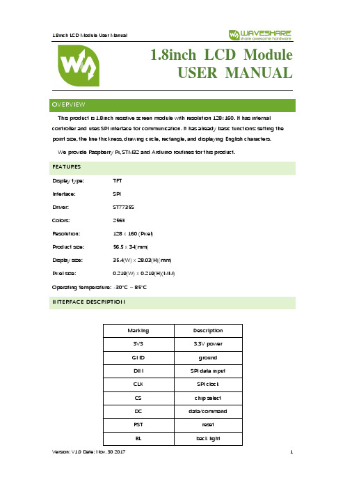
1.8inch LCD ModuleUSER MANUALOVERVIEWThis product is 1.8inch resistive screen module with resolution 128x160. It has internal controller and uses SPI interface for communication. It has already basic functions: setting the point size, the line thickness, drawing circle, rectangle, and displaying English characters.We provide Raspberry Pi, STM32 and Arduino routines for this product.FEATURESDisplay type: TFTInterface: SPIDriver: ST7735SColors: 256KResolution: 128 x 160 (Pixel)Product size: 56.5 x 34(mm)Display size: 35.4(W) x 28.03(H)(mm)Pixel size: 0.219(W) x 0.219(H)(MM)Operating temperature: -30°C ~ 85°CINTERFACE DESCRIPTIONMarking Description3V3 3.3V powerGND groundDIN SPI data inputCLK SPI clockCS chip selectDC data/commandRST resetBL back lightPROGRAM ANALYSIS1.Working principles:ST7735S is 132 x 162 pixels LCD panel, but the product is 128 x 160 pixels LCD display.In the display there are two processes: the horizontal direction scanning – from the 2nd pixel, the vertical direction scanning – from the 1st pixel. So, you can see that positions of pixels in RAM correspond to their actual positions while displaying.The LCD supports 12-bit, 16-bit and 18-bit per pixel input formats. They correspond to RGB444, RGB565 and RGB666 color formats. This routine uses the RGB565 color format, which is commonly used.LCD uses 4-wired SPI communication interface, which can save a lot of GPIO ports and provides fast data transfer to LCD as well.munication protocolNote: there is a difference from traditional SPI. Here we only need display, so sine wires come from slave to host are hidden. The detailed information please refer to datasheet at page 58RESX: Reset. Pull-down while powering on the module. Generally set as 1IM2: data communication mode pin, which define usage of SPICSX: chip selection control pin. If CS=0 – the chip is selectedD/CX: data/command control pin, if DC=0 – command is written, otherwise – data are writtenSDA: transmitted RGB dataSCL: SPI clockThe SPI communication protocol of the data transmission uses control bits: clock phase (CPHA) and clock polarity (CPOL):The value of CPOL determines the level when the serial synchronous clock is in idle state. CPOL=0, that its idle level is 0.The value of CPHA determines the timing of the data bits relative to the clock pulses. CPHA=0, data is sampled at the first clock pulse edge.The combination of these two parameters provides 4 modes of SPI data transmission. The commonly used is SPI0 mode, it is that GPOL=0 and CPHA=0.From the figure above, SCLK begins to transfer data at the first falling edge. 8 bits data are transferred at one clock period. Use SPI0 mode, High bits transfer first, and LOW bits following. DEMO CODERaspberry Pi, STM32 and Arduino programs are provided, wherein Raspberry Pi provides BCM2835, WiringPi and python programs. It implements common graphical functions as drawing dot, line, rectangle, circle, setting their sizes and line with; filling arias, and displaying English characters of 5 common fonts and other display’s functions.Following instructions are offered for you convenienceRASPBERRY1.Hardware connection1.8inch LCD module Raspberry Pi3.3V 3.3VGND GNDDIN MOSI (PIN 19)CLK SCLK (PIN23)CS CE0 (PIN 8)DC GPIO.6 (PIN 22)RST GPIO.2 (PIN13)BL GPIO.5 (PIN18)2.Enable SPI function of the Raspberry Pisudo raspi-configSelect: Advanced Options -> SPI -> yesActivate SPI hardware driver.3.Installation of librariesFore detailed information about libraries installation, please refer to this page:https:///wiki/Libraries_Installation_for_RPiIt is description of WiringPi, bcm2835 and python libraries installation.ageBCM2835 and WiringPi program should be only copied into directory of Raspberry Pi ()by samba or directly copy to the SD card). The following code are compied directly to the user directory of Pi.4.1Usage of BCM2835Run ls command as you can see below:bin: contains “.o” files.We don’t need to change it generallyFonts: contains 5 commonly used fontsPic: contains pictures used for displaying. The resolution of pictures must be 128x128,otherwise they cannot be displayed properly. And the format of pictures must be BMP.Obj: contains object files, like main.c, LCD_Driver.c, DEV_Config.c, LCD_GUI.c and theirheader files.main.c: The mian function. What need to note is that even though there are LCD_ScanDir used to control the direction of scanning, you need not to change it. Because this module is designed for Raspberry Pi, and for compatibility, we don’t recommend you to change it.DEV_Config.c:Definations of Raspberry Pi’s pins and the communication mode.LCD_Driver.c: Drive code of LCD. Need not change generally.LCD_BMP.c: Reading and analyzing BMP files and display themMakefile: This file contains compilation rules. If there are some changes in code, please run make clean to clean all the dependency file and executable files. Then execute make to compile the whole project and generate new executable files.tftlcd_1in8: executable file, generated by command makeTo run the program, you just need to run this command on terminal: sudo ./tftlcd_1in8 4.2WiringPiInput ls command, now you can see following:T he folders is similar to BCM2835’s. The only differences are that:1.WiringPi oprates by read/write the device files of Linux OS. and the bcm2835 is libraryfunction of Raspberry Pi’s CPU, it operates registers directly. Thus, if you have usedbcm2835 libraries firstly, the usage of WiringPi code will be failed. In this case, you just need to reboot the system and try again.2.Due to the first difference, they underlying configuration are different. In DEV_Config.c,use wiringpiPi and the corresponding wiringPiSPI to provide underlay interfaces.The program executed by command sudo ./tftlcd_1in8 as well4.3PythonInput ls command, you can see that:LCD_1in8.py: Driver code of LCDLCD_Config.py: configuration of hardware underlaying interface.Executing program: sudo python LCD_1in8.pyNote: Some of the OS don’t have image libraries. In this case, you can run: sudo apt-get install python-imaging to install the image library.Image is an image processing library of python, represents any image by an image object.Thus, we can create a blank image by new, its size must be same as the display size of LCD.Then draw picture by Draw library, finally, transfer the image to the LCD. Here usingImage.load() too read RGB888 data of pixel, and convert to RGB565. Scanning every pixel then we could get the whole image for displaying. Its most important code is as below:5.Auto-runInitialize autorun in Raspberry Pi by configuring code of /etc/rc.local file:sudo vim /etc/rc.localBefore exit0 add:sudo python /home/pi/python/demo.py &Important: to place the program /home/pi/python/demo.py at the same director, you can input command pwd to get the path. And & character is necessary at the end of command line, otherwise probable need to reinstall the system (impossible terminate the process by pressing ctrl+c, impossible to login with pi user permission).STM32This demo uses XNUCLEO-F103RB developing board and is based on HAT library.1.Hardware connection1.8inch LCD XNUCLEO-F103RBVCC 3V3GND GNDDIN PA7CLK PA5CS PB6DC PA8RST PA9BL PC72.Expected resultProgram the demo into the development Board. Firstly the screen is refreshed completely, then a solid line, dashed line, open circle, solid circle, rectangle, solid torque are drawn and English characters are shown.ARDUINOUNO PLUS Arduino development board is used here.1.Hardware connection1.8inch LCD Arduino3.3V 3V3GND GNDDIN D11CLK D13CS D10DC D7RST D8BL D92.Due to small global memory 2Kb of UNO PLUS, the display can’t work in graphical mode,but the calling method is the same. Just because there is no enough memory, this demo is not provided.COMPATIBLE CODE PORTINGOffered demo is the commonly used programs, which are able to be ported. They can be used with two screens and the difference is only in initialization of them and their sizes.The usage method is defined by macros. In LCD_Driver.h or in LCD.h:#define LCD_1IN44#define LCD_1in8.As the name of the macros, they are used for 1.44inch and 1.8inch LCD separately. To use for one LCD, just need to comment other one.For example://#define LCD_1IN44#define LCD_1IN8Here we use it for 1.8inch LCD, so we comment the 1.44 macro. After saving, Run make clean to remove dependency files, and then run make to generate new executable files.。
SuperMicro X7SPA-HF Motherboard 产品介绍说明书
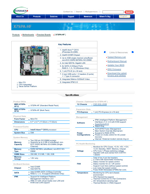
English
Links & Resources Tested Memory List Motherboard Manual Update Your BIOS IPMI Firmware Download the Latest Drivers and Utilities
ACPI/APM Power Management Main Switch Override Mechanism Suspend to RAM (STR) Poweron mode control for AC power recovery Internal / External modem remote ringon
OS Compatibility
• Please see our OS Compatibility Chart
LED
Other Features
CPU / System Overheat LED
Chassis intrusion Detection Chassis intrusion Header SDDC Support
Temperature
Monitoring for CPU and chassis environment CPU thermal trip support Thermal Control for 2 x Fan Connectors I2C temperature sensing logic Thermal Monitor 2 (TM2) Support
2. Intel® ICH9R Chipset 3. Up to 4GB single channel unbuffered,
FPGA可编程逻辑器件芯片XC7K325T-2FFG900CES中文规格书

UltraScale Architecture-Based FPGAs Memory IP v1.4 PG150 January 21, 2021Chapter19Design Flow StepsThis chapter describes customizing and generating the core, constraining the core, and the simulation, synthesis and implementation steps that are specific to this IP core. Moredetailed information about the standard Vivado® design flows and the Vivado IP integrator can be found in the following Vivado Design Suite user guides:•Vivado Design Suite User Guide: Designing IP Subsystems using IP Integrator (UG994) [Ref13]•Vivado Design Suite User Guide: Designing with IP (UG896) [Ref14]•Vivado Design Suite User Guide: Getting Started (UG910) [Ref15]•Vivado Design Suite User Guide: Logic Simulation (UG900) [Ref16]Customizing and Generating the Corecreating projects, defining IP or managed IP projects, and creating block designs.This section includes information about using Xilinx® tools to customize and generate the core in the Vivado Design Suite.If you are customizing and generating the core in the IP integrator, see the Vivado Design Suite User Guide: Designing IP Subsystems using IP Integrator (UG994) [Ref13] for detailed information. IP integrator might auto-compute certain configuration values whenvalidating or generating the design. To check whether the values change, see thedescription of the parameter in this chapter. To view the parameter value, run thevalidate_bd_design command in the Tcl Console.You can customize the IP for use in your design by specifying values for the variousparameters associated with the IP core using the following steps:1.Select the IP from the Vivado IP catalog.2.Double-click the selected IP or select the Customize IP command from the toolbar orright-click menu.UltraScale Architecture-Based FPGAs Memory IP v1.4 PG150 January 21, 2021Chapter 38:Debuggingvio_tg_instr_victim_mode I3Victim mode to be programmed.One victim bit could be programmed using global register vio_tg_victim_bit.The rest of the bits on signal bus are considered to be aggressors.The following program options define aggressor behavior: NO_VICTIM = 0;HELD1 = 1; // All aggressor signals held at 1HELD0 = 2; // All aggressor signals held at 0NONINV_AGGR = 3; // All aggressor signals are same as victimINV_AGGR = 4; // All aggressor signals are inversion of victimDELAYED_AGGR = 5; // All aggressor signals are delayed version of victim (num of cycle of delay is programmed at vio_tg_victim_aggr_delay)DELAYED_VICTIM = 6; // Victim signal is delayed version of all aggressorsCAL_CPLX = 7; Complex Calibration pattern (Must be programed along with Data Mode CAL_CPLX)vio_tg_instr_victim_aggr_delay I5Define aggressor/victim pattern to be N-delay cycle of victim/aggressor.It is used when victim mode "DELAY_AGGR" or "DELAY VICTIM" mode is used in traffic pattern.vio_tg_instr_victim_select I3Victim bit behavior programmed.VICTIM_EXTERNAL = 0; // Use Victim bit provided invio_tg_glb_victim_bitVICTIM_ROTATE4 = 1; // Victim bit rotates from Bit[0] to Bit[3] for every NibbleVICTIM_ROTATE8 = 2; // Victim bit rotates from Bit[0] to Bit[7] for every byteVICTIM_ROTATE_ALL = 3; // Victim bit rotates through all bitsvio_tg_instr_num_of_iter I32Number of Read/Write commands to issue (number of issuemust be > 0 for each instruction programmed)vio_tg_instr_m_nops_btw_n_burst_m I10M: Number of NOP cycles in between Read/Write commands at User interface at general interconnect clock.N: Number of Read/Write commands before NOP cycle insertion at User interface at general interconnect clock.vio_tg_instr_m_nops_btw_n_burst_n I32M: Number of NOP cycles in between Read/Write commands at User interface at general interconnect clock.N: Number of Read/Write commands before NOP cycle insertion at User interface at general interconnect clock.vio_tg_instr_nxt_instr I6Next instruction to run.To end traffic, next instruction should point at EXIT instruction.6’b000000-6’b011111 – valid instruction6’b1????? – EXIT instructionTable 38-45:Instruction Programming (Cont’d)Instruction Programming I/O Width DescriptionUltraScale Architecture-Based FPGAs Memory IP v1.4 PG150 January 21, 2021Chapter 3:Core ArchitectureTable 3-9:Error Signal DescriptionsSTAGE_NAME Stage Code DDR_CAL_ERROR_1DDR_CAL_ERROR_0ErrorDQS Gate10x1Byte RIU NibbleCalibration uses the calculated latency fromthe MPR register as a starting point and thenbacks off and begins sampling. If the sampleoccurs too late in the DQS burst and thereare no taps left to decrement for the latency,then an error has occurred.0x2Byte RIU Nibble Expected pattern was not found onGT_STATUS.0x3Byte RIU NibbleCAS latency is too low. Calibration starts at aCAS latency (CL) – 3. For allowable CASlatencies, see EXTRA_CMD_DELAYConfiguration Settings, page182.0x4Byte RIU Nibble Pattern not found on GT_STATUS, all 0s weresampled. Expecting to sample the preamble.0x5Byte RIU Nibble Pattern not found on GT_STATUS, all 1s weresampled. Expecting to sample the preamble.0x6Byte RIU Nibble Could not find the 0->1 transition with finetaps in at least 1 tck (estimated) of fine taps.0x7Byte RIU Nibble Underflow of coarse taps when trying to limitmaximum coarse tap setting.0x8Byte RIU Nibble Violation of maximum read latency limit.0x9Byte RIU Nibble Data check failed with DQS gate settings andread latency range has been exhausted.DQS Gate SanityCheck20xF N/A N/A PHY fails to return same number of data bursts as expectedWrite Leveling30x1Byte N/A Cannot find stable 0.0x2Byte N/A Cannot find stable 1.0x3Byte N/A Cannot find the left edge of noise region withfine taps.0x4Byte N/ACould not find the 0->1 transition with finetaps in at least 1 tck (estimated) of ODELAYtaps.Read Per-Bit Deskew40x1Nibble Bit No valid data found for a given bit in thenibble when running the deskew pattern.0xF Nibble Bit Timeout error waiting for read data bursts toreturn.。
BLM15HD182SN1磁珠规格书

BD
BX
PD
PG For Power Lines
PN
PX
KG For Power Lines (Low DC Resistance Type)
SG
HG
For GHz Band General Use
EB
For GHz Band High-speed Signal Lines (Low Direct Current Type)
Chip Ferrite Bead for Automotive Part Numbering
(Part Number)
BL M 18 AG 102 S Z 1 D q w e r t y u io
qProduct ID Product ID BL
Chip Ferrite Beads
wType Code E M
Impedance (Ω)
at 100MHz
at 1GHz
10 (Typ.)
-
70 (Typ.)
-
120±25%
-
240±25%
-
10 (Typ.)
-
70 (Typ.)
-
120±25%
-
220±25%
-
600±25%
-
1000±25%
-
600±25%
140 (Typ.)
1000±25%
300 (Typ.)
0402
For High Speed Signal (Sharp impedance characteristics)
For Large Current For Standard
GHz Range
For High Speed Signal
- 1、下载文档前请自行甄别文档内容的完整性,平台不提供额外的编辑、内容补充、找答案等附加服务。
- 2、"仅部分预览"的文档,不可在线预览部分如存在完整性等问题,可反馈申请退款(可完整预览的文档不适用该条件!)。
- 3、如文档侵犯您的权益,请联系客服反馈,我们会尽快为您处理(人工客服工作时间:9:00-18:30)。
LVDS 信号
11
LAX2-
LVDS 信号
12
LAX2+
LVDS 信号
13
GND
14
LACK-
15
LACK+
LVDS 信号
16
GND
LVDS 信号
17
LAX3-
LVDS 信号
18
LAX3+
LVDS 信号
19
GND
GND
20
NG
液晶屏接口 1
请参见 EJ070NA-01J 屏规 格书
6 运输,存储,使用要求 1,不要重压和弯折变形 2,防静电和水 3,相对湿度,小于 80% 4, 使用温度 -1-度--+60 度 5,使用湿度 0-+40 度
特殊
支持 LED 背光驱动
4 产品外观尺寸 5 产品结构说明 驱动板尺寸:54.2MMX27.5MM
6:驱动板实物图:
7,AD 板接口功能说明 序号
1 2 3 8 接口功能详细说明 8.1
接口 6PIN CON3 CON1
说明 LED 背光控制输入 LVDS 信号输入 液晶屏接口
6PIN 接口(此接口,默认不按装需要调整,请参见以下技术调整说明)
如有其它相关的此驱动板相关的技术类问题,请致电我公司,
2 特性说明 输入信号 接口
电源
LBIT(默认)
标准 LVDS 信号接 DF14-20P 口
屏接口 INVERTER 接口
40PIN-0.5MM 标准 EJ080NA-04C 定义 6PIN 标准插座(默认不安装)
输入电源
同屏供电 3.3V(不需要另外设置)
背光供电类型
R33
R36
6PIN
备注
3.3V
10R 磁珠
10K 电阻
NC
当半默认状态
5V
NC
NC
装 6PIN-2.0 排座 需要技术改进,但
一定要注意拆除
两个位号上的元
件在通电,否则有
可能会损坏液晶
屏和相关电路板
的可能,损失重大
3,背光供电不得大于 6V,,否则有可能会损坏背光驱动 IC,或液晶屏 4,背光的开关信号,不得大于 5V,否则有可能会损坏背光驱动 IC,
2,本驱动板可以支持,EJ070NA-01J, EJ080NA-04B EJ080NA-04C EJ101NA-01
等,通用的 40PIN 液晶屏,或是功能相同的定义的液晶屏(也可以咨询我公司技术部)
3,本驱动板,LVDS 信号输入采用标准的 DF14-20P 接口,且接口定义采用市面上通用的单 8(8bit) 通用 LVDS 信号线,我公司有相关的配套线材,需要另外付费,
在进行驱动板技术功能设置时,请仔细阅读以下说明,并在技术改进时,注意正确操作,以免损坏驱 动板或液晶屏
1,默认 8BIT 的信号输入用不能调整
2,关于背光输入和开关控制部分的设置
本驱动板默认一条 LVDS 信号线输入,并在液晶屏供电的 3.3V,取 LED 背光供电和开关控制信号
当液晶屏需要电流较大,或在使用高亮度液晶屏时,没有达到正常的亮度时,可按以下改进
液晶驱动板规格书 产品名称 TYT-800182 驱动板 文件编号 TYT2013112801
供应商:
地址: 联系人 : 客户名称: 客户地址: 联系人 文件级别 公共文件 发布日期 2013-11-28
1.产品说明: 1,本驱动板是一款 LVDS 信号输入,LVDS 信号直通输出,并集成了 LED 背光驱动,同时可以产 生,AVDD, VGL ,VGH,VCOM,等多路电压的液晶屏转接板
4, 本驱动板默认 8BIT 的标准 LVDS 信号输入, 5,如果现在的背光不能达到亮度要求,可以 参见以下技术说明,自行设置
6,本驱动板,电容元件,采用三星的品牌,工作温度可达-50 度到 120 度 7,本驱动板,电阻元件,采用台湾厚生品牌,工作温度可达-50 度到 120 度 8,本驱动板综合工作温度可在-20 度到 50 度 9,本驱动板,默认为有铅产品,如需要 ROHS 标准或达到军工级标准,请联系我公司, 其它相关的技术问题可咨询我公司技术部
1
+5V
正电源输入
2
+5V
正电源输入
3
EN
高压板开关信号
4
空
空
5
GND
GND
6
GND
GND
J4-----LVDS 屏接口 序号
定义
说明
1
VCC
液晶屏供电
2
VCC
液晶屏供电
3
GND
地
4
GND
地
5
LAX0-
地
6
LAX0+
地
7
GND
LVDS 信号
8
LAX1-
LVDS 信号
9
LAX1+
LVDS 信号
10
GND