ACPL332J应用
CommScope Flex Max RF Amplifiers FM332 1.2 GHz Lin

DATA SHEET Flex Max ®RF Amplifiers FM3321.2 GHz Line Extender AmplifierFor cable operators looking to ensure scalability, maximum backward compatibility, and protect network investments, CommScope offers solutions that deliver new services with minimal CAPEX, enhance network efficiency, and increase subscriber satisfaction.The new CommScope 1.2 GHz Flex Max ®FM332 Line Extender Amplifier enables cable operators to take advantage of DOCSIS 3.1 efficiencies while maintaining backward compatibility with existing 750 MHz, 870 MHz, and 1 GHz systems.•Supports 1.2 GHz Downstream and 204 MHzUpstream bandpass for DOCSIS ®3.1 migration•Increased gain to allow drop in upgrades for≥ 750 MHz spacing•Modular RF Electronics package with upgradablefrequency split options•Mechanically compatible with legacyE7/FM330/FM331 amplifier housings•QAM and Analog ADU options for automaticlevel control and gain hold in the event ofpilot loss FEATURESDownstreamThe FM332 is equipped with Gallium Nitride (GaN) hybrid technology and a single high‐level driven RF output. New 1.2 GHz Forward Cable Equalizers (CE‐120‐*) and Cable Simulators (CS‐120‐*) are available to optimize system designs. These new plug‐ins are in the JXP‐style form factor and plug into a carrier board with a backward compatible footprint, so operators who want to use the new amplifiers in older 870 MHz or 1 GHz systems can re‐use their legacy SEQ‐* equalizers.FM332 line extenders feature a new series of plug‐in Automatic Level Control (ALC) boards that include standard 711 MHz and 609 MHz QAM as well an option for legacy 499.25 MHz analog pilot frequencies. The amplifier utilizes a gain hold feature in the event of pilot loss for added system reliability. If Manual Level Control (MLC) option is chosen, there is an Automatic/Manual mode jumper that can be set to enable the amplifier to operate in Thermal Gain Control mode. There is an LED indicator to provide visual confirmation of the selected mode and pilot presence.The FM332 utilizes pluggable filters, which provides operators with the flexibility to change band splits in the future. The following frequency splits are available:•5 to 42 MHz/54 to 1218 MHz (042 split)•5 to 85 MHz/102 to 1218 MHz (085 split)•5 to 204 MHz/258 to 1218 MHz (204 split)UpstreamThe FM332 features 27 dB of gain in the upstream to accommodate a wide variety of network designs including high split. The upstream circuitry includes a single attenuator location prior to the output test point that allows operators to set levels. The return equalizer maintains the MEQ‐**‐* form factor from the FM331, and operators can select MEQ return path equalizers based on the diplex split and values required in their network design. Previous generation MEQT return path equalizers are no longer required because of the FM332’s on‐board thermal compensation feature, which helps maintain levels over temperature.Backward CompatibilityThe FM332 RF Module is backward compatible with the previous versions of FM330 and FM331 amplifier housings. Earlier E5 and E7 housings require a baseplate kit and performance > 1 GHz is not guaranteed.COMPATIBILITY330331 Upgrade to FM332Yes*Yes*Yes Yes*Requires Baseplate Upgrade Kit part number 1500855‐001 ‐Performance > 1 GHz not guaranteed204 Split258–1218 Flatness, dB2±0.75 Operational Gain, dB338 minInternal Slope, dB4042 Split085 Split204 Split 11.9 11.1 9.0Noise Figure, dB57.5 max @ 54 MHz9.0 @ 1218 MHzTest Point, dB20 ±1.0Return Loss, dB16Hum Modulation @ 15A, dBc6F minfwd to 870 MHz871 to 1003 MHz1004 to 1218 MHz ‐60 ‐55‐50Distortion: 1.2 GHz Analog/Digital, 30 Analog/160 Digital Channels7Reference Frequency, MHz1218/258/54Reference Input Level, dBmV19/10.7/9.9 (virtual)Reference Output Level (21 dB Slope), dBmV57/39.7/36 (virtual)Composite Triple Beat (CTB), dBc‐74Composite Second Order (CSO), dBc‐78Carrier to Composite Noise (CCN), dB56Distortion: 1.2 GHz All Digital, 190 Digital ChannelsReference Frequency, MHz1218/258/54Reference Input Level, dBmV13/4.7/3.9 (actual)Reference Output Level (21 dB Slope), dBmV51/33.7/30 (actual)Carrier to Composite Noise (CCN), dB850MER, dB948NOTES:1.Operating passband of station is determined by the diplex filters, forward correction board, and high pass filter installed in the amplifier.2.Flatness is measured with respect to slope. Slope is calculated using least squares.3.Specified at Ta = 25 ±5°C and measured at 1218 MHz.Includes the gain control back‐off of 5.0 ±0.1 dB and forward equalizer loss of 1.0 dB.4.Specified from 54 MHz to 1218 MHz,5.0 dB Linear Slope plus6.9 dB Cable Slope.5.The noise figure is measured with a 1 dB attenuator installed in the forward equalizer location and is specified at Ta = 25 ±5°C. The noise figure may degrade by up to 1 dB over thefull operating temperature range. The applicable specification value for any test frequency between 54 MHz and 1218 MHz is determined by applying linear interpolation to the listed specification values.6.Hum modulation is measured at 15 Arms AC current passing through the port under test.7.30 analog channels from 55.25 MHz to 253.25 MHz, 124 digital QAM channels from 261 MHz to 999 MHz, and a 192 MHz wide OFDM channel centered at 1122 MHz.N is measured by turning off the QAM channel under test and inserting a CW test signal at the corresponding QAM RF level in its place.9.MER is calculated from the measured CCN.204 Split5–204Flatness, dB2±0.5Operational Gain, dB327Slope, dB0 ±0.75Noise Figure, dB4 6.0Test Points, dB20 ±1.0dBReturn Loss, dB516Response Over Temperature, dB6±0.5 maxHum Modulation @ 15A, dBc7‐50, 5–10 MHz‐55, 11–15 MHz-60, 16–F maxreturn MHzDistortion: All Digital, 6 Digital Channels8Reference Frequency, MHz42/5Reference Input Level, dBmV13/13Reference Output Level, dBmV40/40NPR Dynamic Range, dB936BER Dynamic Range, dB1042Distortion: All Digital, 13Digital Channels8Reference Frequency, MHz85/5Reference Input Level, dBmV9/9Reference Output Level, dBmV36/36NPR Dynamic Range, dB933BER Dynamic Range, dB1039Distortion: All Digital, 33Digital Channels8Reference Frequency, MHz204/5Reference Input Level, dBmV6/6Reference Output Level, dBmV33/33NPR Dynamic Range, dB929BER Dynamic Range, dB1035NOTES:1.Upstream bandwidth is determined by the diplex filters, low pass filter (RPLPF), and upstream equalizer (MEQ * *) installed in the amplifier.2.Flatness is measured with respect to slope; slope is linear and calculated using a least squares.3.The operational gain is specified at F maxret and Ta = 25 ±5°C and includes gain control back‐off of 3.0 ±0.1 dB and a reverse equalizer loss of 1.0 dB.4.Specified at Ta = 25 ±5°C. Measured with an MEQ‐0‐0 installed in the reverse equalizer location and a 1 dB attenuator installed in the reverse output pad location. May degrade by upto 1 dB over the full operating temperature range.5.The return loss from 5–15 MHz may degrade by up to 1 dB over the operating temperature range.6.Specified relative to the response measured at Ta = 25 ±5°C.7.Hum modulation is measured at 15 Arms AC current passing through the port under test.8.The QAM load is 256 QAM, J.83 Annex B, 5.360537 MS/s; 6 MHz/channel.9.The NPR dynamic range is specified for an NPR greater than or equal to 40 dB.10.The BER dynamic range is specified for an uncorrected (Pre‐FEC) BER less than or equal to 1.0 x 10‐6.SPECIFICATIONSAC Input Current (Typical)0.81 A/25 W @ 45 V0.36 A/22.5 W @ 75 V0.30 A/22.5 W @ 90 VAC Input Voltage Range, VAC45–90AC Bypass Current, A15Operating Temperature Range‐40°to +60°C‐40°to +140°FHousing Dimensions, L x W x D12.3 x 9.6 x 3.5 inches312 x 243 x 89 mmWeight9 lbs4 kgNote: Specifications are subject to change without notice.Copyright Statement:©2022CommScope,Inc.All rights reserved.ARRIS,the ARRIS logo,and Flex Max are trademarks of CommScope,Inc.and/or its affiliates.All other trademarks are the property of their respective owners.No part of this content may be reproduced in any form or by any means or used to make any derivative work (such as translation,transformation,or adaptation)without written permission from CommScope,Inc and/or its affiliates (“CommScope”).CommScope reserves the right to revise or change this content from time to time without obligation on the part of CommScope to provide notification of such revision or change.Contact Technical Services for product support:•United States: +1‐888‐944‐4357•International: +1‐215‐323‐2345RELATED PRODUCTSADU/QADUOptical Nodes FM902 1.2 GHz Trunk/BridgerFrequency Split Upgrade Kits Forward Signal CorrectionPlug ‐in Accessories Installation Services1.2 GHz FM332 LINE EXTENDER ORDERING GUIDEIn the example below, part number FML12X085‐SHMPR1N corresponds to the shaded rows in the Key Guide.F M L 12X 085—S H M P R 1N REQUIRED ACCESSORIESModel NameDescription CE ‐120‐*CS ‐120‐*Forward1.2GHzCable Equalizer 2 to 20 dB in 1 dB steps ‐or ‐Forward 1.2 GHz Cable Simulator 1 to 10 dB in 1 dB steps MEQ ‐**‐*Return Equalizer, 5–42 MHz (042 Split), 5–85 MHz (085 Split), 5–204 MHz (204 Split)NPB ‐*NPB ‐750Plug ‐in attenuator/pad (values 0 to 26 dB in 1 dB steps)Plug ‐in terminator (75 ohm)。
乐泰332中文技术参数

机械性能
使用活化剂 7387
剪切强度 ASTM D 1002, 标准钢试样, psi
无间隙
3000
0.010”间隙
1400
0.020”间隙
1500
180° 耐剥离, piw
20
耐环境性能
所 有 数 据 均 通 过 对 标 准 钢 制 搭 剪 试 样 (ASTM D1002)测得的。在进行环境暴露试验前,胶粘剂 在室温下固化 48 小时。粘结件无间隙。
Brookfield RVF 粘度测量计
7#转子, @20rpm, cP
75,000-130,000
固化性能 活化剂固化 本产品使用活化剂 7387,可以室温固化。通过确 定固定时间(操作时间)和固化速度的关系,即粘接 强度随时间的变化,来衡量固化特性。试验中使 用 ASTM D1002 中规定的钢制搭剪试样。试验中 样品不进行喷砂以及清洗处理。试验操作在室温 下进行。这里提供的信息仅可供参考使用,因为 实验数据取决于被测试样的本质。具体应用中, 数据应当通过对实际被粘结部件在生产条件下进 行试验获得。
3. 在另一被胶粘表面上涂胶粘剂。
4. 配合胶粘表面,施加压力使胶粘剂薄薄地均匀 分布。在使用活化剂 2 小时内要接合胶粘表面 (活化剂在部件上的活性时间为两小时)。减小 活化剂在部件上的时间可以增加粘结性能。
5. 压紧直到被粘结件具有一定的可操作强度。可 操作强度随部件的几何形状,表面积和配合公 差的不同而异。
本产品为单组分,在乐泰活化剂 7387 的帮助下, 可以在室温固化。
典型用途 在电动机磁铁粘接应用中用于永磁铁的固定。
固化前材料典型性能
粘合剂
典型值
基础树脂
改性的丙烯酸类
ACPL-331J CN的中文资料

ACPL-331J 1.5A电流输出的IGBT门极驱动光耦集成的(Vce)饱和度检测,欠压锁定,故障状态反馈和有源米勒钳位综述:ACPL - 331J是一种先进的1.5 A的输出电流,方便易用的智能化的门极驱动器使得IGBT的Vce的故障保护更加紧凑,价格合理,且易于实现功能,如集成的Vce检测,欠压锁定(UVLO),IGBT的“软”关断,隔离的集电极开路故障反馈和有源米勒钳位提供最大的设计灵活性和保护电路。
ACPL - 331J包含了一个GaAsP的LED。
通过该LED完成光电信号的耦合。
ACPL-331J非常适合用于驱动电机控制领域的功率IGBT和MOSFET。
这些光耦的电压、电流供给使其非常适用用于直接驱动1200V 100A以下的IGBT。
对于更高功率等级的IGBT,ACPL-331J通常被用来驱动由分离器件构成的IGBT门极驱动器。
ACPL-331J具备一个峰值为891V的绝缘电压。
结构框图:产品特点:z滞后的欠压封锁功能z饱和度侦测z米勒钳位z隔离的开路集电极故障反馈z IGBT软关断z IGBT下个开通周期的故障复位z提供SO - 16封装z安规认证详细说明:z 1.5A的最大输出峰值电流z 1.0A的最小输出峰值电流z温度范围内最大250nS的传输延时z100nS最大脉冲宽度失真z在V CM = 1500 V时,最小15 kV/µs的共模抑制能力z最大供电电流I CC(max) < 5 mAz温度范围内工作电压可达15V-30Vz1A的米勒钳位。
该脚不用时必须同VEE短接z宽的工作温度范围:–40°C to 100°C应用:z IGBT和功率MOSFET的驱动z交流和直流无刷电机驱动z变频器和UPS引脚功能介绍订货信息ACPL-331J 经过3750 Vrms 1分钟测试,符合UL1577标准。
备注 表面 符合IEC / EN产品编号 符合ROHS 标准 封装方式 安装 卷带装 DIN EN 60747-5-2 数量-000E SO-16 X X 45/管ACPL-331J -500E X X X 850/卷 订购时,从产品编号列表中选择产品编号,并结合其他所需的选项形成定单输入。
AP332产品手册

优势:为高密度场景提供企业级的无线网络减轻IT 部门负担,降低拥有成本提供灵活的部署选项支持最先的标准,同时老终端为支持您企业的应用提供扩展性AP332双射频模块,双频,3x3:3空间流802.11n AP功能与灵活性符合您的无线网络需求, 性能超乎您的预期AP332是双射频模块,3空间流的802.11n 无线接入点,专门用于数据、语音、视频应用的企业级网络。
AP332的每组射频卡提供450Mbps 空口接入速率,整机可以接入256个客户端。
AP332使得您的敏感应用,特别是在高密度要求下的环境表现依然值得信赖。
AP332能够同时支持多个资源密集型应用,最大限度的提高您企业生产力。
即插用的部署方式可以降低IT 部门的负担。
AP332还使得您可以非常便捷的部署一套可信赖的802.11n 网络,而且AP332对传统 802.11a/b/g 终端设备具有良好的兼容性。
更多关于AP332的产品信息,请访问 或者AP332可以提供无比拟的Meru 虚拟无线网络架构。
AP332为您选择内置或者外置天线提供灵活性。
和其他Meru 无线接入点一样,她可以无缝兼容所有Meru 控制器、System DirecSystem 管理系统、Meru 其他管理工具,从而为您的无线网络 提供智能化管理和流量控制的可能 管理和流量控制的可能。
功能特性:同时支持数据、语音和视频的应用零配置,即插用内置和外天线同时支持2.4GHz 5GHz 的 802.11n ,支持传统a/b/ga/b/g 终端设备兼容所有Meru 控制器和System Director 管理系统物理参数尺寸AP332i或者AP332e(包括支架)7. 09 ”(18.0cm) 长,7.09”(18.0cm) 宽,2.67”(6.77cm) 高重量AP332i(包括支架)2lbs 5.3 oz. (1057g)SafetyUL 60950-1; IEC 60950-1; CAN/CSA-C22.2No. 60950-1IEC 60950-1。
FCN1206A332J-H3中文资料
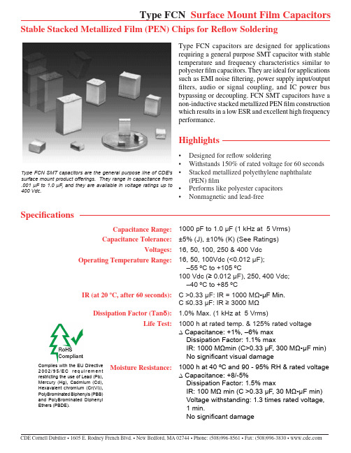
SpecificationsType FCN capacitors are designed for applicationsrequiring a general purpose SMT capacitor with stabletemperature and frequency characteristics similar topolyester film capacitors. They are ideal for applicationssuch as EMI noise filtering, power supply input/outputfilters, audio or signal coupling, and IC power busbypassing or decoupling. FCN SMT capacitors have anon-inductive stacked metallized PEN film constructionwhich results in a low ESR and excellent high frequencyperformance.HighlightsDesigned for reflow solderingWithstands 150% of rated voltage for 60 secondsStacked metallized polyethylene naphthalate(PEN) filmPerforms like polyester capacitorsNonmagnetic and lead-free•••••Capacitance Range:Capacitance Tolerance:Voltages:Operating Temperature Range:IR (at 20 ºC, after 60 seconds):Dissipation Factor (Tanδ):Life Test:Moisture Resistance:1000 pF to 1.0 µF (1 kHz at 5 Vrms)±5% (J), ±10% (K) (See Ratings)16, 50, 100, 250 & 400 Vdc16, 50, 100Vdc (<0.012 µF);–55 ºC to +105 ºC100 Vdc (≥ 0.012 µF), 250, 400 Vdc;–40 ºC to +85 ºCC >0.33 µF: IR = 1000 MΩ•µF Min.C ≤0.33 µF: IR ≥ 3000 MΩ1.0% Max. (1 kHz at 5 Vrms)1000 h at rated temp. & 125% rated voltage∆ Capacitance: +1%, –6% maxDissipation Factor: 1.1% maxIR: 1000 MΩmin (C>0.33 µF, 300 MΩ•µF min)No significant visual damage1000 h at 40 ºC and 90 - 95% RH & rated voltage∆ Capacitance: +8/-5%Dissipation Factor: 1.5% maxIR: 100 MΩ min (C >0.33 µF, 30 MΩ•µF min)Voltage withstanding: 1.3 times rated voltage,1 min.No significant damageStable Stacked Metallized Film (PEN) Chips for Reflow SolderingT ype FCN SMT capacitors are the general purpose line of CDE’ssurface mount product offerings. They range in capacitance from.001 µF to 1.0 µF, and they are available in voltage ratings up to400 Vdc.Complies with the EU Directive2002/95/E C r e q u i r e m e n trestricting the use of Lead (Pb),Mercury (Hg), Cadmium (Cd),Hexavalent chromium (Cr(VI)),PolyBrominated Biphenyls (PBB)and PolyBrominated DiphenylEthers (PBDE).Part Numbering SystemSpecificationsResistance to Soldering Heat:5 s at max capacitor surface temperature ∆ Capacitance: ±5% maxDissipation Factor: 1.1% maxIR: 1000 MΩ min (C >0.33 µF, 300 MΩ•µF min)Voltage withstanding: 1.5 times rated voltage, 1 min.No significant visual damage.Surface Temperature:16 V & 50 V & 100 V ≤ 0.01 µF: 240 ºC max 100 V ≥ 0.012 µF, 250 V & 400 V: 230 ºC maxMoisture Resistance:500 h at 85 ºC and 85% RH ∆ Capacitance: ±10% max Dissipation Factor: 2% maxIR: 10 MΩ min (C >0.33 µF, 3 MΩ•µF min) Voltage withstanding: 1.3 times rated voltage, 1 min.No significant damageWithstand Voltage:16 V & 50 V, 100 V ≤ 0.01 µF: 175% rated voltage, 5 s100 V ≥ 0.012 µF, 250 V and 400 V: 150% rated voltage, 5 sFCN1206A102JH2TapeTape PackagingWidth Diameter Reel Type Case SizeVoltage Capacitance Tolerance Code (mm)[in.(mm)]QuantityFCN1206C = 16 Vdc 102 = 0.001 µF J = ±5%K1=87 (178)40001913H = 50 Vdc 223 = 0.022 µF K = ±10%J1, J2=87 (178)30002416 A = 100 Vdc 474 = 0.47 µFH1, H2=87 (178)30002420E = 250 Vdc H3=87 (178)20002820G = 400 VdcG1, G2, G3=87 (178)20003022E1, E2=1213 (330)30003925E3, E4=1213 (330)20003931D1, D2=1213 (330)30006031D3, D4, D5=1213 (330)20006040B, Z =1213 (330)1500U, V, X, Y =1613 (330)1000S, T=2413 (330)750Outline Drawingt L WTt = 0.014 ± 0.008 in. (0.35 ±0.2 mm)For 0.001 µF – 0.01 µF, 100 V, t = 0.026 ±0.012 in. (0.62 ± 0.3 mm) RatingsCap Catalog L W T(µF)Part Number in (mm)in (mm)in (mm)16 Vdc.12FCN1913C124J-E10.189±0.008 (4.8±0.2)0.130±0.012 (3.3±0.3)0.055±0.008 (1.4±0.2) .15FCN1913C154J-E20.189±0.008 (4.8±0.2)0.130±0.012 (3.3±0.3)0.079±0.008 (2.0±0.2) .18FCN1913C184J-E20.189±0.008 (4.8±0.2)0.130±0.012 (3.3±0.3)0.079±0.008 (2.0±0.2) .22FCN1913C224J-E40.189±0.008 (4.8±0.2)0.130±0.012 (3.3±0.3)0.094±0.008 (2.4±0.2) .27FCN2416C274J-D10.236±0.008 (6.0±0.2)0.161±0.012 (4.1±0.3)0.071±0.008 (1.8±0.2) .33FCN2416C334J-D20.236±0.008 (6.0±0.2)0.161±0.012 (4.1±0.3)0.079±0.008 (2.0±0.2) .39FCN2416C394J-D30.236±0.008 (6.0±0.2)0.161±0.012 (4.1±0.3)0.094±0.008 (2.4±0.2) .47FCN2416C474J-D40.236±0.008 (6.0±0.2)0.161±0.012 (4.1±0.3)0.110±0.008 (2.8±0.2)50 Vdc.056FCN1913H563J-E20.189±0.008 (4.8±0.3)0.130±0.012 (3.3±0.3)0.055±0.008 (1.4±0.2) .068FCN1913H683J-E20.189±0.008 (4.8±0.3)0.130±0.012 (3.3±0.3)0.079±0.008 (2.0±0.2) .082FCN1913H823J-E40.189±0.008 (4.8±0.3)0.130±0.012 (3.3±0.3)0.079±0.008 (2.0±0.2) .10FCN1913H104J-E30.189±0.008 (4.8±0.3)0.130±0.012 (3.3±0.3)0.094±0.008 (2.4±0.2) .12FCN2416H124J-D10.236±0.008 (6.0±0.2)0.161±0.012 (4.1±0.3)0.071±0.008 (1.8±0.2) .15FCN2416H154J-D20.236±0.008 (6.0±0.2)0.161±0.012 (4.1±0.3)0.079±0.008 (2.0±0.2) .18FCN2416H184J-D30.236±0.008 (6.0±0.2)0.161±0.012 (4.1±0.3)0.094±0.008 (2.4±0.2) .22FCN2416H224J-D40.236±0.008 (6.0±0.2)0.161±0.012 (4.1±0.3)0.110±0.008 (2.8±0.2)100 Vdc.0010FCN1206A102J-H20.126±0.008 (3.2±0.2)0.063±0.012 (1.6±0.3)0.043±0.008 (1.1±0.2) .0012FCN1206A122J-H20.126±0.008 (3.2±0.2)0.063±0.012 (1.6±0.3)0.043±0.008 (1.1±0.2) .0015FCN1206A152J-H20.126±0.008 (3.2±0.2)0.063±0.012 (1.6±0.3)0.043±0.008 (1.1±0.2) .0018FCN1206A182J-H20.126±0.008 (3.2±0.2)0.063±0.012 (1.6±0.3)0.043±0.008 (1.1±0.2) .0022FCN1206A222J-H20.126±0.008 (3.2±0.2)0.063±0.012 (1.6±0.3)0.043±0.008 (1.1±0.2) .0027FCN1206A272J-H20.126±0.008 (3.2±0.2)0.063±0.012 (1.6±0.3)0.043±0.008 (1.1±0.2) .0033FCN1206A332J-H30.126±0.008 (3.2±0.2)0.063±0.012 (1.6±0.3)0.059±0.008 (1.5±0.2) .0039FCN1206A392J-H30.126±0.008 (3.2±0.2)0.063±0.012 (1.6±0.3)0.059±0.008 (1.5±0.2) .0047FCN1206A472J-H30.126±0.008 (3.2±0.2)0.063±0.012 (1.6±0.3)0.059±0.008 (1.5±0.2) .0056FCN1210A562J-G20.126±0.008 (3.2±0.2)0.063±0.012 (1.6±0.3)0.059±0.008 (1.5±0.2) .0068FCN1210A682J-G20.126±0.008 (3.2±0.2)0.063±0.012 (1.6±0.3)0.059±0.008 (1.5±0.2) .0082FCN1210A822J-G30.126±0.008 (3.2±0.2)0.063±0.012 (1.6±0.3)0.083±0.008 (2.1±0.2) .010FCN1210A103J-G30.126±0.008 (3.2±0.2)0.063±0.012 (1.6±0.3)0.083±0.008 (2.1±0.2) .012FCN1913A123K-E10.189±0.008 (4.8±0.2)0.189±0.008 (3.3±0.3)0.055±0.008 (1.4±0.2) .015FCN1913A153K-E10.189±0.008 (4.8±0.2)0.189±0.008 (3.3±0.3)0.055±0.008 (1.4±0.2) .018FCN1913A183K-E10.189±0.008 (4.8±0.2)0.189±0.008 (3.3±0.3)0.055±0.008 (1.4±0.2) .022FCN1913A223K-E10.189±0.008 (4.8±0.2)0.189±0.008 (3.3±0.3)0.055±0.008 (1.4±0.2) .027FCN1913A273K-E10.189±0.008 (4.8±0.2)0.189±0.008 (3.3±0.3)0.055±0.008 (1.4±0.2) .033FCN1913A333K-E10.189±0.008 (4.8±0.2)0.189±0.008 (3.3±0.3)0.055±0.008 (1.4±0.2) .039FCN1913A393K-E10.189±0.008 (4.8±0.2)0.189±0.008 (3.3±0.3)0.055±0.008 (1.4±0.2)Cap Catalog L W T(µF)Part Number in (mm)in (mm)in (mm)100 Vdc.047FCN1913A473K-E20.189±0.008 (4.8±0.2)0.189±0.008 (3.3±0.3)0.079±0.008 (2.0±0.2) .056FCN1913A563K-E20.189±0.008 (4.8±0.2)0.189±0.008 (3.3±0.3)0.079±0.008 (2.0±0.2) .068FCN1913A683K-E40.189±0.008 (4.8±0.2)0.189±0.008 (3.3±0.3)0.094±0.008 (2.4±0.2) .082FCN1913A823K-E30.189±0.008 (4.8±0.2)0.189±0.008 (3.3±0.3)0.110±0.012 (2.8±0.3) .10FCN2416A104K-D10.189±0.008 (4.8±0.2)0.236±0.008 (6.0±0.2)0.071±0.012 (1.8±0.3) .12FCN2416A124K-D3*0.189±0.008 (4.8±0.2)0.236±0.008 (6.0±0.2)0.099±0.012 (2.4±0.3) .15FCN2416A154K-D4*0.189±0.008 (4.8±0.2)0.236±0.008 (6.0±0.2)0.110±0.012 (2.8±0.3) .18FCN2820A184K-Z0.280±0.016 (7.1±0.4)0.197±0.016 (5.0±0.4)0.079±0.012 (2.0±0.3) .22FCN2820A224K-Z0.280±0.016 (7.1±0.4)0.197±0.016 (5.0±0.4)0.094±0.012 (2.4±0.3) .27FCN2820A274K-Z0.280±0.016 (7.1±0.4)0.197±0.016 (5.0±0.4)0.114±0.012 (2.9±0.3) .33FCN2820A334K-Z0.280±0.016 (7.1±0.4)0.197±0.016 (5.0±0.4)0.138±0.012 (3.5±0.3) .39FCN3022A394K-X0.303±0.016 (7.7±0.4)0.217±0.016 (5.5±0.4)0.134±0.012 (3.4±0.3) .47FCN3022A474K-X0.303±0.016 (7.7±0.4)0.217±0.016 (5.5±0.4)0.157±0.012 (4.0±0.3) .56FCN3925A564K-V0.386±0.016 (9.8±0.4)0.248±0.016 (6.3±0.4)0.118±0.012 (3.0±0.3) .68FCN3925A684K-V0.386±0.016 (9.8±0.4)0.248±0.016 (6.3±0.4)0.142±0.012 (3.6±0.3) .82FCN3925A824K-V0.386±0.016 (9.8±0.4)0.248±0.016 (6.3±0.4)0.169±0.012 (4.3±0.3) 1.0FCN3925A105K-V0.386±0.016 (9.8±0.4)0.248±0.016 (6.3±0.4)0.201±0.012 (5.1±0.3)250 Vdc.0010FCN1913E102K-E1*0.189±0.008 (4.8±0.2)0.130±0.012 (3.3±0.3)0.055±0.008 (1.4±0.2) .0012FCN1913E122K-E1*0.189±0.008 (4.8±0.2)0.130±0.012 (3.3±0.3)0.055±0.008 (1.4±0.2) .0015FCN1913E152K-E1*0.189±0.008 (4.8±0.2)0.130±0.012 (3.3±0.3)0.055±0.008 (1.4±0.2) .0018FCN1913E182K-E1*0.189±0.008 (4.8±0.2)0.130±0.012 (3.3±0.3)0.055±0.008 (1.4±0.2) .0022FCN1913E222K-E1*0.189±0.008 (4.8±0.2)0.130±0.012 (3.3±0.3)0.055±0.008 (1.4±0.2) .0027FCN1913E272K-E1*0.189±0.008 (4.8±0.2)0.130±0.012 (3.3±0.3)0.055±0.008 (1.4±0.2) .0033FCN1913E332K-E1*0.189±0.008 (4.8±0.2)0.130±0.012 (3.3±0.3)0.055±0.008 (1.4±0.2) .0039FCN1913E392K-E1*0.189±0.008 (4.8±0.2)0.130±0.012 (3.3±0.3)0.055±0.008 (1.4±0.2) .0047FCN1913E472K-E1*0.189±0.008 (4.8±0.2)0.130±0.012 (3.3±0.3)0.055±0.008 (1.4±0.2) .0056FCN1913E562K-E1*0.189±0.008 (4.8±0.2)0.130±0.012 (3.3±0.3)0.055±0.008 (1.4±0.2) .0068FCN1913E682K-E1*0.189±0.008 (4.8±0.2)0.130±0.012 (3.3±0.3)0.055±0.008 (1.4±0.2) .0082FCN1913E822K-E1*0.189±0.008 (4.8±0.2)0.130±0.012 (3.3±0.3)0.055±0.008 (1.4±0.2) .010FCN1913E103K-E1*0.189±0.008 (4.8±0.2)0.130±0.012 (3.3±0.3)0.055±0.008 (1.4±0.2) .012FCN1913E123K-E1*0.189±0.008 (4.8±0.2)0.130±0.012 (3.3±0.3)0.055±0.008 (1.4±0.2) .015FCN1913E153K-E1*0.189±0.008 (4.8±0.2)0.130±0.012 (3.3±0.3)0.055±0.008 (1.4±0.2) .018FCN1913E183K-E2*0.189±0.008 (4.8±0.2)0.130±0.012 (3.3±0.3)0.079±0.008 (2.0±0.2) .022FCN1913E223K-E2*0.189±0.008 (4.8±0.2)0.130±0.012 (3.3±0.3)0.094±0.008 (2.4±0.2) .027FCN1913E273K-E4*0.189±0.008 (4.8±0.2)0.130±0.012 (3.3±0.3)0.110±0.008 (2.8±0.2) .033FCN1913E333K-E3*0.189±0.008 (4.8±0.2)0.130±0.012 (3.3±0.3)0.126±0.008 (3.2±0.2) .039FCN2416E393K-D2*0.236±0.008 (6.0±0.2)0.161±0.012 (4.1±0.3)0.079±0.008 (2.0±0.2) .047FCN2416E473K-D3*0.236±0.008 (6.0±0.2)0.161±0.012 (4.1±0.3)0.079±0.008 (2.0±0.2) .056FCN2416E563K-D4*0.236±0.008 (6.0±0.2)0.161±0.012 (4.1±0.3)0.094±0.008 (2.4±0.2) .068FCN2416E683K-D5*0.236±0.008 (6.0±0.2)0.161±0.012 (4.1±0.3)0.110±0.008 (2.8±0.2) .082FCN2420E823K-B*0.236±0.008 (6.0±0.2)0.197±0.016 (5.0±0.4)0.126±0.012 (3.2±0.3) .10FCN2420E104K-B*0.236±0.008 (6.0±0.2)0.197±0.016 (5.0±0.4)0.150±0.012 (3.8±0.3) .12FCN2420E124K-B*0.236±0.008 (6.0±0.2)0.197±0.016 (5.0±0.4)0.177±0.012 (4.5±0.3) .15FCN2825E154K-Y 0.280±0.016 (7.1±0.4)0.248±0.016 (6.3±0.4)0.138±0.012 (3.5±0.3) .18FCN2825E184K-Y 0.280±0.016 (7.1±0.4)0.248±0.016 (6.3±0.4)0.161±0.012 (4.1±0.3) .22FCN2825E224K-Y 0.280±0.016 (7.1±0.4)0.248±0.016 (6.3±0.4)0.201±0.012 (5.1±0.3) .27FCN3925E274K-V 0.386±0.020 (9.8±0.5)0.248±0.016 (6.3±0.4)0.154±0.012 (3.9±0.3)Cap Catalog L W T(µF)Part Number in (mm)in (mm)in (mm)250 Vdc.33FCN3925E334K-V 0.386±0.020 (9.8±0.5)0.248±0.016 (6.3±0.4)0.189±0.012 (4.8±0.3) .39FCN3931E394K-U 0.386±0.020 (9.8±0.5)0.315±0.016 (8.0±0.4)0.173±0.012 (4.4±0.3) .47FCN3931E474K-U 0.386±0.020 (9.8±0.5)0.315±0.016 (8.0±0.4)0.209±0.012 (5.3±0.3) .56FCN6031E564K-T 0.598±0.020 (15.2±0.5)0.315±0.016 (8.0±0.4)0.146±0.012 (3.7±0.3) .68FCN6031E684K-T 0.598±0.020 (15.2±0.5)0.315±0.016 (8.0±0.4)0.173±0.012 (4.4±0.3) .82FCN6040E824K-S 0.598±0.020 (15.2±0.5)0.394±0.016 (10.0±0.4)0.165±0.012 (4.2±0.3) 1.0FCN6040E105K-S 0.598±0.020 (15.2±0.5)0.394±0.016 (10.0±0.4)0.201±0.012 (5.1±0.3)400 Vdc.0010FCN1913G102J-E10.189±0.008 (4.8±0.2) 0.130±0.012 (3.3±0.3) 0.055±0.008 (1.4±0.2) .0012FCN1913G122J-E1 0.189±0.008 (4.8±0.2) 0.130±0.012 (3.3±0.3) 0.055±0.008 (1.4±0.2) .0015FCN1913G152J-E1 0.189±0.008 (4.8±0.2) 0.130±0.012 (3.3±0.3) 0.055±0.008 (1.4±0.2) .0018FCN1913G182J-E1 0.189±0.008 (4.8±0.2) 0.130±0.012 (3.3±0.3) 0.055±0.008 (1.4±0.2) .0022FCN1913G222J-E1 0.189±0.008 (4.8±0.2) 0.130±0.012 (3.3±0.3) 0.055±0.008 (1.4±0.2) .0027FCN1913G272J-E1 0.189±0.008 (4.8±0.2) 0.130±0.012 (3.3±0.3) 0.055±0.008 (1.4±0.2) .0033FCN1913G332J-E1 0.189±0.008 (4.8±0.2) 0.130±0.012 (3.3±0.3) 0.055±0.008 (1.4±0.2) .0039FCN1913G392J-E1 0.189±0.008 (4.8±0.2) 0.130±0.012 (3.3±0.3) 0.055±0.008 (1.4±0.2) .0047FCN1913G472J-E1 0.189±0.008 (4.8±0.2) 0.130±0.012 (3.3±0.3) 0.055±0.008 (1.4±0.2) .0056FCN1913G562J-E2 0.189±0.008 (4.8±0.2) 0.130±0.012 (3.3±0.3) 0.079±0.008 (2.0±0.2) .0068FCN1913G682J-E2 0.189±0.008 (4.8±0.2) 0.130±0.012 (3.3±0.3) 0.079±0.008 (2.0±0.2) .0082FCN1913G822J-E4 0.189±0.008 (4.8±0.2) 0.130±0.012 (3.3±0.3) 0.094±0.008 (2.4±0.2) .010FCN1913G103J-E3 0.189±0.008 (4.8±0.2) 0.130±0.012 (3.3±0.3) 0.110±0.008 (2.8±0.2) .012FCN2416G123J-D2 0.236±0.008 (6.0±0.2) 0.161±0.012 (4.1±0.3) 0.079±0.008 (2.0±0.2) .015FCN2416G153J-D3 0.236±0.008 (6.0±0.2) 0.161±0.012 (4.1±0.3) 0.079±0.008 (2.0±0.2) .018FCN2416G183J-D4 0.236±0.008 (6.0±0.2) 0.161±0.012 (4.1±0.3) 0.110±0.008 (2.8±0.2) .022FCN2416G223J-D5 0.236±0.008 (6.0±0.2) 0.161±0.012 (4.1±0.3) 0.126±0.012 (3.2±0.3) .027FCN2420G273J-B 0.236±0.008 (6.0±0.2) 0.197±0.016 (5.0±0.4) 0.118±0.012 (3.0±0.3) .033FCN2420G333J-B 0.236±0.008 (6.0±0.2) 0.197±0.016 (5.0±0.4) 0.142±0.012 (3.6±0.3) .039FCN2820G393J-Z 0.280±0.016 (7.1±.0.4) 0.197±0.016 (5.0±0.4) 0.126±0.012 (3.2±0.3) .047FCN2820G473J-Z 0.280±0.016 (7.1±.0.4) 0.197±0.016 (5.0±0.4) 0.150±0.012 (3.8±0.3) .056FCN2825G563J-Y 0.280±0.016 (7.1±.0.4) 0.248±0.016 (6.3±0.4) 0.142±0.012 (3.6±0.3) .068FCN2825G683J-Y0.280±0.016 (7.1±.0.4) 0.248±0.016 (6.3±0.4) 0.173±0.012 (4.4±0.3) .082FCN3925G823J-V 0.386±0.016 (9.8±0.4)0.248±0.016 (6.3±0.4) 0.134±0.012 (3.4±0.3) .10FCN3925G104J-V 0.386±0.016 (9.8±0.4)0.248±0.016 (6.3±0.4) 0.157±0.012 (4.0±0.3) .12FCN3931G124J-U 0.386±0.016 (9.8±0.4)0.315±0.016 (8.0±0.4) 0.150±0.012 (3.8±0.3) .15FCN3931G154J-U 0.386±0.016 (9.8±0.4)0.315±0.016 (8.0±0.4) 0.181±0.012 (4.6±0.3)Typical Temperature Characteristics Typical Frequency CharacteristicsVrms vs. Frequency CharacteristicsPulse Handling CapabilityTypical ApplicationsDC Blocking for xDSLIntegration for Electroluminescent (EL) DriverWith no piezoelectric effects to deal with, the SMT film capacitor will not create electrical noise in signal circuits or bu zz ing in power circuits.CapacitanceVoltage dV/dt Capacitance VoltagedV/dt CapacitanceVoltage dV/dt (µF)(Vdc)(volts/µsec)(µF)(Vdc)(volts/µsec)(µF)(Vdc)(volts/µsec).12 - .221660.0039100530.001 - .0039250615.27 - .471640.0047100480.0047 - .033250360.056 - .1050190.0056100450.039 - .12250240.12 - .2250130.0068100410.15 - .22250190.0011001000.0082100370.27 - .47250115.0012100920.01100340.56 - 1.025065.0015100830.012 - .082100320.001 - .0039400615.0018100760.10 - .15100210.0047 - .01400360.0022100690.18 - .33100120.012 - .033400240.0027100630.39 - .47100100.039 - .068400190.0033100570.056 - 1.010070.082 - .15400115。
PL3323中文_Adapter_7W_20130806

V1.0 © 2013
6
Datasheet
PL3323
图 2 辅 绕组电压波形
基于内部的时序 制,辅 绕组的电压可以通过 连接于辅 绕组和 FB 之间的分压电阻采样得
到 在恒压工作模式中,内部误差放大器 采样 的电压进行调节,从而得到恒定的输 电压 在恒流工作模式中,不管系统的输 电压大小, 芯片会保持输 电流恒定
9.7 保护 能
PL3323 内置了多种保护 能,包括 逐周期限 流保护,VDD 钳 保护,软启 , 压保护,短
路保护,开路保护,过压保护,过载保护等 当 PL3323 的 VDD 电压 降到 UVLO(ON),或 者 VDD 电压 升到 OVP 阈值,芯片将不工作,
时会进入重启状态
V1.0 © 2013
0.050 8º
11 注意 项
聚元有权在任何时刻修改 产品信息,恕不另行通知 客户在 单前应确保产品信息的及时更新和完 整性
V1.0 © 2013
8
压保护 过载保护
V1.0 © 2013
2
Datasheet 3 管脚分布图
SOP-8的管脚图如 图所示
PL3323
4 管脚 述
管脚 VDD COMP FB CS DRAIN GND
述 芯片电源输入 误差放大器输 ,用于 路补偿 通过电阻分压连接到辅 绕组,该管脚用于检测输 信号并调节芯片的恒流/恒压 通过检测连接CS到地电阻的电压来反映原边电感电流 高压MOSFET的漏端,连接到变压器 芯片地
℃
7 结构框图
V1.0 © 2013
4
Datasheet
PL3323
8 电气特性
(无特殊说明, 测试条件 参数
ACPL-336J光耦隔离驱动应用笔记

ACPL-336J光耦隔离驱动应⽤笔记说ACPL-336J是光耦隔离驱动的祖先,其实是彻底错误的,因为在它之前AVAGO还有很多个版本。
但是如果说它的⽣⽗AVAGO公司是光耦隔离驱动的祖先应该是没错的。
中功率⼩功率的IGBT保护与驱动,⽤ACPL-336J再好不过了,如果不是特别特别抠成本的话。
AVAGO的IGBT驱动芯⽚我司有上⼗年的应⽤经验,⼩⼩⼀枚芯⽚,表⾯看起来就是搭建外围电路,驱动和保护IGBT,似乎很简单,确实,既然是专⽤驱动芯⽚,只是应⽤,核⼼的关键的东西,都由IC设计⼈员做了,集成到芯⽚⾥⾯了,外围电路的搭建相⽐芯⽚本⾝来说已经简单很多了。
不过⽤这款芯⽚完成基本功能,和⽤它来设计⼀个稳定可靠的产品之间还差⼗万⼋千⾥呢。
所以我感觉,电⼒电⼦领域的单板设计,也是很有搞头的。
有⼈的功率板驱动电路⽼是容易炸管⼦,或者批量应⽤后,⽼是有少量的同种问题出现,却不好定位。
关于这个⽚⼦在应⽤中会遇到哪些具体的问题以及实际的外围电路是什么样⼦的,⽤了哪些器件,参数如何计算,如何实验反馈确定最终参数的,这些问题就不具体说了,毕竟这是⼀家公司需要稍微保留⼀下的技术和经验秘密。
为了增强这部分应⽤思路,现在根据数据⼿册的内容做⼀些记录。
还是先把ACPL_336J的数据⼿册翻译⼀遍吧?DescriptionAvago’s ACPL-336J gate drive optocoupler features fast propagation delay with excellent timing skew performance. Smart features that are integrated to protect the IGBT include IGBT desaturation detection with soft-shutdown protection and fault feedback, undervoltage lockout and feedback, and active Miller current clamping. This full-featured and easy-to-implement IGBT gate drive optocoupler comes in a compact, surface-mountable SO-16 package for space-savings. It is suitable for driving IGBTs and power MOSFETs used in motor control and inverter applications.ACPL-336J 光耦合器具有很⼩的传输延时,极佳的时序抖动性能。
ACPL-332J
Description of Operation/运作描述1.Normal Operation/正常运作During normal operation, V OUT of the ACPL-332J is con-trolled by input LED current I F (pins 5, 6, 7 and 8), withthe IGBT collector-to-emitter voltage being monitoredthrough DDESAT. The FAULT output is high. See Figure 37.在正常运作状态,V OUT通过输入LED电流I F (pins 5, 6, 7 and 8)控制,同时IGBT集电极至发射极电压通过DDESAT进行检测。
故障输出“FAULT”为高电平, 见图37。
2.Fault Condition/故障状态The DESAT pin monitors the IGBT Vce voltage. When thevoltage on the DESAT pin exceeds 6.5 V while the IGBT ison, V OUT is slowly brought low in order to “softly” turn-offthe IGBT and prevent large di/dt induced voltages. Alsoactivated is an internal feedback channel which bringsthe FAULT output low for the purpose of notifying themicro-controller of the fault condition.DESAT 脚位检测IGBT V CE电压。
当DESAT 脚位电压超过6.5V而IGBT处于导通状态时,V OUT被缓慢降到低电平以“软”关断IGBT, 防止大的di/dt诱发性电压产生. 同时被激活的有内部反馈通道, 其将故障信号“FAULT”(FAULT拔) 输出为低电平以通知微控制器发生了故障状态.3.Fault Reset/故障清零Once fault is detected, the output will be muted for 5 μs(minimum). All input LED signals will be ignored duringthe mute period to allow the driver to completely softshut-down the IGBT. The fault mechanism can be reset bythe next LED turn-on after the 5us (minimum) mute time.See Figure 37.一旦故障被检测到,输出将会被闭锁5微秒(最少), 在闭锁期间,所有LED输入信号将会被忽略以使驱动完全软关断IGBT。
- 1、下载文档前请自行甄别文档内容的完整性,平台不提供额外的编辑、内容补充、找答案等附加服务。
- 2、"仅部分预览"的文档,不可在线预览部分如存在完整性等问题,可反馈申请退款(可完整预览的文档不适用该条件!)。
- 3、如文档侵犯您的权益,请联系客服反馈,我们会尽快为您处理(人工客服工作时间:9:00-18:30)。
Gate Drive Optocoupler Basic Design for IGBT / MOSFET Applicable to All Gate Drive OptocouplersApplication Note 5336IntroductionThis application note covers the topic of calculating gate driver power and thermal dissipation of the gate drive optocoupler IC. Gate drive optocouplers are used to drive, turning-on and off, power semiconductor switches, MOSFETs / IGBTs. The gate drive power calculation can be divided into three parts; power consumed or lost in the internal circuitry of the driver, power sent to the power semiconductor switches (IGBT/MOSFET) and power lost at the external component between the driver IC and the power semiconductor switch, e.g. across external gate resistor. In the following example, we will discuss a IGBT gate driver design using Avago ACPL-332J (2.5Apeak in-telligent gate driver) This design guide is applicable for MOSFET gate driver.IGBT/MOSSFET Gate ResistorWhen choosing the value of R G, it is important to look from the point from both gate driver IC and the power semiconductor switches, MOSFET / IGBT. For the gate driver IC, we choose an R G that is within the IC maximum allowable power disippation rating while sourcing/ sinking the highest possible driver current. From the IGBT or MOSFET point of view, the gate resistor influences the voltage change dV CE/dt and current change di C/dt during the turn on and turn off period.So it is important when a designer chooses an IGBT or MOSFET, the appropriate gate driver optocoupler is also chosen as the current and power rating of this driver determine how fast the IGBT or MOSFET is turn-on and turn-off.Figure 1. Block Diagram of ACPL-332JFigure 2. V OL vs I OLStep I: Calculate R G minimum from I OL peak specification:To find the peak charging l OL assume that the gate is initially charged the steady-state value V CC . For ACPL-332J, the voltage drop is linearly approximated as 4.5V for 2.5A output at 70°C (Fig 2: V OL vs I OL ). Therefore apply the following relationship:01234567800.511.522.5I oL -OUTPUT LOW CURRENT -AV O L -L O W O U T P U T V O L T A G E D R O P -VGate Drive Power Operation within IC Maximum Allowable Power RatingsThe power dissipation of the gate drive optocoupler is a combination of output-side power to IGBT/MOSFET, red circle and the input-side power due to input LED power dissipation, blue circle. The power dissipation for second LED used in fault feedback is neglected as the current to drive the open-collector transistor is small. The calculation steps are:1. Calculate the minimum desired R G according to the maximum peak gate current2. Calculate total power dissipation3. Compare the input and output power dissipation calculated in step #2 to the maximum recommended dissipation for the IC. (If the maximum recommended level has been exceeded, it may be necessary to raise the value of R G to lower the switching power and repeat step #2.)In this example, the total input and output power dissipa-tion of ACPL-332J is calculated given the following condi-tions:• I G = I ON, MAX ~ 2.0 A • V CC2 = 18 V• V EE = -5 V, (Note: V EE = 0V if negative voltage supply is not required in application)• f SWITCH = 15 kHz• Ambient Temperature = 70°CI OL,PEAK = 2.0A @ 4.5V internal voltage drop R g = V CC2 – V EE – V OL = (18V - (-5V) - 6.3)/ 2.5 A = 6.68 Ω (approximately 6.8 Ω)Note: The value of the gate resistance has a significant impact on the dynamic performance of IGBTs/MOSFETs. A smaller gate resistor charges and discharges the power transistor input capacitance faster reducing switching times and switching losses. The trade off is that this could lead to higher voltage oscillations. In the MOSFET and IGBT datasheet, there is usually a recommended gate resistor which is used for the datasheet characterization. However, designer should be cautious not to over-drive the gate drive IC using the recommended gate resistance from the IGBT or MOSFET datasheet.Step II: Calculate total power dissipation in the gate driver:The total power dissipation (P T ) is equal to the sum of the input-side power (P I ) and output-side power (P O ) dissipa-tion:P T = P I + P OP I = I F(ON) ,max * V F,max where,I F(ON),max = 12mA V F,max = 1.95VThe I F(ON) can be found in the recommended operting conditions and V F can be found in ACPL-332J datasheet, Table 5 of the electrical specifications.Electrical SpecificationMinTyp Max Units Input Forward Voltage, V F 1.1.61.95VP O = P O(BIAS) + P O(SWTICH)= I CC2.MAX * (V CC2–V EE ) + ∆V GE * Q G * f SWITCH where,P O(BIAS) = steady-state power in the driver due tobiasing the device. P O(SWITCH) = Driver power for charging anddischarging of device gate capacitances. I CC2.MAX = Supply Current to power internal circuity ∆V GE = V CC2 + |V EE |Q G= Total gate charge of the IGBT or MOSFET as described in the manufacturer specification (Illustrated in Figure 3) = 240nC (approximation for a 100A IGBT)f SWITCH = switching frequency of applicationThe output detector junction temperature is given by T J = P D *( q J-P + q P-A ) + T AUsing the q J-P = q 9-12 = 30°C/W (ACPL-332J Table 7. Package Characteristic) and T A of 70°C and assuming the thermal resistance from pin to ambient, q P-A is 50°C/W T J = 197.8*(30+50) + 70°C = 85.8°CIf the juntion temperature is higher than the maximum junction temperature rating (in this case 125°C), the desired specification must be derated according.Designers should note that the thermal resistance between pin to ambient is also the PCB heatsink thermal resistance. This thermal resistance is then dependent on the area size on the PCB and the free air-flow.Further Topics:Higher Output Current Using an External Current Buffer:To increase the IGBT gate drive current, a non-inverting current buffer (such as the npn/pnp buffer shown in Figure 75 of HCPL-316J data sheet) may be used. Inverting types are not compatible with the desatura-tion fault protection circuitry and should be avoided. To preserve the slow IGBT turn-off feature during a fault condition, a 10 nF capacitor should be connected from the buffer input to V EE and a 10Ω resistor inserted between the output and the common npn/ pnp base. The MJD44H11/ MJD45H11 pair is appropriate for currents up to 8A maximum. The D44VH10/ D45VH10 pair is appro-priate for currents up to 15 A maximum.Thermal ModelMost of the steady state thermal model of gate drive op-tocouplers can be found in AN1087. The thermal resis-tance values given in this model can be used to calculate the temperatures at each node for a given operating condition.Figure 3. Typical IGBT Gate Charge CurveV GE (V)(C)GStep III: Compare the calculated power dissipation with the absolute maximum values in the IC:For the ACPL-332J, the maximum power dissipation can be found in Table 3 of the ACPL-332J data sheet. Absolute Maximum rating in AV02-0120EN data sheet. Also, it requires derating of 10mW/°C if the operating tempera-ture is above 90°C (Note. 2 ACPL-332J datasheet).Absolute Maximum RatingMinMax Units Output IC Power Dissipataion, Po 600mWInput IC Power Dissipation, P I150P I = 23.4 mW < 150 mW (abs. max.) )OKP O = 197.8 mW < 600 mW (abs. max.) ) OKTherefore, the power dissipation absolute maximum rating has not been exceeded for the above example.Note: Heat dissipation for different packages require derating when the operating temperature exceed a certain level. For ACPL-332J, as operating temperature is below 90oC, derating is not necessary. Operating temperature is different for different productsAnother method to check if the device is within the maximum limits is to calculate the junction temperature of the device. We continue to use the example provided earlier.Power dissipation, P D = 23.4 + 197.8 = 221.2mWUsing the above information, we calculate both P I and P O belowP I = 12 mA * 1.95 V = 23.4mW P O = P O(BIAS) + P O(SWITCH)= 5.0 mA * (18 V – (–5 V)) + (18V + 5V) * 240nC * 15 kHz = 115mW + 82.8mW = 197.8 mWPrinted Circuit Board Layout ConsiderationsAdequate spacing should always be maintained between the high voltage isolated circuitry and any input refer-enced circuitry. Care must be taken to provide the same minimum spacing between two adjacent high-side isolated regions of the printed circuit board. Insufficient spacing will reduce the effective isolation and increase parasitic coupling that will degrade CMR performance. The placement and routing of supply bypass capacitors requires special attention. During switching transients, the majority of the gate charge is supplied by the bypass capacitors. Maintaining short bypass capacitor trace lengths will ensure low supply ripple and clean switching waveforms.Figure 5 below shows example PCB layout using HCPL-316J gate driver optocoupler. Ground Plane connections are necessary for pin 4 (GND1) and pins 9 and 10 (V EE) in order to achieve maximum power dissipation as the HCPL-316J is designed to dissipate the majority of heat generated through these pins. This is also applicable for ACPL-332J. For this case, the ground plane connections are pin 1, pin 4 (V SS) and pin 4 (V SS), pin 9 and 12 (V EE). Actual power dissipation will depend on the application environment (PCB layout, air flow, part placement, etc.) See Application Note 1087 section for details on how to estimate junction temperature.The layout examples in Figure 5 have good supply bypassing and thermal properties, exhibit small PCB foot-prints, and have easily connected signal and supply lines. The four examples cover single sided and double sided component placement, as well as minimal and improved performance circuits.Figure 5. Recommended layout(s)For product information and a complete list of distributors, please go to our web site: Avago, Avago Technologies, and the A logo are trademarks of Avago Technologies in the United States and other countries. Data subject to change. Copyright © 005- 008 Avago Technologies. All rights reserved.AV0 -04 1EN - July 9, 008。