pads9.2正版安装方法
PADS9.5安装图文教程
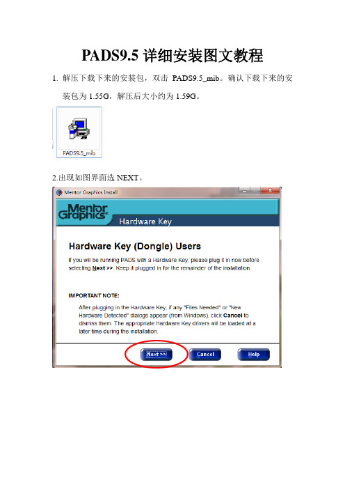
PADS9.5详细安装图文教程
1.解压下载下来的安装包,双击PADS9.5_mib。
确认下载下来的安
装包为1.55G,解压后大小约为1.59G。
2.出现如图界面选NEXT。
3.出现如下界面,点Skip。
4.出现如图界面,点Agree。
5.出现如下界面,选Modify。
6.出现如下界面,在Product Selection选项处选择自已需要安装的组件,一般单机版,不选择最后一项,最后点Done。
7.出现如下界面点Install。
8.出现如下界面,耐心等待。
9.出现以下界面,选择at a later time,并点击Done。
10.运行我提供的和谐文件“Crack”,自动进行破解,2-3分钟后再打开软件即可。
注:不能在打开软件的状态下运行破解。
Crack双击后无任何反应,只需等待几分钟再打开软件即可。
PADS9.3安装教程
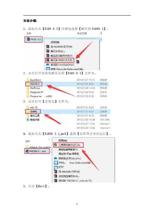
安装步骤:1、鼠标右击【PADS9.3】压缩包选择【解压到PADS9.3】。
2、双击打开安装包解压后的【PADS9.3】文件夹。
3、双击打开【安装包】文件夹。
4、鼠标右击【PADS9.3.1_mib】选择【以管理员身份运行】。
5、点击【Next】。
6、点击【Skip】。
7、点击【Agree】。
8、点击【Modify】。
9、选择【Product Selection】,取消勾选【Server Services】。
10、选择【Target Path】,点击【Browse】更改软件的安装路径,建议安装在除C盘之外的其它的磁盘,可以在D盘或者其它磁盘新建一个【PADS9.3】文件夹,然后点击【Done】。
11、点击【Install】。
12、软件安装中(大约需要20分钟)。
13、选择【at a later time】,然后点击【Done】。
件夹。
15、鼠标右击【MentorKG】选择【复制】。
16、打开软件安装路径(软件安装路径为第10步设置的路径,这里为D:\PADS 9.3),然后鼠标右击空白处选择【粘贴】。
17、鼠标右击【MentorKG】选择【以管理员身份运行】。
18、出现显示框后,点击键盘上的【Enter】键。
19、出现【LICENSE】记事本后,点击【文件】,选择【另存为】。
20、保存到软件的安装路径下(软件安装路径为第10步设置的路径,这里为D:\PADS9.3),保存为【LICENSE.TXT】,然后点击【保存】。
设置】,然后选择【高级】,然后点击【环境变量】。
22、点击【新建】,新建一个用户变量。
23、变量名:【MGLS_LICENSE_FILE】,变量值为刚刚保存的【LICENSE.TXT】路径,然后点击【确定】。
24、出现新建的变量名后点击【确定】。
25、双击打开安装包解压后的【PADS9.3】文件夹里面的【win10】文件夹。
26、选择【chs】和【enu】文件夹,鼠标右击选择【复制】。
InstallingOrCAD9.2安装破解说明

InstallingOrCAD9.2安装破解说明Installing OrCAD 9.2(1)Disable Anti-virus programs(2)Run the program setup.exeLicensing(3)Choose: StandaloneInstall Product on Standalone Computer(4)Enter the key Codes:BFIK(5)Enter the authorization code: 12345(6)Click YES to override all .dll files and extensions(7)Finish installation(8)Run PDXOrCAD.exe from the CD under the Crack\ folder(9)Brows for C:\Program Files\Orcad in the tab shown(10)Click Apply then ByeByeDrawing Circuits (Capture CIS)A. Start a new Project(1)Run “Capture CIS” from the Start menu(2)Run: File ? New ? Projecti.Write a Nameii.Choose Analog or Mixed A/Diii.Brows a location under My Documents\iv.Click Nextv.Choose “Create a blank project”(3)A blank page named “SCHEMATIC1” is createdB. Add Libraries(1)Click on the blank sheet(2)Run: Place ? Part or click on the icon on the right panel(3)Click Add Library(4)You need, at least, the following libraries from the directory:C:\Program Files\Orcad\Capture\Library\PSpice\ analog.olb for resistors, capacitors, and coils source.olb for voltage and current sources diode.olb for diodesbipolar.olb for BJT transistorsC. Draw Circuits(1)Place ? Part or clicki.VSIN from Source LibraryLibraryDiodeii.1N4376 fromLibraryiii.R fromAnalog(2)Press Esc after placing a part to place other types(3)Press “R” while placing a part to rotate it(4)Double click on the part value to edit their values VSIN: VOFF=0, VAMPL=1, FREQ=1000(5)Place ? Ground or click and add “0/SOURCE”(6)Place ? Wire or clickVAMPL = 1VOFF = 0D1VD. SimulationsOn the nodes you need to simulate, run:(1) PSpice ? Markers ? Voltage Level or click (2) Place these probes on every node you want (3) Run PSpice ? New Simulation Profile (4) Write a Name and click Create(5) In the simulation window (Analysis tab) choose:Analysis Type: Time Domain (Transient) Options: General SettingsRun to Time: 5ms(6) Run the simulation by: PSpice ? Run or click or press F11(7) To change the simulation end time, click PSpice ? Edit Simulation Profile (8) To make a smoother simulation, assign the “Maximum Step Size” = 1usExercise : Build the following amplifier and check that its voltage gain is about -100 V/V.VOFF = 0PCB Layout (Layout Plus)A. Inserting Test PointsWhen producing the PCB layout, all the input voltage and current sources including the ground point will not be part of the components placed in the layout. In fact, we need to place some pins in the layout to later connect to them from outside the PCB. Thus, we need to add these ports or test points in the design before generating the layout netlist:(1)Inside the CIS, add the libraryC:\Program Files\Orcad\Capture\Library\Connector.olb(2)Place a “TEST POINT” from this library on every input or output port of yourdesign.(3)Note: a warning will be given when you try to simulate your design, since Spicedoes not recognize this component. However, the simulation will run correctly.B. Generate Layout Netlist(1)Inside the CIS after you are done with the schematic, click on the project windowto highlight it(2)Under the Design Resources, highlight your project xxx.dsn object(3)Now, run Tools ? Create Netlist(4)In the new window, select the Tab “Layout” and press OK(5)Under the Output object, a file with extension .mnl is generatedC. Layout Technology(1)Start the program: “Layout Plus”(2)Run File ? New(3)Choose the default technology file under:C:\Program Files\Orcad\Layout_Plus\Data\DEFALUT.TCH(4)You will be asked to load the .mnl netlist you generated, brows it(5)Now save this work under the same project directory(6)The components and their connections will be loaded one by oneD. FootprintsSome of the components already have their footprints assigned in the original library, e.g. all PSpice libraries. For the TEST POINTS, you might need to assign footprints to them. If any component has no footprint assigned, this window will appear:(1)Click “Link existing footprint to component” button(2)You will have different libraries and different footprints exist(3)For TEST POINTS, choose LAYOUT library(4)Then choose “TP” form the list below and click OK(5)Repeat this procedure for every unassigned componentResistors & Capacitors Footprints(6)For resistors, highlight the component and right click to edit its property to assignthe AX/R05 footprint (the ? Watt) from the Axial library TM_AXIAL(7)For ceramic capacitors, select from the TM_CYLND for cylindrical capacitors orTM_CAP for ceramic capacitors(8)Always print the footprint for your layout on a paper and match physically withyour components before final PCB printingE. Assigning LayersNot all layers are needed when routing the PCB. Thus, you should only keep the following layers: TOP, BOTTOM, and DRILL. To do so:(1)Run: Tools ? Layer ? Select From Spreadsheet(2)In the shown table, double click on the Layer Type for the unwanted layers andchoose Unused.(3)Make sure the layers TOP and BOTTOM are of type Routing and the DRILL is oftype Drill(4)Close the table(5)Run: Options ? System Settings and choose Millimeters as the Display UnitsF. Define the Routing AreaYou need to define the area where you want to draw your PCB:(1)Select the Yellow layer named Global Layer(2)Run: Tools ? Obstacle ? Select Tool(3)Start drawing the area you want and watch for its size on the dimension scale onthe bottom of the screen(4)Once you finish drawing the PCB area, press ESC to exit the modeE. Placing & Routing(1)To move and place the components, make sure this button is pressed, or run:Tools ? Component ? Select Tool(2)Click the component and drag it then click again to place it.(3)Press “R” while dragging the component to rotate it.(4)Run: Auto ? Autoroute ? Board to automatically route the PCB(5)Zoom in to view the layout(6)You may replace the component again, but first Unroute the board.F. Gerber OutputsTo be able to print your layout, this layout needs to be produced in Gerber format. Before running the process, make sure that the Place Grid size is 2.0 instead of 1.27:(1)Click: Options?System Settings(2)Change Place Gird to: 2.0(3)Click: Auto ? Run Post ProcessorOther details will be announced when printing your project with other teams’ layouts in one board.File ? import ? LMD then locate the board press All+ ? start。
Win7下安装PADS9详解
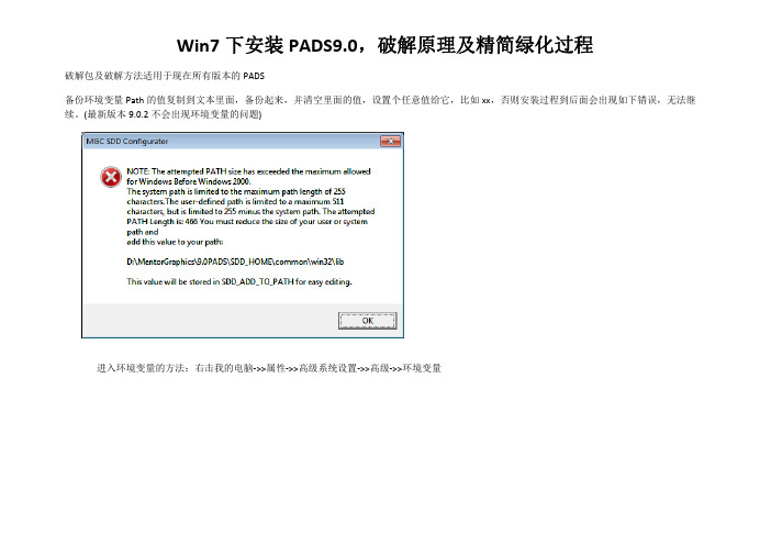
Win7下安装PADS9.0,破解原理及精简绿化过程破解包及破解方法适用于现在所有版本的PADS备份环境变量Path的值复制到文本里面,备份起来,并清空里面的值,设置个任意值给它,比如xx,否则安装过程到后面会出现如下错误,无法继续。
(最新版本9.0.2不会出现环境变量的问题)进入环境变量的方法:右击我的电脑‐>>属性‐>>高级系统设置‐>>高级‐>>环境变量开始安装:出现如下错误,意思是“无法为Mentor安装程序创建开始菜单”,点OK。
接着程序会发生如下错误退出。
没有关系,点关闭程序退出。
出现license选择窗口,如下图所示,点击选择最下面一项,即不设置license,再选Next设置工作路径,可以点Browse…自己设置路径Next, 再次出现如下错误,没关系点OK。
出现Instller.exe程序出错的窗口,点“关闭程序”。
到C:\MentorGraphics\Install目录下,可以找到installer.exe运行它,开始安装。
出现大家熟悉的窗口了哦,点Install ProductsNext, Agree, 出现路径选择窗口,强烈建议大家,不要把程序安装在C盘面,我装到D盘下。
选择组件,Next, Install开始安装了如果Path没有设置就会出现如下错误,意思是path变量值被限制在255字符,程序修改后的长度为466个字符,要减小path值的长度,安装无法成功没关系,可以重新启动配置程序,这个窗口告诉我们,可以在路径D:\MentorGraphics\win32\configurato.exe中重新启动配置程序点OK,出现如下窗口,点Done关掉就好按照第一步中的方法,清空Path的值,随便给它个值比如xx,点OK,让值设置有效。
再次运行配置程序。
运行配置程序,等一会儿后,出现如下窗口,要设置License的,不要设置,直接关闭,或点Cancel。
PADS9.3安装方法及新功能介绍_
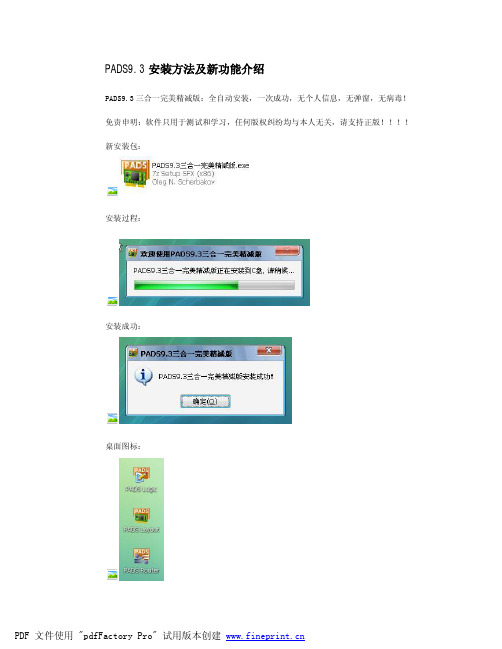
PADS9.3安装方法及新功能介绍PADS9.3三合一完美精减版:全自动安装,一次成功,无个人信息,无弹窗,无病毒!免责申明:软件只用于测试和学习,任何版权纠纷均与本人无关,请支持正版!!!!新安装包:安装过程:安装成功:桌面图标:开始菜单:安装过程中杀毒软件出现提示: 1.允许程序的所有操作:2.保留图标,不处理!(全选)CAMCAD在C:\MentorGraphics\9.3PADS\SDD_HOME\CAMCAD\CAMCADPro.EXE安装三分钟左右,在 Windows XP ; Windows 7 测试通过,请先解压,杀毒,安装!安装卸载说明:1. 卸载:删除桌面图标,开始菜单目录,C:\ flexlm;MentorGraphics;PADS Projects2. 新装:按照(1. 卸载)的方法,删除后,即可以全新安装,已经过反复测试,OK3. 修复:如果丢失了文件,可以进行修复安装,不会替换已有的文件,保留设置参数(2011-03-18修正PADS Layout首次打开,原点没有自动居中,追求打开软件第一感)PADS9.3三合一完美精减版ZERO.rar 文件大小:137.56MBSHA1:D73F67F079AE7E55BAC3B0881A7F08F85945EC50PADS9.3新增功能介绍Mentor Graphics 是电子设计自动化技术的领导产商,它提供完整的软件和硬件设计解决方案,让客户能在短时间内,以最低的成本,在市场上推出功能强大的电子产品。
当今电路板与半导体元件变得更加复杂,并随着深亚微米工艺技术在系统单芯片设计深入应用,要把一个具有创意的想法转换成市场上的产品,其中的困难度已大幅增加;为此Mentor提供了技术创新的产品与完整解决方案,让工程师得以克服他们所面临的设计挑战。
PADS软件更新的真够快啊。
PADS9.2才没多久,今年年初PADS9.3网上就有破解版下载了,看软件版本号是2011年1月8号的。
Weblogic 9.2 安装(Install Setup)的安装配置步骤

Weblogic 9.2 安装(Install Setup)的安装配置步骤2008-11-27今天用tomcat发布程序突然出现错误,试了很多办法,还是不行,后来突然想起来了Weblogic,一直想试试,但是没有机会,看来这次机会来了!翻箱倒柜终于找到了Weblogic7 8 9三个版本,呵呵,这个可是以前有机会的时候藏起来的,哈哈,安装一切顺利,运行居然报错,怎么回事呢?问了问google发现7和8用的都是 jdk1.4,而我用的是jdk1.5写的,也许这个是主要错误的问题吧,删吧,唉,再等10分钟,终于把9上装上了,哈哈,这回应该可以了吧,恩,调了个程序,可以用,看来Bea果真名不虚传啊,有点喜欢用这个东西了,以后就暂时告别小猫咪吧,把我今天配置的9拿来给大家分享下。
1、配置 WebLogic 9.2安装 WebLogic 比较容易,在这里就不再累述了,大家可以参阅相关文档。
现在着重讲一下 WebLogic 的配置,因为后面在配置MyEclipse 时将用到这里的配置信息。
①运行开始 -> 程序 -> BEA Products -> Tools -> Configuration Wizard。
②选择 Create a new WebLogic domain,Next。
③在 Select Domain Source 界面保持默认,Next。
④在 User name 处输入 user,两个 password 都输入 12345678(密码要求 8 位),Next。
⑤在 Configure Server Start Mode and JDK 界面中保持默认,即 JDK 选择的是“Sun SDK 1.5.0_04 @ C:\BEA\jdk150_04”,注意这里若选择“Other JDK”配置比 SDK 1.5.0_04 更高的版本,服务器启动时将会出现异常,所以最好保持默认,然后 Next。
PADS使用技巧

PADS软件是MentorGraphics公司的电路原理图和PCB设计工具软件。
目前该软件是国内从事电路设计的工程师和技术人员主要使用的电路设计软件之一,是PCB设计高端用户最常用的工具软件。
按时间先后:powerpcb----PADS2005----PADS2007----PADS9.0----PADS9.1----PADS9.2----PADS9.3——PADS9.4……,没有PADS2009。
2012-10-18发布PADS9.5Mentor Graphics公司的PADS Layout/Router环境作为业界主流的PCB设计平台,以其强大的交互式布局布线功能和易学易用等特点,在通信、半导体、消费电子、医疗电子等当前最活跃的工业领域得到了广泛的应用。
PADS Layout/ Router支持完整的PCB设计流程,涵盖了从原理图网表导入,规则驱动下的交互式布局布线,DRC/DFT/DFM校验与分析,直到最后的生产文件(Gerber)、装配文件及物料清单(BOM)输出等全方位的功能需求,确保PCB 工程师高效率地完成设计任务。
PADS2005sp2:稳定性比较好,但是很多新功能都没有;PADS2007:相比05增加了一些功能,比如能够在PCB中显示器件的管脚号,操作习惯也发生了一些变化;PADS9.2:相比以前的版本增加了一些比较重要的功能,比如能在PCB中显示Pad、Trace 和Via的网络名,能够在Layout和Router之间快速切换等等,非常好用。
还有,最重要的一点是:支持win7系统。
目前大多工程师使用的是PADS2007,同时Pads实现了从高版本向低版本的兼容,例如为了解决PADS2005能打开PADS2007的工程文件:PADS9.5加入了简体中文,虚拟管脚,底层视图(翻板)等功能可以在pads2007中保存为低版本的第一步:打开pads2007绘好的原理图档案,然后单击file/EXPORT选择要保存目标点击保存,再出现AscII OUTPUT 对话里点击select all,在output formats选择pads logic 2005 击ok第二步;开启pads logic 2005 点击file/inport选择打开刚刚导出文件就ok。
weblogic9.2安装部署步骤(截图)
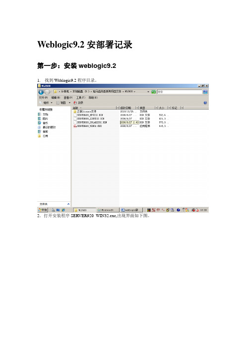
Weblogic9.2安部署记录第一步:安装weblogic9.21.找到Weblogic9.2程序目录。
2.打开安装程序SERVER920_WIN32.exe,出现界面如下图。
3.初始化完成后,点击next,所示。
图3 初始化完成后界面5 选择安装目录为d:\bea点击next.6点击next,在下图中选择complete.7.点击next.8.点击next,在下图中选择yes。
9.继续点击next后界面如下图。
10.在上图中使用默认设置,点击next。
11.点击next后开始安装。
12.点击Done。
13.点击Start WebLogic Server 9.2.14.15. 成功启动后自动弹出如下页面。
测试安装成功方法,访问http://127.0.0.1:7001/index.jsp。
http://127.0.0.1:7001/console/login/LoginForm.jsp 16.默认登录名和密码:weblogic/weblogic.1.创建域2.选择create a new weblogic domain34567910启动刚配置的域中的服务打开浏览器,输入地址http://127.0.0.1:7001/console后出现如下页面输入用户名密码:weblogic/11111111进入页面表明配置正确,启动正常。
第三步:修改端口7001为8012 依次点击base_domain->Enviroment->servers出现如下界面3 点击AdminServer(admin)4 将上图中的7001改为80,然后点击界面最下方的save按钮。
5 激活修改。
第四步:配置数据源1依次点击base_domain->Services->JDBC->Data Sources出现如下界面2 点击new按钮,出现如下界面3 选择正确的数据库类型和数据库驱动,然后点击next。