AK4399中文资料
AK47简介

AK47简介苏联著名枪械设计师米哈伊尔·季莫费耶维奇·卡拉什尼科夫成名之作。
俄语全称为АвтоматКалашниковаобразца1947 года,A是俄语里自动步枪的第一个字母,K则是卡拉什尼科夫名字的第一个字母,47是出厂年份,意为“卡拉什尼科夫1947年定型的自动步枪”。
关于读音:北约读音为英文AK。
在俄语读音中读阿卡,是因为俄语全称为АвтоматКалашниковаобразца1947 года,“阿”取自Автомат的A,“卡”取自Калашникова的K, 但是“Ka”才发音为“卡”,简称AK只是单单一个“K”,不用附带“a”来读。
所以英文读音AK没有错误;俄语读音阿卡,也可以,这算是俄式简称,但是使用俄语读音时,枪的全称必须写成和读成俄式名字АвтоматКалашниковаобразца1947 года,而不能采用英文名称。
相比第二次世界大战时期的步枪,AK-47突击步枪枪身短小、射程较短,适合较近距离的战斗。
自动方式是枪管短后座式。
回转式闭锁枪机。
7.62毫米口径,发射7.62×39毫米M1943型中间型威力枪弹,容量30发子弹的弧形弹匣供弹,后备弹夹最多可带90发子弹,相当于3个弹夹。
可选择半自动或全自动的发射方式。
1947年被选定为苏联军队制式装备,1949年最终定型,正式投入量产,伊热夫斯克军工厂负责生产。
1951年开始装备苏军。
1953年改变了机匣的生产方法,变冲压工艺为机加工艺,随即开始大量装备。
苏军摩托化步兵、空军和海军的警卫、勤务人员使用木制或塑料制固定枪托型,АKС-47(英文AKS-47)采用可折叠金属枪托的型号。
枪托折叠长645毫米。
供空降兵、坦克兵和特种兵使用。
有一些说法称卡拉什尼科夫借鉴了如下枪的设计:布尔基纳的TKB-415 ,AS-44或是西蒙诺夫的AVS-31。
Gordon Williamson甚至说STG-44影响了AK-47,这说法当然不可信但至少有证据表明雨果-施梅瑟,战后“协助”过卡氏的工作。
AK-47枪王之王
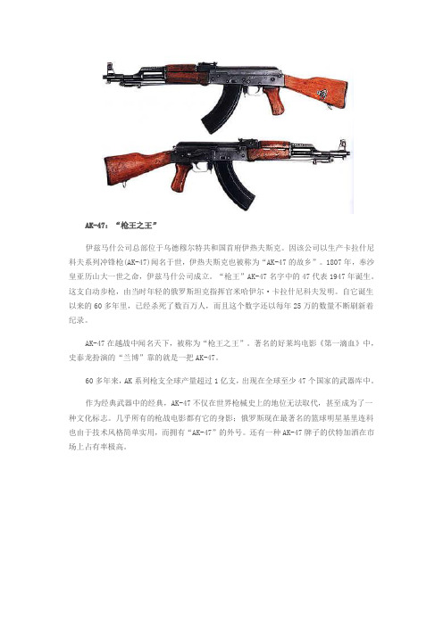
AK-47:“枪王之王”
伊兹马什公司总部位于乌德穆尔特共和国首府伊热夫斯克。
因该公司以生产卡拉什尼科夫系列冲锋枪(AK-47)闻名于世,伊热夫斯克也被称为“AK-47的故乡”。
1807年,奉沙皇亚历山大一世之命,伊兹马什公司成立。
“枪王”AK-47名字中的47代表1947年诞生。
这支自动步枪,由当时年轻的俄罗斯坦克指挥官米哈伊尔·卡拉什尼科夫发明。
自它诞生以来的60多年里,已经杀死了数百万人,而且这个数字还以每年25万的数量不断刷新着纪录。
AK-47在越战中闻名天下,被称为“枪王之王”。
著名的好莱坞电影《第一滴血》中,史泰龙扮演的“兰博”靠的就是一把AK-47。
60多年来,AK系列枪支全球产量超过1亿支,出现在全球至少47个国家的武器库中。
作为经典武器中的经典,AK-47不仅在世界枪械史上的地位无法取代,甚至成为了一种文化标志。
几乎所有的枪战电影都有它的身影;俄罗斯现在最著名的篮球明星基里连科也由于技术风格简单实用,而拥有“AK-47”的外号。
还有一种AK-47牌子的伏特加酒在市场上占有率极高。
《战地:叛逆连队2》全武器、装备、专长解锁简介
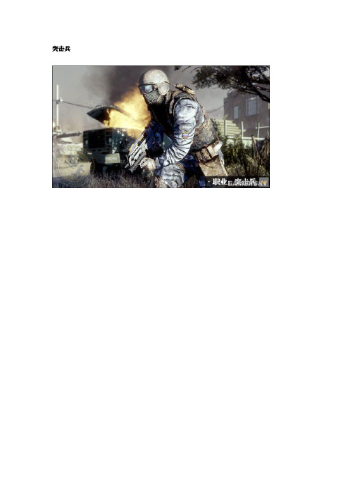
突击兵解锁要求图主武器:AEK-971 Vintovka俄军标准配置突击步枪。
AEK971的开发初衷是在全自动射击的同时保持射击精度。
全自动,威力较低,射速较高。
*(1)XM8 Prototype美军试作型突击步枪。
多功能的XM8能让使用者在前线高速完成维修及装配动作。
全自动,威力较高,射速中等。
F2000 Assualt一件比利时产的全自动突击步枪。
无托式的枪身能支持多种瞄准镜与挂件,使其能胜任任何任务需要。
全自动,威力低,射速高。
Stg .77 AUG一件表现突出、耐性良好的奥地利产突击步枪。
高机动性决定了她杰出的近战能力。
全自动,威力较高,射速较低。
AN-94 Abakan俄军特种部队配枪。
致死力,停止力,穿甲能力高。
二发点射,威力高,射速低。
HK416(游戏中显示为M416,其实型号应该是HK416)德国产突击步枪。
是日益过时的M4/M16的改良版本。
相比M4,故障率大大下降。
全自动,威力较高,射速较低。
M16A2美国陆军的象征。
M16A2的开发初衷是节省弹药,提升射击精度与威力。
三发点射,威力较低,射速较高。
装备1:*(2)C4 Explosive【C4塑胶炸药】默认携弹量:3布置上限:6*(3)俗称C4,是突击兵装备通用枪械时的配套装备。
默认LB(360)/ L1(PS3)布置,RB/ R1引爆。
可粘附在载具与建筑物上。
威力巨大,两枚可废掉一辆坦克。
另外,C4可以通过射击、使用爆炸物等手段,手动引爆。
40MM Grenade【40MM 高爆榴弹】默认携弹量:1/1俗称榴弹。
在突击步枪上装备榴弹发射组件。
直击步兵目标能产生秒杀效果。
拆墙便利,可视作开门钥匙。
40MM Smoke Launcher【40MM烟雾弹】默认携弹量:1/1俗称烟雾弹。
在突击步枪上装备烟雾弹发射组件。
使用后能产生烟雾。
烟雾范围不大、掩护效果一般。
若是在烟雾范围内的我方单位已被敌军标记/报点,则标记/报点失效。
未被标记/报点的我方单位在一定时间内对标记/报点免疫。
CSOL武器代码
musket 神怒之炎
p228 P228
p90 P90
p90lapin 兔耳P90
pkm 裁决者PKM
poisongun 腐蚀烈焰
k1ase K1A SE
k3 K3
kingcobra 眼镜王蛇(Kingcobra)
kingcobrag 帝皇眼镜王蛇
knife 海豹短刀
kriss 致命蝎刺
ksg12 灼热剃刀KSG12
qbarrel 破碎炙炎EX(女英雄枪)
qbb95 QBB95
qbb95EX QBB95·暴龙
qbz95b QBZ95B
rainbowgun 画梅
scarA SCAR
scarH SCAR(强化版)(30发子弹)
elite Elites
ethereal 尘埃之光
f2000 F2000
famas Famas
fglauncher 礼花发射器
firecracker 高爆手雷
fiveseven FiveSeven flamethrower 焚烬者Salamander
usas12 USAS12
usas12camo 迷彩USAS12
usp USP45
uspred USP45(深红)
uts15 爆炎剃刀UTS15
violingun D小调协奏曲
vsk94 VSK94
akm AKM
an94 AN94
anaconda 左轮军魂(Anaconda)
as50 末日骑士AS50
as50g 末日金骑
at4 AT-Lance火箭发射器
AK大神中文字幕教程
【虚拟之光分享】-VC--85.rar
/file/c2u16rth#
【虚拟之光分享】-VC-86._Fracture_Design.rmvb
/file/be6kvwwa#
【虚拟之光分享】videocopilot系列-79-Organic_Mesh.rmvb
/file/dpd8ui8b#
【虚拟之光分享】videocopilot系列-80-3D.Falloff.rar
【虚拟之光分享】videocopilot系列-94Particle.Explosion.rar
/file/be6kv9tv#
【虚拟之光分享】videocopilot系列-95.Scene.Re-Lighting.rar
/file/e73axv3p#
【虚拟之光分享】115-银河系天体视频特效教程.rar
/file/dpd8u9y1#
【虚拟之光分享】116瓦解的墙.rar
/file/dpd8u9gu#
/file/anixrld1#
【虚拟之光分享】videocopilot系列-98.Reflection_Plug-in_tut.相关插件.rar
/file/anixrrhb#
【虚拟之光分享】videocopilot系列-101.Sure.Target.rar
【虚拟之光分享】videocopilot系列-75.3D.Crater.p2.rmvb
/file/anixr46g#
【虚拟之光分享】videocopilot系列-76-3D.Crater.part3.rar
/file/anixrraw#
【虚拟之光分享】videocopilot系列-102.smoke_trails_tutorial.rmvb
cs4396技术资料

AOUTR+ AOUTR-
HARDWARE MODE CONTROL (CONTROL PORT)
VOLTAGE REFERENCE
M4 M3 M2 M1 (AD0/CS) (AD1/CDIN) (SCL/CCLK)
M0 RESET (SDA/CDOUT)
MUTEC MUTE
FILT+
VREF
FILT-
Bit Conversion l Up to 192 kHz Sample Rates l 120 dB Dynamic Range l -100 dB THD+N l Advanced Dynamic-Element Matching l Low Clock Jitter Sensitivity l Digital De-emphasis for 32 kHz, 44.1 kHz and 48 kHz l External Reference Input
I
SCLK LRCK SDATA SERIAL INTERFACE AND FORMAT SELECT SOFT MUTE DE-EMPHASIS FILTER
INTERPOLATION FILTER MCLK CLOCK DIVIDER
MULTIห้องสมุดไป่ตู้BIT ∆Σ MODULATOR
DYNAMIC ELEMENT MATCHING LOGIC
Copyright © Cirrus Logic, Inc. 1999 (All Rights Reserved)
JUL ‘99 DS288PP1 1
CS4396
TABLE OF CONTENTS
1.0 CHARACTERISTICS/SPECIFICATIONS ...................
CSGO所有枪械名称及绑定指令大全

CS:GO所有枪械名称及绑定指令大全CS:GO枪械基础绑定指令格式:bind + 键位名称+ "buy 枪械名称" (输入时无需添加"+"号)小键盘键位名称及对应键位表:kp_slash (对应键位 "/")kp_multiply (对应键位 "*")kp_minus (对应键位"-")kp_home (对应键位 "7")kp_uparrow (对应键位 "8")kp_pgup (对应键位 "9")kp_leftarrow (对应键位 "4")kp_5 (对应键位 "5")kp_rightarrow (对应键位 "6")kp_end (对应键位 "1")kp_downarrow (对应键位 "2")kp_pgdn (对应键位 "3")kp_ins (对应键位 "0")kp_del (对应键位 ".")kp_plus (对应键位"+")kp_enter (对应键位 "Enter")CS:GO枪械名称大全(括号里为控制台应枪械名称)Scout (ssg08)Galil (galilar)Famas (famas)SG550 (sg550)AUG (aug)M4 (m4a1)AK47 (ak47)T专用步枪(g3sg1)CT专用步枪(scar20)AWP (awp)Mac 10 (mac10)UMP (ump45)P90 (p90)Bizon (bizon)MP7 (mp7)MP9 (mp9)Auto Shotgun (xm1014)Mag7 (mag7)Sawed Off Shotgun (sawedoff) Nova Shotgun (nova)M249 (m249)Negev (negev)228 Compact (p228)Glock (glock)Dual Elites (elite)Five Seven (fiveseven)Desert Eagle (deagle)Tec9 (tec9)HKP2000 (hkp2000)P250 (p250)Incendiary Grenade (incgrenade) Flashbang (flashbang)Smoke (smokegrenade)HE Grenade (hegrenade) Molotov (molotov)Decoy (decoy)Kevlar (kevlar)Kevlar+Helmet (vesthelm)Zeus x27 (taser)Defuse Kit (defuser)CS:GO枪械绑定指令示范:bind f1 “buy ak47; buy m4a1; buy vesthelm; buy deagle; buy flashbang; buy smokegrenade; buy molotov; buy incgrenade; buy defuser”bind f2 “buy awp; buy vesthelm; buy deagle; buy flashbang; buy smokegrenade; buy molotov; buy incgrenade; buy defuser”bind f3 “buy vesthelm”bind f4 “buy kevlar”bind f5 “buy hegrenade”bind f6 “buy flashbang”bind f7 “buy smokegrenade”bind f8 “buy molotov; buy incgrenade”bind kp_home “buy awp”bind kp_uparrow “buy g3sg1; buy scar20″bind kp_pgup “buy ssg08″bind kp_leftarrow “buy ak47; buy m4a1″bind kp_5 “buy sg556; buy aug”bind kp_rightarrow “buy galilar; buy famas”bind kp_end “buy p90″bind kp_downarrow “buy bizon”bind kp_pgdn “buy mac10; buy mp9″bind kp_minus “buy deagle”bind kp_plus “buy tec9″bind kp_enter “buy p250″bind kp_ins “buy defuser”以上所有枪械绑定指令需保存在config.cfg中,即:Steam/Steamapps/Common/Counter-Strike Global Offensive/csgo/cfg/config.cfg使用小技巧:bind b "buymenu; buy defuser" - 在打开购买菜单时,自动购买钳子(拆弹器)—— CT 专用bind f1 "toggle sensitivity 1 5" - 按下F1键,可以将鼠标灵敏度自动调整到5,再按一次则还原到1(灵敏度大小可自行设置)bind kp_enter "use weapon_flashbang" - 快速使用闪光弹。
AK4396中文资料

ASAHI KASEI [AKD4396-SBW]AKD4396-SBWEvaluation boardGeneral DescriptionThe AKD4396-SBW is an evaluation board for AK4396, which is 192kHz sampling 24Bit ∆Σ DAC. The AKD4396-SBW includes a LPF which can add differential analog outputs from the AK4396 and also has a digital interface. Therefore, it is easy to evaluate the AK4396.Ordering GuideAKD4396-SBW --- Evaluation board for AK4396FunctionOn-board Analog output buffer circuitOn-board digital audio interface. (AK4113)Figure 1 Block diagram* Circuit diagram and PCB layout are attached at the end of this manual.COAX is recommended for an evaluation of the Sound quality.ASAHI KASEI [AKD4396-SBW]Operation sequence1) Set up the power supply lines. (See “Other jumpers set-up”.)Name Color Voltage Comments Attention+15V Red +12∼+15V Regulator,Power supply for Op-amp.This jack is always needed. Power line-15V Blue -12∼-15V Regulator,Power supply for Op-amp.This jack is always needed. Power lineAGND Black 0V GND This jack is always needed.Table 1 Set up of power supply linesEach supply line should be distributed from the power supply unit.2) Set-up the jumper pins3) Set-up the DIP switches. (See the followings.)4) Power onThe AK4396 should be reset once bringing SW1 (PDN) “L” upon power-up.ASAHI KASEI [AKD4396-SBW]Evaluation mode1. DIR(COAX) (default)J1 is used for the evaluation using such as CD test disk. The DIR generates MCLK, BICK and LRCK SDATA from the received data through BNC connector (J1). Setting of jumper is shown below.COAX is recommended for an evaluation of the Sound quality.JP1OPT COAXBNC (Default)Figure 2 Jumper setting, when using DIR2. DIR(Optical Link)PORT1 is used for the evaluation using such as CD test disk. The DIR generates MCLK, BICK and LRCK SDATA from the received data through optical connector (PORT2: TORX176). Setting of jumper is shown below.JP1OPT COAXPORT2Figure 3 Jumper setting, when using DIR3. All clocks are fed through the PORT1.-R9, R12, R13, R14 : open-R10, R15, R19, R20 : 100Ω or short (0 Ω)DIP Switch setting[SW2]: AK4113 settingNo. Pin OFFONDefault 1 OCKS1ON2 OCKS0AK4113 Master Clock setting Refer to Table4OFFTable 2 SW2 setting[SW3]: AK4396 settingNo. PinOFFONDefault1- 2 P/S Serial mode (Note) Parallel modeONNote : When using the serial mode, R5 and R17 should be removed.Table 3 SW3 settingASAHI KASEI [AKD4396-SBW]The frequency of the master clock output is set by OCKS0 and OCKS1 as shown in Table 4.FrequencyOCKS1 OCKS0 MCLK@fs=88.2/96kHz0 0 256fs@32/44.1/48kHz1 0 512fsDefault1 1 128fs@176.4/192kHzTable 4 MCLK ClockSW1 setting[SW1](PDN): Reset of AK4396. Select “H” during operation.External Analog CircuitThe differential output circuit and LPF is implemented on board. The differential outputs of AK4396 is buffered by non-inverted circuit(2nd order LPF, fc=182k, Q=0.637, G=+3.9dB). LPF adds differential outputs(1st order LPF, fc=284k, G=-0.84dB). NJM5534D is used for op-amp on this board that has low noise and high voltage torelance characteristics. Analog signal is output via BNC connectors on the board. The output level is about 2.8Vrms (typ@VREF=5.0V) by BNC.Figure 4External Analog Filter40kHz (Double)80kHz (quad)AKD4396-SBWFilterInternal Filter -0.3dB -1dBExternal LPF -0.19dB -0.85dBTotal -0.49dB -1.85dBThis table shows typical value.Table 5 Frequency ResponsesASAHI KASEI [AKD4396-SBW]2. Control Software ManualSet-up of evaluation board and control software1. Set up the AKD4396-SBW according to previous term.2. Connect IBM-AT compatible PC with AKD4396-SBW by 10-line type flat cable (packed with AKD4396-SBW).Take care of the direction of 10pin header. (Please install the driver in the CD-ROM when this control software is used on Windows 2000/XP. Please refer “Installation Manual of Control Software Driver by AKM device control software”. In case of Windows95/98/ME, this installation is not needed. This control software does not operate on Windows NT.)3. Insert the CD-ROM labeled “AKD4396-SBW Evaluation Kit” into the CD-ROM drive.4. Access the CD-ROM drive and double-click the icon of “akd4396.exe” to set up the control program.5. Then please evaluate according to the follows.Operation flowKeep the following flow.1. Set up the control program according to explanation above.2. Click “Port Reset” button.Explanation of each buttons1. [Port Reset] : Set up the USB interface board (AKDUSBIF-A) .2. [Write default] : Initialize the register of AK4396.3. [All Write] : Write all registers that is currently displayed.4. [Function1] : Dialog to write data by keyboard operation.5. [Function2] : Dialog to write data by keyboard operation.6. [Function3] : The sequence of register setting can be set and executed.7. [Function4] : The sequence that is created on [Function3] can be assigned to buttons andexecuted.8. [Function5]: The register setting that is created by [SAVE] function on main window canbe assigned to buttons and executed.9. [SAVE] : Save the current register setting.10. [OPEN] : Write the saved values to all register.11. [Write] : Dialog to write data by mouse operation.Indication of dataInput data is indicated on the register map. Red letter indicates “H” or “1” and blue one indicates “L” or “0”. Blank is the part that is not defined in the datasheet.ASAHI KASEI [AKD4396-SBW] Explanation of each dialog1. [Write Dialog]: Dialog to write data by mouse operationThere are dialogs corresponding to each register.Click the [Write] button corresponding to each register to set up the dialog. If you check the check box, databecomes “H” or “1”. If not, “L” or “0”.If you want to write the input data to AK4396, click [OK] button. If not, click [Cancel] button.2. [Function1 Dialog] : Dialog to write data by keyboard operationAddress Box: Input registers address in 2 figures of hexadecimal.Data Box: Input registers data in 2 figures of hexadecimal.If you want to write the input data to AK4396, click [OK] button. If not, click [Cancel] button.3. [Function2 Dialog] : Dialog to evaluate ATTAddress Box: Input registers address in 2 figures of hexadecimal.Start Data Box: Input starts data in 2 figures of hexadecimal.End Data Box: Input end data in 2 figures of hexadecimal.Interval Box: Data is written to AK4642 by this interval.Step Box: Data changes by this step.Mode Select Box:If you check this check box, data reaches end data, and returns to start data.[Example] Start Data = 00, End Data = 09Data flow: 00 01 02 03 04 05 06 07 08 09 09 08 07 06 05 04 03 02 01 00If you do not check this check box, data reaches end data, but does not return to start data.[Example] Start Data = 00, End Data = 09Data flow: 00 01 02 03 04 05 06 07 08 09If you want to write the input data to AK4396, click [OK] button. If not, click [Cancel] button.ASAHI KASEI [AKD4396-SBW] 4. [Save] and [Open]4-1. [Save]Save the current register setting data. The extension of file name is “akr”.(Operation flow)(1) Click [Save] Button.(2) Set the file name and push [Save] Button. The extension of file name is “akr”.4-2. [Open]The register setting data saved by [Save] is written to AK4396. The file type is the same as [Save]. (Operation flow)(1) Click [Open] Button.(2) Select the file (*.akr) and Click [Open] Button.ASAHI KASEI [AKD4396-SBW]5. [Function3 Dialog]The sequence of register setting can be set and executed.(1) Click [F3] Button.(2) Set the control sequence.Set the address, Data and Interval time. Set “-1” to the address of the step where the sequence should be paused. (3) Click [Start] button. Then this sequence is executed.The sequence is paused at the step of Interval="-1". Click [START] button, the sequence restarts from the paused step. This sequence can be saved and opened by [Save] and [Open] button on the Function3 window. The extension of file name is “aks”.Figure 5. Window of [F3]ASAHI KASEI [AKD4396-SBW] 6. [Function4 Dialog]The sequence that is created on [Function3] can be assigned to buttons and executed. When [F4] button is clicked, the window as shown in Figure 6 opens.Figure 6. [F4] windowASAHI KASEI [AKD4396-SBW]6-1. [OPEN] buttons on left side and [START] buttons(1) Click [OPEN] button and select the sequence file (*.aks).The sequence file name is displayed as shown in Figure 7.Figure 7. [F4] window(2)(2) Click [START] button, then the sequence is executed.3-2. [SAVE] and [OPEN] buttons on right side[SAVE] : The sequence file names can assign be saved. The file name is *.ak4.[OPEN] : The sequence file names assign that are saved in *.ak4 are loaded.3-3. Note(1) This function doesn't support the pause function of sequence function.(2) All files need to be in same folder used by [SAVE] and [OPEN] function on right side.(3) When the sequence is changed in [Function3], the file should be loaded again in order to reflect the change.ASAHI KASEI [AKD4396-SBW] 7. [Function5 Dialog]The register setting that is created by [SAVE] function on main window can be assigned to buttons and executed.When [F5] button is clicked, the following window as shown in Figure 8opens.Figure 8. [F5] window7-1. [OPEN] buttons on left side and [WRITE] button(1) Click [OPEN] button and select the register setting file (*.akr).(2) Click [WRITE] button, then the register setting is executed.7-2. [SAVE] and [OPEN] buttons on right side[SAVE] : The register setting file names assign can be saved. The file name is *.ak5.[OPEN] : The register setting file names assign that are saved in *.ak5 are loaded.7-3. Note(1) All files need to be in same folder used by [SAVE] and [OPEN] function on right side.(2) When the register setting is changed by [Save] Button in main window, the file should be loaded again inorder to reflect the change.ASAHI KASEI [AKD4396-SBW]Measurement Results[Measurement condition]• Measurement unit : Audio Precision System two Cascade (AP2) • MCLK : 512fs (44.1kHz), 256fs (96kHz), 128fs (192kHz) • BICK : 64fs• fs : 44.1kHz, 96kHz, 192kHz • Bit : 24bit• Power Supply : AVDD= DVDD=5V• Interface: Internal DIR (48kHz, 96kHz, 192kHz) • Temperature: Roomfs=44.1kHzParameter Input signal Measurement filter ResultsS/(N+D) 1kHz, 0dB 20kLPF 99.4 dB DR 1kHz, -60dB 22kLPF, A-weighted 119.0 dB S/N “0” data 22kLPF, A-weighted119.0 dBfs=96kHzParameter Input signal Measurement filter ResultsS/(N+D) 1kHz, 0dB 40kLPF 99.0 dB DR 1kHz, -60dB 40kLPF 114.0 dB DR 1kHz, -60dB 22kLPF, A-weighted 119.3 dBS/N “0” data 40kLPF 114.0 dB S/N “0” data 22kLPF, A-weighted119.3 dBfs=192kHzParameter Input signal Measurement filter ResultsS/(N+D) 1kHz, 0dB 40kLPF 98.7 dB DR 1kHz, -60dB 40kLPF 111.2 dB DR 1kHz, -60dB 22kLPF, A-weighted 116.4 dBS/N “0” data 40kLPF 113.6 dB S/N “0” data 22kLPF, A-weighted119.0 dBASAHI KASEI [AKD4396-SBW]Plots(fs=44.1kHz)AKMAK4396 FFT fs=44.1kHz AVDD=DVDD=5V, 0dBFS input2020k501002005001k2k5k10kHzd B r AFigure 9 FFT (fin=1kHz, Input Level=0dBFS)AKMAK4396 FFT plot fs=44.1kHz AVDD=DVDD=5V, -60dBFS inputd B r AHzFigure 10 FFT (fin=1kHz, Input Level=-60dBFS)ASAHI KASEI [AKD4396-SBW](fs=44.1kHz)AKM AK4396 FFT plot fs=44.1kHzAVDD=DVDD=5V, No signal inputdBrA501002005001k2k5k10k 2020kHzFigure 11FFT (Noise Floor)AKM AK4396 FFT fs=44.1kHzAVDD=DVDD=5V, 0dBFS input, outband noizedBrA501002005001k2k5k10k20k50k 20100kHzFigure 12FFT (Out of band noise)ASAHI KASEI [AKD4396-SBW](fs=44.1kHz)AKMAK4396 THD+N vs Input Level fs=44.1kHzAVDD=DVDD=5V, 0dBFS-140+0-130-120-110-100-90-80-70-60-50-40-30-20-10dBFSd B r AFigure 13 THD+N vs. Input level (fin=1kHz)AKMAK4396 THD+N vs Input Frequency fs=44.1kHzAVDD=DVDD=5V, 0dBFS input2020k501002005001k 2k 5k 10kHzd B r AFigure 14 THD+N vs. Input Frequency (Input level=0dBFS)ASAHI KASEI [AKD4396-SBW](fs=44.1kHz)AKMAK4396 Linearity fs=44.1kHz AVDD=DVDD=5V, 0dBFS input-150+0-140-130-120-110-100-90-80-70-60-50-40-30-20-10dBFSd B r AFigure 15 Linearity (fin=1kHz)AKMAK4396 Frequency Respons fs=44.1kHzAVDD=DVDD=5V, 0dBFS input2k20k4k6k8k10k 12k14k16k18kHzd B r AFigure 16 Frequency Response (Input level=0dBFS)ASAHI KASEI [AKD4396-SBW](fs=44.1kHz)AKMAK4396 Crosstalk (Red:Lch, Blue:Rch) fs=44.1kHzAVDD=DVDD=5V, 0dBFS input2020k501002005001k 2k 5k 10k Hzd BFigure 17 Crosstalk (Input level=0dBFS)ASAHI KASEI [AKD4396-SBW](fs=96kHz)AKMAK4396 FFT fs=96kHz AVDD=DVDD=5V, 0dBFS input4040k501002005001k2k5k10k20kHzd B r AFigure 18 FFT (fin=1kHz, Input Level=0dBFS)AKMAK4396 FFT fs=96kHzAVDD=DVDD=5V, 0dBFS input, notch4040k501002005001k2k5k10k20kHzd B r AFigure 19 FFT(fin=1kHz, Input Level=0dBFS, Notch)ASAHI KASEI [AKD4396-SBW](fs=96kHz)AKMAK4396 FFT fs=96kHzAVDD=DVDD=5V, -60dBFS input4040k501002005001k2k 5k 10k 20k Hzd B r AFigure 20 FFT (fin=1kHz, Input Level=-60dBFS)AKMAK4396 FFT fs=96kHzAVDD=DVDD=5V, No signal inputHzd B r AFigure 21 FFT (Noise Floor)ASAHI KASEI [AKD4396-SBW](fs=96kHz)AKMAK4396 THD+N vs Input Level fs=96kHzAVDD=DVDD=5V, 0dBFS input-140+0-130-120-110-100-90-80-70-60-50-40-30-20-10dBFSd B r AFigure 22 THD+N vs. Input level (fin=1kHz)AKMAK4396 THD+N vs Input Frequency fs=96kHzAVDD=DVDD=5V, 0dBFS input4040k501002005001k2k 5k 10k 20kHzd B r AFigure 23 THD+N vs. Input Frequency (Input level=0dBFS)ASAHI KASEI [AKD4396-SBW](fs=96kHz)AKMAK4396 Linearity fs=96kHz AVDD=DVDD=5V, 0dBFS input-150+0-140-130-120-110-100-90-80-70-60-50-40-30-20-10dBFSd B r AFigure 24 Linearity (fin=1kHz)AKMAK4396 Frequency Respons fs=96kHzAVDD=DVDD=5V, 0dBFS input2.5k40k5k7.5k10k12.5k15k17.5k20k 22.5k25k27.5k30k32.5k35k37.5kHzd B r AFigure 25 Frequency Response (Input level=0dBFS)ASAHI KASEI [AKD4396-SBW](fs=96kHz)AKMAK4396 Crosstalk (Red:Lch, Blue:Rch) fs=96kHzAVDD=DVDD=5V, 0dBFS input4040k501002005001k2k 5k 10k 20k Hzd BFigure 26 Crosstalk (Input level=0dBFS)ASAHI KASEI [AKD4396-SBW](fs=192kHz)AKMAK4396 FFT fs=192kHz AVDD=DVDD=5V, 0dBFS input9080k2005001k2k5k10k20k50kHzd B r AFigure 27 FFT (fin=1kHz, Input Level=0dBFS)AKMAK4396 FFT fs=192kHzAVDD=DVDD=5V, 0dBFS input, notch9080k2005001k2k5k10k20k50kHzd B r AFigure 28 FFT(fin=1kHz, Input Level=0dBFS, Notch)ASAHI KASEI [AKD4396-SBW](fs=192kHz)AKMAK4396 FFT fs=192kHzAVDD=DVDD=5V, -60dBFS inputd B r A9080k2005001k2k5k10k20k50kHzFigure 29 FFT (fin=1kHz, Input Level=-60dBFS)AKMAK4396 FFT fs=192kHzAVDD=DVDD=5V, No signal inputd B r A9080k2005001k2k5k10k20k50kHzFigure 30 FFT (Noise Floor)ASAHI KASEI [AKD4396-SBW](fs=192kHz)AKMAK4396 THD+N vs Input Level fs=192kHzAVDD=DVDD=5V, 0dBFS input-140+0-130-120-110-100-90-80-70-60-50-40-30-20-10dBFSd B r AFigure 31 THD+N vs. Input level (fin=1kHz)AKMAK4396 THD+N vs Input Frequency fs=192kHzAVDD=DVDD=5V, 0dBFS input9080k2005001k 2k5k 10k 20k 50kHzd B r AFigure 32 THD+N vs. Input Frequency (Input level=0dBFS)ASAHI KASEI [AKD4396-SBW](fs=192kHz)AKMAK4396 Linearity fs=192kHz AVDD=DVDD=5V, 0dBFS input-150+0-140-130-120-110-100-90-80-70-60-50-40-30-20-10dBFSd B r AFigure 33 Linearity (fin=1kHz)AKMAK4396 Frequency Respons fs=192kHzAVDD=DVDD=5V, 0dBFS input5k80k10k15k20k25k30k35k40k 45k50k55k60k65k70k75kHzd B r AFigure 34 Frequency Response (Input level=0dBFS)ASAHI KASEI [AKD4396-SBW]AKMAK4396 Cross talk (Red:Lch, Blue:Rch) fs=192kHzAVDD=DVDD=5V, 0dBFS input9080k2005001k 2k5k 10k 20k 50k Hzd BFigure 35 Crosstalk (Input level=0dBFS)ASAHI KASEI [AKD4396-SBW]Revision HistoryIMPORTANT NOTICE• These products and their specifications are subject to change without notice. Before considering any use or application, consult the Asahi Kasei Microsystems Co., Ltd. (AKM) sales office or authorized distributor concerning their current status.• AKM assumes no liability for infringement of any patent, intellectual property, or other right in the application or use of any information contained herein.• Any export of these products, or devices or systems containing them, may require an export license or other official approval under the law and regulations of the country of export pertaining to customs and tariffs, currency exchange, or strategic materials.• AKM products are neither intended nor authorized for use as critical components in any safety, life support, or other hazard related device or system, and AKM assumes no responsibility relating to any such use, except with the express written consent of the Representative Director of AKM. As used here:(a) A hazard related device or system is one designed or intended for life support or maintenanceof safety or for applications in medicine, aerospace, nuclear energy, or other fields, in which its failure to function or perform may reasonably be expected to result in loss of life or in significant injury or damage to person or property.(b) A critical component is one whose failure to function or perform may reasonably be expectedto result, whether directly or indirectly, in the loss of the safety or effectiveness of the device or system containing it, and which must therefore meet very high standards of performance and reliability.• It is the responsibility of the buyer or distributor of an AKM product who distributes, disposes of, or otherwise places the product with a third party to notify that party in advance of the above content and conditions, and the buyer or distributor agrees to assume any and all responsibility and liability for and hold AKM harmless from any and all claims arising from the use of said product in the absence of such notification.Date (YY/MM/DD) Manual Revision Board Revision Reason Contents 05/03/14 KM078100 0 First edition05/03/23 KM078101 1 Modification Change of circuit 05/06/23 KM078102 2Modification Change of circuit元器件交易网元器件交易网。
- 1、下载文档前请自行甄别文档内容的完整性,平台不提供额外的编辑、内容补充、找答案等附加服务。
- 2、"仅部分预览"的文档,不可在线预览部分如存在完整性等问题,可反馈申请退款(可完整预览的文档不适用该条件!)。
- 3、如文档侵犯您的权益,请联系客服反馈,我们会尽快为您处理(人工客服工作时间:9:00-18:30)。
No internal bonding.
-
Connect to GND.
Right channel Common Voltage Pin,
-
Normally connected to VSS with a 10uF electrolytic cap.
O Rch Positive Analog Output Pin
I Control Data Input Pin in Serial Control Mode
I Digital Input Format 0 Pin in PCM Mode
I Chip Address 1 Pin in Serial Control Mode
I Digital Input Format 1 Pin in PCM Mode
No internal bonding.
-
Connect to GND.
I Rch Audio Serial Data Input Pin
(Internal pull-down pin)
I Lch Audio Serial Data Input Pin
(Internal pull-down pin)
36 NC
37 NC
38 NC
39 NC 40 VSS3 41 AVDD 42 MCLK 43 VSS4 44 NC
Parallel or Serial Select Pin
(Internal pull-up pin)
I
“L”: Serial Control Mode, “H”: Parallel Control Mode
13 NC
I/O
Function
- Digital Power Supply Pin, 4.75 ∼ 5.25V
Power-Down Mode Pin
I
When at “L”, the AK4399 is in power-down mode and is held in reset.
The AK4399 should always be reset upon power-up.
FEATURES • 128x Over sampling • Sampling Rate: 30kHz ∼ 216kHz • 32Bit 8x Digital Filter (Short delay option GD=7/fs)
- Ripple: ±0.005dB, Attenuation: 100dB • High Tolerance to Clock Jitter • Low Distortion Differential Output • DSD data input • Digital De-emphasis for 32, 44.1, 48kHz sampling • Soft Mute • Digital Attenuator (255 levels and 0.5dB step) • Mono Mode • External Digital Filter Mode • THD+N: -105dB • DR, S/N: 123dB • I/F Format: 24/32bit MSB justified, 16/20/24/32bit LSB justified, I2S, DSD • Master Clock:
When returning “L”, the output mute releases.
I Chip Select Pin in Serial Control Mode
I Test Pin in Parallel Control Mode
(Internal pull-down pin)
I Chip Address 0 Pin in Serial Control Mode
MS1005-E-00 -1-
2008/10
元器件交易网
■ Block Diagram
BICK/DCLK LRCK/DSDR/WCK
SDATA/DSDL
BCK DINL DINR
DVDD
VSS3
PCM Data Interface
DSD Data Interface
External DF
I Audio Serial Data Clock Pin in PCM Mode
I DSD Clock Pin in DSD Mode
I Audio Serial Data Input Pin in PCM Mode
I DSD Lch Data Input Pin in DSD Mode
I L/R Clock Pin in PCM Mode
O Rch Negative Analog Output Pin
- Ground Pin - Rch Analog Power Supply Pin, 4.75 ∼ 5.25V
I Rch High Level Voltage Reference Input Pin
I Rch Low Level Voltage Reference Input Pin
- Ground Pin
O Lch Negative Analog Output Pin
O Lch Positive Analog Output Pin
Left channel Common Voltage Pin,
-
Normally connected to VSS with a 10uF electrolytic cap.
15
TST2/DZFR
14
PSN
13
NC
12
DIF2
11
10
9
8
7
6
5
4
3
2
1
DIF1/DZFL
DIF0/CAD1
DEM1/CDTI
DEM0/CCLK
TST1/CAD0
SMUTE/CSN
LRCK/DSDR/WCK来自SDATA/DSDLBICK/DCLK
PDN
DVDD
MS1005-E-00 -3-
2008/10
(Internal pull-down pin)
I De-emphasis Enable 0 Pin in Parallel Control Mode
I Control Data Clock Pin in Serial Control Mode
I De-emphasis Enable 1 Pin in Parallel Control Mode
I DSD Rch Data Input Pin in DSD Mode
I Word Clock input pin
Soft Mute Pin in Parallel Control Mode
I
When this pin is changed to “H”, soft mute cycle is initiated.
NC
VDDL
VSS 2
AOUTLN
23
24
25
26
27
28
29
30
31
32
33
AOUTLP
34
VCML
35
NC
36
NC
37
NC
38
NC
39
VSS3
40
AVDD
41
MCLK
42
VSS4
43
NC
44
AK4399
Top View
22
AOUTRP
21
VCMR
20
NC
19
DINL
18
DINR
17
NC
16
BCK
Interface
8X Interpolator
[AK4399]
PDN
DATT Soft Mute
AVDD
VSS4
SCF
ΔΣ
Bias
Modulator
Vref
SCF
VSS2 VDDL AOUTLP
AOUTLN
VCML VREFHL VREFLL VREFLR VREFLL VCMR
AOUTRP
AOUTRN
O Lch Zero Input Detect Pin in Serial Control Mode
I Digital Input Format 2 Pin in PCM Mode
No internal bonding.
-
Connect to GND.
Note: All input pins except internal pull-up/down pins must not be left floating.
CSN/SMUTE CCLK/DEM0 CDTI/DEM1
Control Register
Clock Divider
CAD0 CAD1/DIF0 PSN DZFL/DIF1 DIF2
MCLK
Block Diagram
DZFR
VDDR VSS1
MS1005-E-00 -2-
2008/10
元器件交易网
30kHz ~ 32kHz: 1152fs 30kHz ~ 54kHz: 512fs or 768fs 30kHz ~ 108kHz: 256fs or 384fs 108kHz ~ 216kHz: 128fs or 192fs • Power Supply: 4.75 ∼ 5.25V • Digital Input Level: TTL • Package: 44pin LQFP
MS1005-E-00 -4-
2008/10
元器件交易网
[AK4399]