传感器技术电容式传感器中英对照
光电传感器(中英文对照版)

Photoelectric sensorKey word: photoelectric effect photoelectric element photoelectric sensor classification sensor application characteristics .Abstract: in the rapid development of science and technology in the modern society, mankind has into the rapidly changing information era, people in daily life, the production process, rely mainly on the detection of information technology by acquiring, screening and transmission, to achieve the brake control, automatic adjustment, at present our country has put detection techniques listed in one of the priority to the development of science and technology. Because of microelectronics technology, photoelectric semiconductor technology, optical fiber technology and grating technical development makes the application of the photoelectric sensor is growing. The sensor has simple structure, non-contact, high reliability, high precision, measurable parameters and quick response and more simple structure, form etc, and flexible in automatic detection technology, it has been widely applied in photoelectric effect as the theoretical basis, the device by photoelectric material composition. Text:First, theoretical foundation - photoelectric effectPhotoelectric effect generally have the photoelectric effect, optical effect, light born volts effect.The light shines in photoelectric material, according to the electronic absorption material surface energy, if absorbed energy large enough electronic electronic will overcome bound from material surface and enter the outside space, which changes photoelectron materials, this kind of phenomenon become the conductivity of the photoelectric effectAccording to Einstein's photoelectron effect, photon is moving particles, each photon energy for hv (v for light frequency, h for Planck's constant, h = 6.63 * 10-34 J/HZ), thus different frequency of photons have different energy, light, the higher the frequency, the photon energy is bigger. Assuming all the energy photons to photons, electronic energy will increase, increased energy part of the fetter, positive ions used to overcome another part of converted into electronic energy. According to the law of conservation of energy:Type, m for electronic quality, v for electronic escaping the velocity, A microelectronics the work done.From the type that will make the optoelectronic cathode surface escape the necessary conditions are h > A. Due to the different materials have different escaping, so reactive to each kind of cathode materials, incident light has a certain frequency is restricted, when the frequency of incident light under this frequency limit, no matter how the light intensity, won't produce photoelectron launch, this frequency limit A -h m 212νν=called "red limit". The corresponding wavelength for type, c for the speed of light, A reactive for escaping.When is the sun, its electronic energy, absorb the resistivity reduce conductive phenomenon called optical effects. It belongs to the photoelectric effect within. When light is, if in semiconductor electronic energy big with semiconductor of forbidden band width, the electronic energy from the valence band jump into the conduction band, form, and at the same time, the valence band electronic left the corresponding cavities. Electronics, cavitation remained in semiconductor, and participate in electric conductive outside formed under the current role.In addition to metal outer, most insulators and semiconductor have photoelectric effect, particularly remarkable, semiconductor optical effect according to the optoelectronics manufacturing incident light inherent frequency, when light resistance in light, its conductivity increases, resistance drops. The light intensity is strong, its value, if the smaller, its resistance to stop light back to the original value. Semiconductor produced by light illuminate the phenomenon is called light emf, born volts effect on the effect of photoelectric devices have made si-based ones, photoelectric diode, control thyristor and optical couplers, etc.Second, optoelectronic components and characteristicsAccording to the outside optoelectronics manufacturing optoelectronic devices have photoelectron, inflatable phototubes and photoelectric times once tube.1. Phototubes phototubes are various and typical products are vacuum phototubes and inflatable phototubes, light its appearance and structure as shown in figure 1 shows, made of cylindrical metal half cathodic K and is located in the wires cathodic axis of anode in A package of smoke into the vacuum, when incident light within glass shell in the cathode, illuminate A single photon took all of its energy transfer to the cathode materials A free electrons, so as to make the freedom electronic energy increase h. When electrons gain energy more than escape of cathode materials, it reactive A metal surface constraints can overcome escape, form electron emission. This kind of electronic called optoelectronics, optoelectronic escaping the metal surface for after initial kinetic energyPhototubes normal work, anode potential than the cathode, shown in figure 2. In one shot more than "red light frequency is premise, escape from the optoelectronic cathode surface by positive potential attracted the anode in photoelectric tube forming space, called the current stream. Then if light intensity increases, the number of photons bombarded the cathode multiplied, unit of time to launch photoelectron number are also increasing, photo-current greatens. In figure 2 shows circuit, current and resistance is the voltage drop across the only a function of light intensity relations, so as to achieve a photoelectric conversion. When the LTT optoelectronic cathode K, electronic escape from the cathode surface, and was the photoelectric anode is an electric current, power plants absorb deoxidization device in the load resistance - I, the voltagePhototubes photoelectric characteristics fig.03 shows, from the graph in flux knowable, not too big, photoelectric basic characteristics is a straight line.2. Photoelectric times had the sensitivity of vacuum tube due to low, so with people developed has magnified the photomultiplier tubes photo-current ability. Figure 4 is photomultiplier tube structure schematic drawing.图4光电倍增结构示意图From the graph can see photomultiplier tubes also have A cathode K and an anode A, and phototubes different is in its between anode and cathode set up several secondary emission electrodes, D1, D2 and D3... They called the first multiply electrode, the second multiply electrode,... Usually, double electrode for 10 ~ 15 levels. Photomultiplier tubes work between adjacent electrode, keeping a certain minimum, including the cathode potential potentials, each multiply electrode potential filtering increases, the anode potential supreme. When the incident light irradiation, cathodic K escape from the optoelectronic cathode multiplied by first accelerated, by high speed electrode D1 bombarded caused secondary electron emission, D1, an incident can generate multiple secondary electron photonics, D1 emit of secondary electron wasD1, D2 asked electric field acceleration, converged on D2 and again produce secondary electron emission... So gradually produce secondary electron emission, make electronic increased rapidly, these electronic finally arrived at the anode, form a larger anode current. If a n level, multiply electrodes at all levels for sigma, the multiplication of rate is the multiplication of photomultiplier tubes can be considered sigma n rate, therefore, photomultiplier tube has high sensitivity. In the output current is less than 1mA circumstances, it in a very wide photoelectric properties within the scope of the linear relationship with good. Photomultiplier tubes this characteristic, make it more for light measurement.3 and photoconductive resistance photoconductive resistance within the working principle is based on the photoelectric effect. In semiconductor photosensitive material ends of mount electrode lead, it contains transparent window sealed in the tube and shell element photoconductive resistance. Photoconductive resistance properties and parameters are:1) dark resistance photoconductive resistance at room temperature, total dark conditions stable resistance called dark resistance, at the current flow resistance is called dark current.2) light resistance photoconductive resistance at room temperature and certain lighting conditions stable resistance measured, right now is called light resistance of current flow resistance is called light current.4, volt-ampere characteristics of both ends photoconductive resistance added voltage and current flows through photoconductive resistance of the relationship between called volt-ampere characteristics shown, as shown in figure 5. From the graph, the approximate linear volt-ampere characteristics that use should be limited, but when the voltage ends photoconductive resistance, lest than shown dotted lines of power consumption area5, photoelectric characteristics photoconductive resistance between the poles, light when voltage fixed the relationship between with bright current photoelectric characteristics. Called Photoconductive resistance photoelectric characteristics is nonlinear, this is one of the major drawback of photoconductive resistance.6, spectral characteristics is not the same incident wavelength, the sensitivity of photoconductive resistance is different also. Incidence wavelength and photodetector the relationship between relative sensitivity called spectral characteristics. When used according to the wavelength range by metering, choose different material photoconductive resistance.7, response time by photoconductive resistance after photo-current need light, over a period of time (time) rise to reach its steady value. Similarly, in stop lightphoto-current also need, over a period of time (down time) to restore the its dark current, this is photoconductive resistance delay characteristics. Photoconductive resistance rise response time and falling response time about 10-1 ~ 10-3s, namely the frequency response is 10Hz ~ 1000Hz, visible photoconductive resistance cannot be used in demand quick response occasion, this is one of the main photoconductive resistance shortcomings.8 and temperature characteristic photoconductive resistance by temperature affects greatly, temperature rise, dark current increase, reduced sensitivity, which is another photoconductive resistance shortcomings.9, frequency characteristic frequency characteristics refers to an external voltage and incident light, strong must be photo-current I and incident light modulation frequency, the relationship between the f, photoelectric diode is the frequency characteristic of the photoelectric triode frequency characteristics, this is because of the photoelectrictriode shot "yankees there capacitance and carrier base-combed need time's sake. By using the principle of the photoelectric efficiency of optoelectronics manufacturing frequency characteristics of the worst, this is due to capture charge carriers and release charge need a certain time's sake.Three, photoelectric sensorsPhotoelectric sensor is through the light intensity changes into electrical signal changes to achieve control, its basic structure, it first figure 6 by measuring the change of change of converting the light signal, and then using photoelectric element further will light signals into electrical signal by photoelectric sensor general. Illuminant, optical path and optoelectronics. Three components of photoelectric detection method has high precision, fast response, non-contact wait for an advantage, but measurable parameters of simple structure, sensors, form flexible, therefore, photoelectric sensor in the test and control is widely used.By photoelectric sensor generally is composed of three parts, they are divided into: transmitter and receiver and detection circuit shown, as shown in figure 7, transmitter aimed at the target launch beam, the launch of the beam from semiconductor illuminant, general light emitting diode (LED), laser diode and infrared emission diode. Beam uninterrupted launch, or change the pulse width. Receivers have photoelectric diode, photoelectric triode, composed si-based ones. In front of the receiver, equipped with optical components such as lens and aperture, etc. In its back is detection circuit, it can filter out effective signal and the application of the signal. In addition, the structural components in photoelectric switch and launch plate and optical fiber, triangle reflex plate is solid structure launch device. It consists of small triangle cone of reflective materials, can make a beam accurately reflected back from plate, with practical significance. It can be in with the scope of optical axis 0 to 25, make beams change launch Angle from a root almost after launch line, passes reflection or from the rotating polygon.some basic returns.图7Photoelectric sensor is a kind of depend on is analyte and optoelectronics and light source, to achieve the relationship between the measured purpose, so the light source photoelectric sensor plays a very important role, photoelectric sensor power if a constant source, power is very important for design, the stability of the stability of power directly affect the accuracy of measurement, commonly used illuminant have the following kinds:1, leds is a change electric energy into light energy semiconductor devices. It has small volume, low power consumption, long life, fast response, the advantages of high mechanical strength, and can match and integrated circuits. Therefore, widely used in computer, instruments and automatic control equipment.2, silk light bulb that is one of the most commonly used illuminant, it has rich infrared light. If chosen optoelectronics, constitutes of infrared sensor sensitive colour filter can be added to the visible tungsten lamps, but only filter with its infrared does illuminant, such, which can effectively prevent other light interference.3, compared with ordinary light laser laser with energy concentration, directional good, frequency pure, coherence as well as good, is very ideal light sources.The light source, optical path and photoelectric device composition photoelectric sensor used in photoelectric detection, still must be equipped with appropriate measurement circuit. The photoelectric effect to the measurement circuit of photoelectric element of widerange caused changes needed to convert the voltage or current. Different photoelectric element, the measurement circuit required is not identical also. Several semiconductor introduces below optoelectronic devices commonly used measurement circuit.Semiconductor photoconductive resistance can through large current, be in so usually, need not equipped with amplifier. In the output power of demand is bigger, can use figure 8 shows circuit.Figure 9 (a) with temperature compensation given the photosensitive diode bridge type measuring circuit. When the incident light intensity slow change, the reverse resistance photosensitive diode is the slow change, the change of the temperature will cause the bridge output voltage, must compensate. Drift Picture a photosensitive diode as the test components, another into Windows, in neighboring bridge, the change of the temperature in the arms of the influence of two photosensitive diode, therefore, can eliminate the same output with temperature bridge road drift.Light activated triode incident light in work under low illumination, or hope to getbigger output power, also can match with amplifying circuit, as shown in figure 9 shows.Because even in the glare photosensitive batteries, maximum output voltage also only 0.6 V, still cannot make the next level 1 transistor have larger current output, so must add positive bias, as shown in figure 9 (a) below. In order to reduce the transistor circuit impedance variations, base si-based ones to reduce as much as possible without light, when the reverse bias inherit in parallel a resistor si-based ones at both ends. Or like figure 9 (b) as shown by the positive ge diode produces pressure drop and test the voltage produced when exposed to light, make silicon tube e stack, b the voltage between actuators than 0.7 V, and conduction work. This kind of circumstance also can use silicon light batteries, as shown in figure 10 (c) below. Semiconductor photoelectric element of photoelectric circuit can also use integrated operational amplifier. Silicon photosensitive diode can be obtained by integratingop-amp larger output amplitude, as shown in figure 11 (a) below. When light is produced, the optical output voltage in order to guarantee photosensitive diode isreverse biased, in its positive to add a load voltage. Figure 11. (b) give the photocell transform circuit, because the photoelectric si-based ones short-circuit current and illumination of a linear relationship between, so will it up in the op-amp is,inverse-phase input, using these two potential difference between the characteristicsof close to zero, can get better effect. In the picture shows conditions, the output voltageThe photoelectric element by flux the role of different made from the principle of optical measurement and control system is varied, press the photoelectric element (optical measurement and control system) output nature, namely, can be divided into second analog photoelectric sensor and pulse (switch) photoelectric sensor. Analog photoelectric sensors will be converted into continuous variation of the measure, it is measured optical with a single value relations between analog photoelectric sensor. According to be measured (objects) method detection of target can be divided into transmission (absorption) type, diffuse type, shading type (beam resistance gears) three categories. So-called transmission style means the object to be tested in optical path in constant light source, the light energy through things, part of being measured by absorption, transmitted light onto photoelectric element, such as measured liquid, gas transparency and photoelectric BiSeJi etc; speed.gratifying The so-called diffuse style means the constant light by the light onto the analyte from the object to be tested, and projected onto surfaces reflect on after optoelectronic devices, such as photoelectric colorimetric thermometer and light gauge etc; The so-called shading style means the when illuminant issued by the flux of light analyte covered by a part Jing optoelectronics, make projection on the flux change, change the object to be tested and extent of the position with the light path, such as vibration measurement, the size measurement; And in pulse photoelectric sensor in the sensors, photoelectric element acceptable optical signal is intermittent change, therefore photoelectric element in switch work of the state, the current output it is usually only two steady state of the signal, the pulse form used for photoelectric counting and photoelectric speed measurement and so on.And infrared photoelectric sensor classification and working way generally have thefollowing kinds:1, groove photoelectric sensor put a light emitter and a receiver in a slot face-to-face outfit are on opposite sides of the photoelectric groove. Lighter emits infrared light or visible light, and in unimpeded cases light receptors can receive light. But when tested objects from slot zhongtong obsolete, light occluded, photoelectric switches and action. Output a switch control signal, cut off or connect load current, thus completing a control movement. Groove switch is the overall of detection distance because general structure limits only a few centimeters.2, DuiShe type optoelectronic sensor if you put lighter and receive light is separated, can make the detection distance increase. By a lighter and an inbox light sensor into a photoelectric switch is called DuiShe separate photoelectric switches, referred to DuiShe photoelectric switch. Its detection distance can reach a few meters and even a dozen meters. When using light-emitting device and receive light device are installed in test object through the path of the sides, test object by blocking light path, accept light implement action output a switch control signals.3, reflex plate.it photoelectric switch light-emitting device type and receive light device into the same device inside, in its front pack a reflex plate.the using the reflection principle of complete photoelectric control function is called reflex plate.it reflex (or reflector reflex) photoelectric switch. Under normal circumstances, lighter the light reflected by reflex plate.it is received by accept light; Once the light path be test object to block, accept light, the light is not receive photoelectric switch is action, output a switch control signals.4, diffusion reflective photoelectric switches its detection head with a lighter and also an inbox light ware, but no reflex plate.it ahead. Normally lighter for the light collect light is not found. When test object by blocking the light, and the light reflected light, receive part implement received light signals, output a switch signals.Four, I'm the idea of photoelectric sensorWith the development of science and technology people on measuring accuracy had the higher request, this has prompted the pace with The Times photoelectric sensor have updated, improve the main means photoelectric sensor performance is the application of new materials, new technology manufacturing performance is more superior photoelectric element. For example, today the prototype of the photoelectric sensor is a small metal cylindrical equipment, with a calibration lens, transmitter into receiver focused light, the receiver out of cable to the device got a vacuum tube amplifiers in metal cylinder on the incandescent light bulb inside a small as the light source a strong incandescent lamp sensor. Due to the sensor various defects existing in the fields, gradually faded. To appear, because of it of fiber of excellent performance, then appeared with sensors supporting the use of optical passive components, another fiber without any interference of electromagnetic signal, and can make the sensor of the electronic components and other electrical disturbance in isolation. Have a piece of plastic optical fiber core or glass light core, light outside a metallic core skins and bread this layer metal cortical density lower than light core, so low, the beam refraction in the two materials according to the border (incident Anglewithin a certain range, reflected), is all. Based on optical principle, all beams can be made by optical fiber to transmission. Two incident beam Angle in an Angle (along the fiber length direction within) by multiple reflections from the other end after injection, another incident angles than accept the incident light in metal skin, loss. This accept Angle within the biggest incident Angle than two times, this is because fiber slightly larger from air into density larger fiber materials hitting may have a slight refraction. In light of the optical fiber transmission from inside the influence of fiber bending (whether more than bending radius minimal bending radius). Most optical fiber is flexible, easy to install in the narrow space. Photoelectric sensor is a kind of non-contact measurement small electronic measurement equipment, rely on detect its receives the light intensity change, to achieve measurement purposes, andit's also a vulnerable to external disturbance and lose the measurement accuracy of the device. When be being designed so besides the choice optoelectronic components, still must set GSCC signal and temperature compensating measures used to weaken or eliminate the impact of these factors.Photoelectric sensor must pass a light modulation, like radio waves of light modulation of sends and receives, the radio to a station, can ignore other radio signal sensors without modulation long-focal-length only through the use of mechanical shielded, scenes that receiver transmitter only can receive the emission of light, can make its energy becomes very high. In contrast, through modulation transceivers can ignore ambient light, only to own light or with the same modulation frequencies of light without modulation response. The sensor used to test the infrared rays or around the radiation, if just baked red bottle, in this application situation if use other sensor, may be incorrect actions.Photoelectric sensor due to non-contact, high reliability, etc, and to change in measurement, damage the object to be testedSo since its invention in fields since play a significant role, at present it has been widely used in measuring mechanical quantity, thermal quantity, weight, intelligent vehicle system into etc. Now it in power system automatically grid device plays a very important role, because generator input power grid operation often USES accurate with law, must meet: three-phase line sequence is consistent, frequency, phase agree unanimously, voltage amplitude equal, one of the conditions in system design has been satisfied, after three conditions must also meet to grid, of course, artificially grid is more difficult, photoelectric grid is easier.The development of times, science and technology in the update, photoelectric sensor types are increasing and application domain more and more widely, such as a recent kind of infrared already in intelligent vehicle electrical sensors in to the application, one of which had based on infrared sensor is the core of intelligent vehicle, reflective type infrared sensor using reflex infrared sensor design path detection module and speed monitoring module; Another method based on infrared sensor using the car tracing is to collect infrared sensor data.Photoelectric sensor has cannot be replaced by other sensors superiority, so it development foreground is very good, the application will also become more widespread.光电传感器关键字:光电效应 光电元件 光电特性 传感器分类 传感器应用 摘要:在科学技术高速发展的现代社会中,人类已经入瞬息万变的信息时代,人们在日常生活,生产过程中,主要依靠检测技术对信息经获取、筛选和传输,来实现制动控制,自动调节,目前我国已将检测技术列入优先发展的科学技术之一。
传感器技术论文中英文对照资料外文翻译文献
传感器技术论文中英文对照资料外文翻译文献Development of New Sensor TechnologiesSensors are devices that can convert physical。
chemical。
logical quantities。
etc。
into electrical signals。
The output signals can take different forms。
such as voltage。
current。
frequency。
pulse。
etc。
and can meet the requirements of n n。
processing。
recording。
display。
and control。
They are indispensable components in automatic n systems and automatic control systems。
If computers are compared to brains。
then sensors are like the five senses。
Sensors can correctly sense the measured quantity and convert it into a corresponding output。
playing a decisive role in the quality of the system。
The higher the degree of n。
the higher the requirements for sensors。
In today's n age。
the n industry includes three parts: sensing technology。
n technology。
and computer technology。
传感器中英文介绍
传感器中英文介绍Company Document number:WTUT-WT88Y-W8BBGB-BWYTT-19998. sensorssensors(English name: transducer/sensor) is a kind of detection device, can feel the measured information, and will feel information transformation according to certain rule become electrical signal output, or other form of information needed to satisfy the information transmission, processing, storage, display, record and control requirements.Sensor's features include: miniaturization, digital, intelligent, multi-functional, systematic and network. It is the first step of automatic detection and automatic control. The existence and development of the sensor, let objects have sensory, such as touch, taste and smell let objects become live up slowly. Usually according to its basic cognitive functions are divided into temperature sensor, light sensor, gas sensor, force sensor, magnetic sensor, moisture sensor, acoustic sensor, radiation sensitive element, color sensor and sensor etc. 10 major categories.temperature transducerTemperature sensors (temperature transducer) refers to can feel temperature translates into usable output signal of the sensor. The temperature sensor is the core part of the temperature measuring instrument, wide variety. According to measuring methods could be divided into two types: contact and non-contact, according to the sensor material and electronic component features divided into two categories, thermal resistance and thermocouple.1 principle of thermocoupleThermocouple is composed of two different materials of metal wire, the welded together at the end. To measure the heating part of the environment temperature, can accurately know the temperature of the hot spots. Because it must have two different material of the conductor, so called the thermocouple. Different material to make the thermocouple used in different temperature range, their sensitivity is also each are not identical. The sensitivity of thermocouple refers to add 1 ℃ hot spot temperature changes, the output variation of potential difference. For most of the metal material support thermocouple, this value about between 5 ~ 40 microvolt / ℃.As a result of the thermocouple temperature sensor sensitivity has nothing to do with the thickness of material, use very fine material also can make the temperature sensor. Also due to the production of thermocouple metal materials have good ductility, the slight temperature measuring element has high response speed, can measure the process of rapid change.Its advantages are:(1)high precision measurement. Because of thermocouple direct contact with the object being measured, not affected by intermediate medium.(2)the measurement range. Commonly used thermocouple from 1600 ℃ to50 ℃ ~ + sustainable measurement, some special thermocouple minimum measurable to - 269 ℃ ., gold iron nickel chrome), the highest measurable to + 2800 ℃ (such as tungsten rhenium).(3) simple structure, easy to use. Thermocouple is usually composed of two different kinds of metal wire, but is not limited by the size and the beginning of, outside has protective casing, so very convenient to use. The thermocouple type and structure of the form.2. The thermocouple type and structure formation(1)the types of thermocoupleThe commonly used thermocouple could be divided into two types: standard thermocouple and non-standard thermocouple. Standard thermocouple refers to the national standard specifies its thermoelectric potential and the relationship between temperature, permissible error, and a unified standard score table of thermocouple, it has with matching display instrument to choose from. Rather than a standard thermocouple or on the order of magnitude less than the range to use standardized thermocouple, in general, there is no uniform standard, it is mainly used for measurement of some special occasions.Standardized thermocouple is our country from January 1, 1988, thermocouple and thermal resistance of all production according to IEC international standard, and specify the S, B, E, K, R, J, T seven standardization thermocouple type thermocouple for our country unified design.(2)to ensure that the thermocouple is reliable, steady work, the structure of thermocouple requirements are as follows:①of the two thermocouple thermal electrode welding must be strong;②two hot electrode should be well insulated between each other, in case of short circuit;③compensation wires connected to the free cod of a thermocouple to convenient and reliable;④protect casing thermal electrodes should be able to make sufficient isolation and harmful medium.3.The thermocouple cold end temperature compensationDue to the thermocouple materials are generally more expensive (especially when using precious metals), and the temperature measurement points are generally more far, the distance to the instrument in order to save materials, reduce cost, usually adopt the compensating conductor) (the free end of the cold junction of the thermocouple to the steady control of indoor temperature, connected to the meter terminals. It must be pointed out that the role of the thermocouple compensation wire extension hot electrode, so that only moved to the control room of the cold junction of the thermocouple instrument on the terminal, it itself does not eliminate the cold end temperature change on the influence of temperature, cannot have the compensation effect. So, still need to take some of the other correction method to compensate of the cold end temperature especially when t0 indicates influence on measuring temperature 0 ℃.Must pay attention to when using thermocouple compensating conductor model match, cannot be wrong polarity, compensation conductor should be connected to the thermocouple temperature should not exceed 100 ℃.传感器传感器(名称:transducer/sensor)是一种检测装置,能感受到被测量的信息,并能将感受到的信息,按一定规律变换成为电信号或其他所需形式的信息输出,以满足信息的传输、处理、存储、显示、记录和控制等要求。
电容式传感器中英文翻译资料毕业设计用
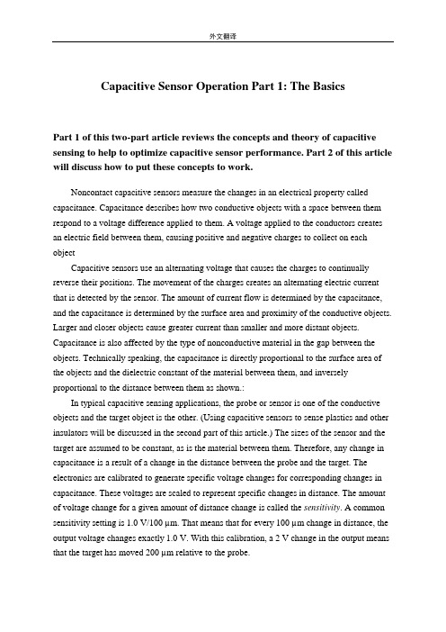
Capacitive Sensor Operation Part 1: The BasicsPart 1 of this two-part article reviews the concepts and theory of capacitive sensing to help to optimize capacitive sensor performance. Part 2 of this article will discuss how to put these concepts to work.Noncontact capacitive sensors measure the changes in an electrical property called capacitance. Capacitance describes how two conductive objects with a space between them respond to a voltage difference applied to them. A voltage applied to the conductors creates an electric field between them, causing positive and negative charges to collect on each objectCapacitive sensors use an alternating voltage that causes the charges to continually reverse their positions. The movement of the charges creates an alternating electric current that is detected by the sensor. The amount of current flow is determined by the capacitance, and the capacitance is determined by the surface area and proximity of the conductive objects. Larger and closer objects cause greater current than smaller and more distant objects. Capacitance is also affected by the type of nonconductive material in the gap between the objects. Technically speaking, the capacitance is directly proportional to the surface area of the objects and the dielectric constant of the material between them, and inversely proportional to the distance between them as shown.:In typical capacitive sensing applications, the probe or sensor is one of the conductive objects and the target object is the other. (Using capacitive sensors to sense plastics and other insulators will be discussed in the second part of this article.) The sizes of the sensor and the target are assumed to be constant, as is the material between them. Therefore, any change in capacitance is a result of a change in the distance between the probe and the target. The electronics are calibrated to generate specific voltage changes for corresponding changes in capacitance. These voltages are scaled to represent specific changes in distance. The amount of voltage change for a given amount of distance change is called the sensitivity. A common sensitivity setting is 1.0 V/100 µm. That means that for every 100 µm change in distance, the output voltage changes exactly 1.0 V. With this calibration, a 2 V change in the output means that the target has moved 200 µm relative to the probe.Focusing the Electric FieldWhen a voltage is applied to a conductor, the electric field emanates from every surface. In a capacitive sensor, the sensing voltage is applied to the sensing area of the probe. For accurate measurements, the electric field from the sensing area needs to be contained within the space between the probe and the target. If the electric field is allowed to spread to other items—or other areas on the target—then a change in the position of the other item will be measured as a change in the position of the target. A technique called "guarding" is used to prevent this from happening. To create a guard, the back and sides of the sensing area are surrounded by another conductor that is kept at the same voltage as the sensing area itself. When the voltage is applied to the sensing area, a separate circuit applies the exact same voltage to the guard. Because there is no difference in voltage between the sensing area and the guard, there is no electric field between them. Any other conductors beside or behind the probe form an electric field with the guard instead of with the sensing area. Only the unguarded front of the sensing area is allowed to form an electric field with the target.DefinitionsSensitivity indicates how much the output voltage changes as a result of a change in the gap between the target and the probe. A common sensitivity is 1 V/0.1 mm. This means that for every 0.1 mm of change in the gap, the output voltage will change 1 V. When the output voltage is plotted against the gap size, the slope of the line is the sensitivity.A system's sensitivity is set during calibration. When sensitivity deviates from the ideal value this is called sensitivity error, gain error, or scaling error. Since sensitivity is the slope of a line, sensitivity error is usually presented as a percentage of slope, a comparison of the ideal slope with the actual slope.Offset error occurs when a constant value is added to the output voltage of the system. Capacitive gauging systems are usually "zeroed" during setup, eliminating any offset deviations from the original calibration. However, should the offset error change after the system is zeroed, error will be introduced into the measurement. Temperature change is the primary factor in offset error.Sensitivity can vary slightly between any two points of data. The accumulated effect of this variation is called linearity erro. The linearity specification is the measurement of how far the output varies from a straight line.To calculate the linearity error, calibration data are compared to the straight line that would best fit the points. This straight reference line is calculated from the calibration data using least squares fitting. The amount of error at the point on the calibration line furthest away from this ideal line is the linearity error. Linearity error is usually expressed in terms ofpercent of full scale (%/F.S.). If the error at the worst point is 0.001 mm and the full scale range of the calibration is 1 mm, the linearity error will be 0.1%.Note that linearity error does not account for errors in sensitivity. It is only a measure of the straightness of the line rather than the slope of the line. A system with gross sensitivity errors can still be very linear.Error band accounts for the combination of linearity and sensitivity errors. It is the measurement of the worst-case absolute error in the calibrated range. The error band is calculated by comparing the output voltages at specific gaps to their expected value. The worst-case error from this comparison is listed as the system's error band. In Figure 7, the worst-case error occurs for a 0.50 mm gap and the error band (in bold) is –0.010.Gap (mm)Expected Value (VDC)Actual Value VDC)Error (mm) 0.50 –10.000 –9.800 –0.0100.75 –5.000 –4.900 –0.0051.00 0.000 0.000 0.0001.25 5.000 5.000 0.0001.50 10.000 10.100 0.005Figure 7. Error valuesBandwidth is defined as the frequency at which the output falls to –3 dB, a frequency that is also called the cutoff frequency. A –3 dB drop in the signal level is an approximately 30% decrease. With a 15 kHz bandwidth, a change of ±1 V at low frequency will only produce a ±0.7 V change at 15 kHz. Wide-bandwidth sensors can sense high-frequency motion and provide fast-responding outputs to maximize the phase margin when used in servo-control feedback systems; however, lower-bandwidth sensors will have reduced output noise which means higher resolution. Some sensors provide selectable bandwidth to maximize either resolution or response time.Resolution is defined as the smallest reliable measurement that a system can make. The resolution of a measurement system must be better than the final accuracy the measurement requires. If you need to know a measurement within 0.02 µm, then the resolution of the measurement system must be better than 0.02 µm.The primary determining factor of resolution is electrical noise. Electrical noise appears in the output voltage causing small instantaneous errors in the output. Even when theprobe/target gap is perfectly constant, the output voltage of the driver has some small butmeasurable amount of noise that would seem to indicate that the gap is changing. This noise is inherent in electronic components and can be minimized, but never eliminated.If a driver has an output noise of 0.002 V with a sensitivity of 10 V/1 mm, then it has an output noise of 0.000,2 mm (0.2 µm). This means that at any instant in time, the output could have an error of 0.2 µm.The amount of noise in the output is directly related to bandwidth. Generally speaking, noise is distributed over a wide range of frequencies. If the higher frequencies are filtered before the output, the result is less noise and better resolution (Figures 8, 9). When examining resolution specifications, it is critical to know at what bandwidth the specifications apply.Capacitive Sensor Operation Part 2: System OptimizationPart 2 of this two-part article focuses on how to optimize the performance of your capacitive sensor, and to understand how target material, shape, and size will affect the sensor's response.Effects of Target SizeThe target size is a primary consideration when selecting a probe for a specific application. When the sensing electric field is focused by guarding, it creates a slightly conical field that is a projection of the sensing area. The minimum target diameter is usually 130% of the diameter of the sensing area. The further the probe is from the target, the larger the minimum target size.Range of MeasurementThe range in which a probe is useful is a function of the size of the sensing area. The greater the area, the larger the range. Because the driver electronics are designed for a certain amount of capacitance at the probe, a smaller probe must be considerably closer to the target to achieve the desired amount of capacitance. In general, the maximum gap at which a probe is useful is approximately 40% of the sensing area diameter. Typical calibrations usually keep the gap to a value considerably less than this. Although the electronics are adjustable during calibration, there is a limit to the range of adjustment.Multiple Channel SensingFrequently, a target is measured simultaneously by multiple probes. Because the system measures a changing electric field, the excitation voltagefor each probe must be synchronized or the probes will interfere with each other. If they were not synchronized, one probe would be trying to increase the electric field while another was trying to decrease it; the result wouldbe a false reading. Driver electronics can be configured as masters or slaves; the master sets the synchronization for the slaves in multichannel systems.Effects of Target MaterialThe sensing electric field is seeking a conductive surface. Provided that the target is a conductor, capacitive sensors are not affected by the specific target material; they will measure all conductors—brass, steel, aluminum, or salt water—as the same. Because the sensing electric field stops at the surface of the conductor, target thickness does not affect the measurement中文翻译电容式传感器操作第一部分:基础 这篇文章的第一部分回顾了电容式传感器的概念和理论来帮助我们优化电容式传感器的性能。
传感器技术0绪论中英对照

Dr. Jinbo Fu
Chapter1:Preface
14
么么么么方面
Sds绝对是假的
Requirements of sensors 传感器的要求
足够的容量(sufficient capacity)—传感器的工作范围或量程(range)足
够大,具有一定的过载能力(overload capacity)。
Wide range of knowledge in Physics, Mechanics, Electronics, Machinery, Optics, etc. 物理、力学、电子学、机械、光学等等 广泛的知识
Good attitude & some devotion 好的学习态度 + 一些投入
Sensor/Transducer Technology
传感器技术
Instructor: Dr. Jinbo Fu (符金波)
Ph.D. of Mechanical Engineering, Penn State Univ., USA M.S. of Electrical Engineering, Penn State Univ., USA M.S. of Mechanical Engineering, Penn State Univ., USA M.E. of Precision Instrument, Tsinghua Univ., PRC B.E. of Precision Instrument, Tsinghua Univ., PRC
状态量 Quantity of
state
颜色color、透明度clarity、磨损量amount of wear、材料内部裂缝或缺陷internal fracture or defect of material、气体泄漏air leak、表面质量
传感器的基础知识中英文对照外文翻译文献

中英文对照外翻译Basic knowledge of transducersA transducer is a device which converts the quantity being measured into an optical, mechanical, or-more commonly-electrical signal. The energy-conversion process that takes place is referred to as transduction.Transducers are classified according to the transduction principle involved and the form of the measured. Thus a resistance transducer for measuring displacement is classified as a resistance displacement transducer. Other classification examples are pressure bellows, force diaphragm, pressure flapper-nozzle, and so on.1、Transducer ElementsAlthough there are exception ,most transducers consist of a sensing element and a conversion or control element. For example, diaphragms,bellows,strain tubes and rings, bourdon tubes, and cantilevers are sensing elements which respond to changes in pressure or force and convert these physical quantities into a displacement. This displacement may then be used to change an electrical parameter such as voltage, resistance, capacitance, or inductance. Such combination of mechanical and electrical elements form electromechanical transducing devices or transducers. Similar combination can be made for other energy input such as thermal. Photo, magnetic and chemical,giving thermoelectric, photoelectric,electromaanetic, and electrochemical transducers respectively.2、Transducer SensitivityThe relationship between the measured and the transducer output signal is usually obtained by calibration tests and is referred to as the transducer sensitivity K1= output-signal increment / measured increment . In practice, the transducer sensitivity is usually known, and, by measuring the output signal, the input quantity is determined from input= output-signal increment / K1.3、Characteristics of an Ideal TransducerThe high transducer should exhibit the following characteristicsa) high fidelity-the transducer output waveform shape be a faithful reproduction of the measured; there should be minimum distortion.b) There should be minimum interference with the quantity being measured; the presence of the transducer should not alter the measured in any way.c) Size. The transducer must be capable of being placed exactly where it is needed.d) There should be a linear relationship between the measured and the transducer signal.e) The transducer should have minimum sensitivity to external effects, pressure transducers,for example,are often subjected to external effects such vibration and temperature.f) The natural frequency of the transducer should be well separated from the frequency and harmonics of the measurand.4、Electrical TransducersElectrical transducers exhibit many of the ideal characteristics. In addition they offer high sensitivity as well as promoting the possible of remote indication or mesdurement. Electrical transducers can be divided into two distinct groups:a) variable-control-parameter types,which include:i)resistanceii) capacitanceiii) inductanceiv) mutual-inductance typesThese transducers all rely on external excitation voltage for their operation.b) self-generating types,which includei) electromagneticii)thermoelectriciii)photoemissiveiv)piezo-electric typesThese all themselves produce an output voltage in response to the measurand input and their effects are reversible. For example, a piezo-electric transducer normally produces an output voltage in response to the deformation of a crystalline material; however, if an alternating voltage is applied across the material, the transducer exhibits the reversible effect by deforming or vibrating at the frequency of the alternating voltage.5、Resistance TransducersResistance transducers may be divided into two groups, as follows:i) Those which experience a large resistance change, measured by using potential-divider methods. Potentiometers are in this group.ii)Those which experience a small resistance change, measured by bridge-circuit methods. Examples of this group include strain gauges and resistance thermometers.5.1 PotentiometersA linear wire-wound potentiometer consists of a number of turns resistance wire wound around a non-conducting former, together with a wiping contact which travels over the barwires. The construction principles are shown in figure which indicate that the wiperdisplacement can be rotary, translational, or a combination of both to give a helical-type motion. The excitation voltage may be either a.c. or d.c. and the output voltage is proportional to the input motion, provided the measuring device has a resistance which is much greater than the potentiometer resistance.Such potentiometers suffer from the linked problem of resolution and electrical noise. Resolution is defined as the smallest detectable change in input and is dependent on thecross-sectional area of the windings and the area of the sliding contact. The output voltage is thus a serials of steps as the contact moves from one wire to next.Electrical noise may be generated by variation in contact resistance, by mechanical wear due to contact friction, and by contact vibration transmitted from the sensing element. In addition, the motion being measured may experience significant mechanical loading by the inertia and friction of the moving parts of the potentiometer. The wear on the contacting surface limits the life of a potentiometer to a finite number of full strokes or rotations usually referred to in the manufacture’s specification as the ‘number of cycles of life expectancy’, a typical value being 20*1000000 cycles.The output voltage V0 of the unload potentiometer circuit is determined as follows. Let resistance R1= xi/xt *Rt where xi = input displacement, xt= maximum possible displacement, Rt total resistance of the potentiometer. Then output voltage V0= V*R1/(R1+( Rt-R1))=V*R1/Rt=V*xi/xt*Rt/Rt=V*xi/xt. This shows that there is a straight-line relationship between output voltage and input displacement for the unloaded potentiometer.It would seen that high sensitivity could be achieved simply by increasing the excitation voltage V. however, the maximum value of V is determined by the maximum power dissipation P of the fine wires of the potentiometer winding and is given by V=(PRt)1/2 .5.2 Resistance Strain GaugesResistance strain gauges are transducers which exhibit a change in electrical resistance in response to mechanical strain. They may be of the bonded or unbonded variety .a) bonded strain gaugesUsing an adhesive, these gauges are bonded, or cemented, directly on to the surface of the body or structure which is being examined.Examples of bonded gauges arei) fine wire gauges cemented to paper backingii) photo-etched grids of conducting foil on an epoxy-resin backingiii)a single semiconductor filament mounted on an epoxy-resin backing with copper or nickel leads.Resistance gauges can be made up as single elements to measuring strain in one direction only,or a combination of elements such as rosettes will permit simultaneous measurements in more than one direction.b) unbonded strain gaugesA typical unbonded-strain-gauge arrangement shows fine resistance wires stretched around supports in such a way that the deflection of the cantilever spring system changes the tension in the wires and thus alters the resistance of wire. Such an arrangement may be found in commercially available force, load, or pressure transducers.5.3 Resistance Temperature TransducersThe materials for these can be divided into two main groups:a) metals such as platinum, copper, tungsten, and nickel which exhibit and increase in resistance as the temperature rises; they have a positive temperature coefficient of resistance.b) semiconductors, such as thermistors which use oxides of manganese, cobalt, chromium, or nickel. These exhibit large non-linear resistance changes with temperature variation and normally have a negative temperature coefficient of resistance.a) metal resistance temperature transducersThese depend, for many practical purpose and within a narrow temperature range, upon the relationship R1=R0*[1+a*(b1-b2)] where a coefficient of resistance in ℃-1,and R0 resistance in ohms at the reference temperature b0=0℃ at the reference temperature range ℃.The international practical temperature scale is based on the platinum resistance thermometer, which covers the temperature range -259.35℃ to 630.5℃.b) thermistor resistance temperature transducersThermistors are temperature-sensitive resistors which exhibit large non-liner resistance changes with temperature variation. In general, they have a negative temperature coefficient. For small temperature increments the variation in resistance is reasonably linear; but, if large temperature changes are experienced, special linearizing techniques are used in the measuring circuits to produce a linear relationship of resistance against temperature.Thermistors are normally made in the form of semiconductor discs enclosed in glass vitreous enamel. Since they can be made as small as 1mm,quite rapid response times are possible.5.4 Photoconductive CellsThe photoconductive cell , uses a light-sensitive semiconductor material. The resistance between the metal electrodes decrease as the intensity of the light striking the semiconductor increases. Common semiconductor materials used for photo-conductive cells are cadmium sulphide, lead sulphide, and copper-doped germanium.The useful range of frequencies is determined by material used. Cadmium sulphide is mainly suitable for visible light, whereas lead sulphide has its peak response in the infra-red regionand is, therefore , most suitable for flame-failure detection and temperature measurement. 5.5 Photoemissive CellsWhen light strikes the cathode of the photoemissive cell are given sufficient energy to arrive the cathode. The positive anode attracts these electrons, producing a current which flows through resistor R and resulting in an output voltage V.Photoelectrically generated voltage V=Ip.RlWhere Ip=photoelectric current(A),and photoelectric current Ip=Kt.BWhere Kt=sensitivity (A/im),and B=illumination input (lumen)Although the output voltage does give a good indication of the magnitude of illumination, the cells are more often used for counting or control purpose, where the light striking the cathode can be interrupted.6、Capacitive TransducersThe capacitance can thus made to vary by changing either the relative permittivity, the effective area, or the distance separating the plates. The characteristic curves indicate that variations of area and relative permittivity give a linear relationship only over a small range of spacings. Thus the sensitivity is high for small values of d. Unlike the potentionmeter, the variable-distance capacitive transducer has an infinite resolution making it most suitable for measuring small increments of displacement or quantities which may be changed to produce a displacement.7、Inductive TransducersThe inductance can thus be made to vary by changing the reluctance of the inductive circuit. Measuring techniques used with capacitive and inductive transducers:a)A.C. excited bridges using differential capacitors inductors.b)A.C. potentiometer circuits for dynamic measurements.c) D.C. circuits to give a voltage proportional to velocity for a capacitor.d) Frequency-modulation methods, where the change of C or L varies the frequency of an oscillation circuit.Important features of capacitive and inductive transducers are as follows:i)resolution infiniteii) accuracy+- 0.1% of full scale is quotediii)displacement ranges 25*10-6 m to 10-3miv) rise time less than 50us possibleTypical measurands are displacement, pressure, vibration, sound, and liquid level.8、Linear Variable-differential Ttransformer9、Piezo-electric Transducers10、Electromagnetic Transducers11、Thermoelectric Transducers12、Photoelectric Cells13、Mechanical Transducers and Sensing Elements传感器的基础知识传感器是一种把被测量转换为光的、机械的或者更平常的电信号的装置。
电容式传感器的外文文献翻译、中英文翻译、外文翻译
参考资料原文:Capacitive sensors and the main features of the basic concepts: The measured volume of the machinery, such as displacement, pressure change is converted to the sensor capacitance. It is the sensitive part of the capacitor with variable parameters. Its most common form is composed of two parallel electrodes, a very inter-air as the medium of the capacitor, if the neglect edge effects, the capacitance for the capacitor plate ε A / δ, where εis a very inter-medium dielectric constant, A two electrode effective area covered by each other, δ is the distance between two electrodes. δ, A, εone of the three parameters will lead to the change in capacitance changes can be used for measurement. Therefore capacitive sensors can be divided into polar distance change type, change type size, media type three types of changes.Most from the changes in small type generally used to measure the linear displacement, or as a result of force, pressure, vibration caused by changes in polar distance (see capacitive pressure sensors). Change type size generally used to measure the angular displacement or linear displacement larger. Changes in media type commonly used in level measurement and a variety of media, temperature, density, humidity measurement. The advantage of the sensor capacitor structure is simple, inexpensive, high sensitivity,过载能力strong, good dynamic response and high temperature, radiation, vibration and other adverse conditions of strong adaptability and strong. The disadvantage is that there are non-linear output, parasitic capacitance and the distributed capacitance on the sensitivity and accuracy the impact of larger and more complex circuits, such as connectivity. Since the late 70s, with the development of integrated circuit technology, a packaging and micro-measuring instrument with capacitive sensors.This new type of distributed capacitance sensors can greatly reduce the impact to overcome the inherent drawbacks. Capacitive sensor is a very wide use, a great potential for development of the sensor.Capacitive sensor working principle:Capacitive sensor surface of the induction of two coaxial metal electrode composition, much like "open" capacitor electrode, the two electrodes form a capacitor, in series with the RC oscillation circuit. Power when connected, RC oscillator is notoscillating, when a goal of moving around electrical capacitor, the capacitor capacity increased, the oscillator to start oscillation. Circuit after the passage of the deal, will be two kinds of vibration and vibration signals into switching signals, which played a detection purpose of the existence of any objects. The sensor can detect metal objects, but also to detect non-metallic objects, metal objects can move away from the largest, non-metallic objects on the decision to move away from the dielectric constant material, the greater the dielectric constant materials, the availability of action the greater distance.Application of capacitive sensors:Capacitive sensor can be used to measure linear displacement, angular displacement, vibration amplitude, especially suitable for measuring high-frequency vibration amplitude, precision rotary axis accuracy, acceleration and other mechanical parameters. Pole-changing type of application from a smaller displacement in the measurement range to several hundred microns in 0.01m, precision can reach 0.01m, a resolution of up to 0.001m. Change type size larger displacement can be measured, for the zero-range a few millimeters to a few hundred mm, 0.5 percent better than the linear resolution of 0.01 ~ 0.001m. Capacitive angular displacement sensor point of view and the dynamic range to a few degrees, a resolution of about 0.1 "up to the stability of the zero angle-second, widely used in precision angle measurement, such as for high-precision gyroscopes and accelerometers tilting . capacitive measurement sensor can measure the peak amplitude for the 0 ~ 50m, a frequency of 10 ~ 2kHz, sensitivity is higher than 0.01m, non-linear error of less than 0.05m.Capacitive sensor can also be used to measure pressure, differential pressure, level, surface, composition content (such as oil, the water content of food), non-metallic coating materials, such as film thickness, dielectric measurements of humidity, density, thickness, etc., in the automatic detection and control systems are also often used as a location signal generator. Capacitive differential pressure sensor measuring range up to 50MPa, an accuracy of ± 0.25% ~ ± 0.5%. Capacitive sensor for measuring range of the thickness of a few hundred microns, resolution of up to 0.01m. Capacitive Proximity Switches can not only detect metal, but also can detect plastic, wood,paper, and other dielectric liquids, but can not achieve the ultra-small, the movement distance of about 10 ~ 20mm. Electrostatic capacitive level switch is widely used in detection is stored in the tank, hopper, such as the location of containers in a variety of objects of a mature product. When the capacitive sensor measuring metal surface conditions, from the size, vibration amplitude is often used very variable from unilateral type, when the measured object is a capacitor electrode, and the other electrode in the sensor inside. This type of sensor is a non-contact measurement, dynamic range is relatively small, about a few millimeters is about the precision of more than 0.1m, a resolution of 0.01 ~ 0.001m.译文:电容式传感器的基本概念及主要特点:把被测的机械量,如位移、压力等转换为电容量变化的传感器。
传感器中英文介绍
. sensorssensors(English name: transducer/sensor) is a kind of detection device, can feel the measured information, and will feel information transformation according to certain rule become electrical signal output, or other form of information needed to satisfy the information transmission, processing, storage, display, record and control requirements.Sensor's features include: miniaturization, digital, intelligent, multi-functional, systematic and network. It is the first step of automatic detection and automatic control. The existence and development of the sensor, let objects have sensory, such as touch, taste and smell let objects become live up slowly. Usually according to its basic cognitive functions are divided into temperature sensor, light sensor, gas sensor, force sensor, magnetic sensor, moisture sensor, acoustic sensor, radiation sensitive element, color sensor and sensor etc. 10 major categories.temperature transducerTemperature sensors (temperature transducer) refers to can feel temperature translates into usable output signal of the sensor. The temperature sensor is the core part of the temperature measuring instrument, wide variety. According to measuring methods could be divided into two types: contact and non-contact, according to the sensor material and electronic component features divided into two categories, thermal resistance and thermocouple.1 principle of thermocoupleThermocouple is composed of two different materials of metal wire, the welded together at the end. To measure the heating part of the environment temperature, can accurately know the temperature of the hot spots. Because it must have two different material of the conductor, so called the thermocouple. Different material to make the thermocouple used in different temperature range, their sensitivity is also each are not identical. The sensitivity of thermocouple refers to add 1 ℃hot spot temperature changes, the output variation of potential difference. For most of the metal material support thermocouple, this value about between 5 ~ 40 microvolt / ℃.As a result of the thermocouple temperature sensor sensitivity has nothing to do with the thickness of material, use very fine material also can make the temperature sensor. Also due to the production of thermocouple metal materials have good ductility, the slight temperature measuring element has high response speed, can measure the process of rapid change.Its advantages are:(1)high precision measurement. Because of thermocouple direct contact with the object being measured, not affected by intermediate medium.(2)the measurement range. Commonly used thermocouple from 1600 ℃to 50 ℃ ~ + sustainable measurement, some special thermocouple minimum measurable to - 269 ℃ (e.g., gold iron nickel chrome), the highest measurable to + 2800 ℃ (such as tungsten rhenium).(3) simple structure, easy to use. Thermocouple is usually composed of two different kinds of metal wire, but is not limited by the size and the beginning of, outside has protective casing, so very convenient to use. The thermocouple type and structure of the form.2. The thermocouple type and structure formation(1)the types of thermocoupleThe commonly used thermocouple could be divided into two types: standard thermocouple and non-standard thermocouple. Standard thermocouple refers to the national standard specifies its thermoelectric potential and the relationship between temperature, permissible error, and a unified standard score table of thermocouple, it has with matching display instrument to choose from. Rather than a standard thermocouple or on the order of magnitude less than the range to use standardized thermocouple, in general, there is no uniform standard, it is mainly used for measurement of some special occasions.Standardized thermocouple is our country from January 1, 1988, thermocouple and thermal resistance of all production according to IEC international standard, and specify the S, B, E, K, R, J, T seven standardization thermocouple type thermocouple for our country unified design.(2)to ensure that the thermocouple is reliable, steady work, the structure of thermocouple requirements are as follows:①of the two thermocouple thermal electrode welding must be strong;②two hot electrode should be well insulated between each other, in case of short circuit;③compensation wires connected to the free cod of a thermocouple to convenient and reliable;④protect casing thermal electrodes should be able to make sufficient isolation and harmful medium.3.The thermocouple cold end temperature compensationDue to the thermocouple materials are generally more expensive (especiallywhen using precious metals), and the temperature measurement points are generally more far, the distance to the instrument in order to save materials, reduce cost, usually adopt the compensating conductor) (the free end of the cold junction of the thermocouple to the steady control of indoor temperature, connected to the meter terminals. It must be pointed out that the role of the thermocouple compensation wire extension hot electrode, so that only moved to the control room of the cold junction of the thermocouple instrument on the terminal, it itself does not eliminate the cold end temperature change on the influence of temperature, cannot have the compensation effect. So, still need to take some of the other correction method to compensate of the cold end temperature especially when t0 indicates influence on measuring temperature 0 ℃.Must pay attention to when using thermocouple compensating conductor model match, cannot be wrong polarity, compensation conductor should be connected to the thermocouple temperature should not exceed 100 ℃.传感器传感器(英文名称:transducer/sensor)是一种检测装置,能感受到被测量的信息,并能将感受到的信息,按一定规律变换成为电信号或其他所需形式的信息输出,以满足信息的传输、处理、存储、显示、记录和控制等要求。
- 1、下载文档前请自行甄别文档内容的完整性,平台不提供额外的编辑、内容补充、找答案等附加服务。
- 2、"仅部分预览"的文档,不可在线预览部分如存在完整性等问题,可反馈申请退款(可完整预览的文档不适用该条件!)。
- 3、如文档侵犯您的权益,请联系客服反馈,我们会尽快为您处理(人工客服工作时间:9:00-18:30)。
4.1 工作原理、结构及特性
2
ef
0 0
/ 0 100% 0 100%
0
0
(4-9)
由上讨论可知:
(1)变极距型电容传感器只有在|Δδ0/δ0| 很小(小测量范围) 时,才有近似的线性输出;
(2)灵敏度S与初始极距δ0的平方成反比,故可用减少δ0的办 法来提高灵敏度。例如在电容式压力传感器中,常取δ0= 0.1~0.2mm,C0在20~100pF之间。由于变极距型的分辨力 极高,可测小至0.01μm的线位移,故在微位移(micro displacement)检测中应用最广。
4.1 工作原理、结构及特性
4.1.1 变极距型电容传感器
图4-1为这种传感器的原理图。当传感器的εr和A为常数,初 始极距为δ0 ,由式(4-1)可知其初始电容量C0为
C0 0r A / 0 (4-2)
图4.1 变极距型电容传感器原理图
4.1 工作原理、结构及特性
如果满足条件(Δδ0/δ0)<<1,式(4-4)可按级数展开(series expansion)成CLeabharlann /C00 0
1
0 0
0 0
2
0 0
3
(4-5)
4.1 工作原理、结构及特性
略去高次(非线性)项,可得近似的线性关系和灵敏度S
分别为
C
/ C0
0 0
距离δ有关:C=ε0εrA/δ (4-1)
➢ 若被测量的变化使式中δ、A、εr三个参量中任意一个发生变 化时,都会引起电容量的变化,再通过测量电路就可转换为 电量输出。因此,电容式传感器可分为变极距型(variable electrode distance)、变面积型(variable area)和变介质型 (variable medium)三种类型 。
第4章 电容式传感器
Capacitance Type Sensors
第4章 电容式传感器
4.1 工作原理、结构和特性
Principle, structure and characteristics
41.2 应用中存在的问题及其改进措施
Existing problems and improvements
4.1 工作原理、结构及特性
由式(4-9)可见, δ0的减小会导致非线性误差增大;δ0过小 还可能引起电容器击穿(break down)或短路(short circuit)。 为此,极板间可采用高介电常数(permittivity)的材料(云母 (Mica)、塑料膜(plastic film)等)作介质,如图4.4所示。设 两种介质的相对介电质常数为εr1 (空气:εr1=1)、εr2, 相应的介质厚度为δ1、δ2,则有
(4-6)
和
S
C
/
0
C0
/0
0 r
A
/
2 0
(4-7)
如果考虑式(4-5)中的线性项(linear term)及二次项 (quadratic term),则
C
/
C0
0 0
1
0 0
(4-8)
4.1 工作原理、结构及特性
式(4-6)的特性如图4.3中的直线1,而式(4-8)的特性如 曲线2。因此,以式4-6作为传感器的特性使用时,其相 对非线性误差(error of nonlinearity) ef为
变化量为
C
/ C0
C1 C2 C0
2
0
1
0
2
0
4
(4-11)
4.1 工作原理、结构及特性
略去高次项(higher order terms),可得近似的线性关系
一种很有发展前途的传感器。
4.1 工作原理、结构及特性
第一节 工作原理、结构和特性
➢ 由绝缘介质(insulation medium)分开的两个平行金属板组成的 平板电容器(plate capacitor),当忽略边缘效应(edge effect)影 响时,其电容量(capacitance)与真空介电常数(permittivity of vacuum)ε0 (8.854×10⁻¹²F/m)、极板间介质的相对介电常 数(relative permittivity)εr、极板的有效面积A以及两极板间的
4.1 工作原理、结构及特性
C
0 A
1 2 / r 2
(4-10)
图4.5所示为差动结构(differential structure),动极板置于两定 极板(fixed electrode plate)之间。初始位置(initial position)时, δ1=δ2=δ0,两边初始电容(initial capacitance)相等。当动 极板(movable plate)向上有位移Δδ时,两边极距为δ1=δ0Δδ,δ2 =δ0+Δδ; 两组电容一增一减。同差动式自感传 感器的同样分析方法,由式(4-4)和式(4-5)可得电容总的相对
当动极端板因被测量变化而向上移动使δ0减小Δδ0时,电容量 增大ΔC则有
C0 C 0r A/ 0 0 C0 / 1 0 /0 (4-3)
可见,传感器输出特性C=f(δ)是非线性的,如图4-2所示。电
容相对变化量为
1
C / C0
0 0
1
0 0
(4-4)
4.3 测量电路
Measurement circuits
4.4 电容式传感器及其应用
Capacitance sensors and applications
第4章 电容式传感器
➢ 电容式传感器(capacitance type sensors)是将 被测非电量的变化转换为电容量变化的一种传 感器。结构简单、分辨力高(high resolution)、 可非接触测量(contactless measurement),并 能在高温、辐射(radiation)和强烈振动(strong vibration)等恶劣条件下工作,这是它的独特优 点。随着集成电路(IC-Integrated Circuit)技术 和计算机技术的发展,促使它扬长避短,成为