ARM仿真器用户手册
J-Link 仿真器 说明书 (本手册适 V6.0、V7.0、V8.0 版本的 J-LINK)

J-Link用户指南(本手册适用于V6.0、V7.0、V8.0版本的J-LINK)1.J-Link ARM JTAG 仿真器简介J-Link 是 SEGGER 公司为支持仿真 ARM 内核芯片推出的 JTAG仿真器。
配合 IAR EWARM,ADS,KEIL,WINARM,RealView 等集成开发环境支持所有 ARM7/ARM9 内核芯片的仿真,通过 RDI 接口和各集成开发环境无缝连接,操作方便、连接方便、简单易学,是学习开发 ARM 最好最实用的开发工具。
J-Link ARM 主要特点* IAR EWARM 集成开发环境无缝连接的JTAG 仿真器* 支持所有 ARM7/ARM9 内核的芯片,以及 cortex M3,包括 Thumb 模式* 支持 ADS,IAR,KEIL,WINARM,REALVIEW 等几乎所有的开发环境* 下载速度高达 ARM7:600kB/s,ARM9:550kB/s,通过 DCC 最高可达 800 kB/s* 最高 JTAG 速度 12 MHz* 目标板电压范围 1.2V –3.3V,兼容5V* 自动速度识别功能* 监测所有 JTAG 信号和目标板电压* 完全即插即用* 使用 USB 电源(但不对目标板供电)* 带 USB 连接线和 20 芯扁平电缆* 支持多 JTAG 器件串行连接* 标准 20 芯JTAG 仿真插头* 选配 14 芯 JTAG 仿真插头* 带J-Link TCP/IP server,允许通过 TCP/ IP 网络使用J-LinkJ-Link 支持 ARM 内核* ARM7TDMI(Rev 1)* ARM7TDMI(Rev 3)* ARM7TDMI-S(Rev 4)* ARM720T * ARM920T*ARM926EJ-S*ARM946E-S*ARM966E-S* ARM11* Cortex-M3速度信息RevisionARM7Memory downloadARM9Memory downloadJ-Link Rev. 1-4 150.0 kB/s(4MHz JTAG)75.0 kB/s(4MHz JTAG)J-Link Rev. 5-8720.0 kB/s(12MHz JTAG)550.0 kB/s(12MHz JTAG)J-Trace Rev. 1420.0 kB/s(12MHz JTAG)280.0 kB/s(12MHz JTAG2.J-LINK 驱动安装J-LINK 是本站开发的兼容产品,具有一样的性能,但是却只有十分之一的价格!首先到/download_jlink.html 下载最新的 J-LINK驱动软,J-Link ARM software and documentation pack ,内含USB driver, J-Mem, J-Link.exe and DLL for ARM, J-Flash and J-Link RDI。
ARM_JTAG实时仿真器安装使用指南131新

ARM JTAG实时仿真器安装使用指南Version 1.312003. 11. 12目录第一章 ARM JTAG介绍JTAG产品介绍 (3)ARM第二章 ARM开发系统安装硬件连接 (4)2.1软件安装 (4)2.2第三章 ARM JTAG简单使用3.1 硬件连接 (18)软件使用 (18)3.23.2.1 启动Multi-ICE Server (18)3.2.2 启动ADS (21)第四章 ARM JTAG使用详解Multi-ICEServer使用 (33)4.1Server菜单选项..... (33)Multi-ICE4.1.1Server状态 (34)4.1.2Multi-ICEServer中的JTAG参数设置.......... . (38)Multi-ICE4.1.34.1.4 Multi-ICE Server配置 .................... . (40)调试系统架构体系 (41)4.24.3 ADS V1.2与ARM JTAG连接 (42)4.3.1 连接AXD (42)4.3.2 连接CodeWarrior (43)第五章最终应用程序烧写5.1应用程序在ARM板上运行原理 (45)生成“Boot.bin ” (45)5.25.2.1系统初始化 (45)5.2.2生成BIN文件 (45)烧录“Boot.bin” (47)5.3第六章ARM JTAG硬件介绍JTAG接口定义 (48)6.1ARMARMJTAG接口电平 (49)6.2TCK信号频率设置 (49)6.3RTCK时钟 (49)6.514脚和20脚JTAG接口转换 (50)6.6附录1 TCK频率设置 (51)附录2 常见问题 (53)2第一章 ARM JTAG介绍ARM JTAG产品介绍JTAG是用于ARM处理器内核软件调试的专用工具,符合IEEE 1149.1规范,与ARM原装 ARMMulti-ICE完全兼容。
ARM开发板使用手册

ARM开发板使用手册PHILIP LPC2132ARM7TDMI第一章介绍LPC2132开发板是专门为arm 初学者开发的实验板,用户可以做基础的arm实验,也可以做基于ucos-ii的操作系统实验。
本系统的实验源代码全部开放,用户可以在此基础上开发产品,减少重复劳动。
由于LPC2132体积很小,并且功能强大,因此特别适合需要复杂智能控制的场合,其运行速度高于早期的80486计算机,而体积只有指甲大。
我们已经将LPC2132产品成功应用在干扰比较强的工业场合,经过6个月的运行,各项指标符合要求。
因此我们特别推荐这一款开发板作为ARM初学者入门。
由于此款开发板体积很小,非常适合直接应用在工业以及民用智能控制器的场合。
LPC2132 CPU介绍LPC2131/2132/2138 是基于一个支持实时仿真和跟踪的16/32 位ARM7TDMI-STM CPU,并带有32kB、64kB 和512kB 嵌入的高速Flash 存储器。
128 位宽度的存储器接口和独特的加速结构使32 位代码能够在最大时钟速率下运行。
对代码规模有严格控制的应用可使用16 位Thumb 模式将代码规模降低超过30%,而性能的损失却很小。
较小的封装和很低的功耗使LPC2131/2132/2138 特别适用于访问控制和POS 机等小型应用中;由于内置了宽范围的串行通信接口和8/16/32kB 的片内SRAM,它们也非常适合于通信网关、协议转换器、软件modem、语音识别、低端成像,为这些应用提供大规模的缓冲区和强大的处理功能。
多个32 位定时器、1个或2 个10 位8 路的ADC、10 位DAC、PWM 通道、47 个GPIO 以及多达9 个边沿或电平触发的外部中断使它们特别适用于工业控制应用以及医疗系统。
主要特性●●16/32 位ARM7TDMI-S 核,超小LQFP64 封装。
●●8/16/32kB 的片内静态RAM 和32/64/512kB 的片内Flash 程序存储器。
Proteus仿真ARM7实验手册
5
选择模板
File > New Design
Proteus 仿真 ARM7 实验手册
选择 Landscape A4 模板 > OK。
选择模板
保存(Save Design):counter
添加模板
中国科学院西安网络中心 © 2007 - ARM7 实验手册
选取元件
Library > Pick Devices/Symbol….。
Edit Component 对话框
单击 Program File 的浏览按钮 ,添加已经编译好的目标程序文件 counter.hex,OK。
中国科学院西安网络中心 © 2007 - 2008
12
单击启动仿真按钮
Proteus 仿真 ARM7 实验手册
,运行仿真,单击电路图中按键可观察到数码管数字增大或减小。
电路原理图
打开 Keil 项目
打开已有的项目:Project > Open Project…
ARM仿真器应用指导
ARM仿真器应用指导ARM仿真器应用指导本文提供了一些关于在线ARM 仿真器的信息,以及给作为嵌入式系统设计师的你带来的好处。
根据你的需要,你将在产品开发中对开发工具作出更恰当的选择。
一、嵌入式产品的开发周期典型的嵌入式微控制器开发项目的第一个阶段是用C编译器从源程序生成目标代码,生成的目标代码将包括物理地址和一些调试信息。
目前代码可以用软件模拟器、目标Monitor或在线仿真器来执行和调试。
软件模拟器是在PC机或工作站平台上,以其CPU(如x86)及其系统资源来模拟目标CPU(如P51XA),并执行用户的目标代码;而目标Monitor则是将生成的目标代码下载到用户目标板的程序存储器中,并在下载的代码中增加一个Monitor任务软件,用来监视和控制用户目标代码的执行,用户通过目标板上的串行口或其它调试端口,利用桌面计算机来调试程序。
程序的调试是通过设置断点、使程序在指定的指令位置停止运行来实现的。
在程序中止的时候,检查存储器和寄存器的内容,作为发现程序错误的线索。
程序经过调试、找到所有的错误后,修改源代码,重新编译,以一种标准格式生成目标代码文件,比如Intel HEX。
这个目标代码将被存储在最终产品的非挥发存储器,比如EPROM或FLASH中。
二、为什么需要仿真器软件模拟器和目标Monitor提供了一种经济的调试手段,对于很多设计来说已经足够。
但是也有很多场合,需要利用仿真器来找到程序错误。
无论在哪一种场合,仿真器都能够减少调试时间、简化系统集成、增加可靠性、优化测试步骤,从而使其物有所值。
更常见的情况是工程师在项目的不同阶段同时使用软件模拟器和仿真器,特别是在大的开发项目中。
软件模拟器和软件调试器在断点之外只提供了很少的几种功能,比如显示端口内容和代码覆盖。
没有检测事件和条件、然后作出反应的手段,也没有办法记录MCU的总线周期、然后判断程序的执行究竟发生了什么情况。
如果你的MCU有片上EPROM或FLASH存储器,并且运行在单片模式,则只有仿真器才能够对系统进行调试,而不严重占用和消耗MCU资源。
ARM HSSTP II Active Probe 用户手册说明书
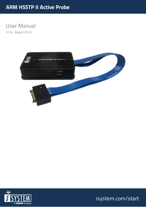
User ManualV2.6, August 2023/startGeneral safety instructionsPlease read the following safety precautions carefully before putting this device to use to avoid any personal injuries, damage to the instrument, or to the target system. Use this instrument only for its intended purpose as specified by this manual to prevent potential hazards.Use included power cord and power supplyThe enclosed power supply has been approved for use by iSYSTEM. Please contact iSYSTEM if you need to consider an alternative power.Use grounding wirePrior to applying power to either the BlueBox or the target, connect the device and the target system together with the included grounding wire. This is to avoid potential damage caused by any voltage difference between the device and the target system.Use proper overvoltage protectionEnsure proper protection to avoid exposing the BlueBox device or the operator to overvoltage surges (e.g. caused by thunderstorm, mains power).Do not operate without coverDo not operate the device with cover removed.Avoid circuit and wire exposureDo not touch exposed components or wires when the device is powered.Do not operate with suspected damageIf you suspect damage may have occurred, the BlueBox device must be inspected by qualified service personnel before further operation.Do not operate the device outside its rated supply voltage or environmental rangeConsult with iSYSTEM before using equipment outside of the parameters provided in this manual.This symbol is used within the manual to highlight further safety notices.ContentsPackage content (4)Specifications (5)Operation (6)mDIO Cable (8)40-pin Samtec ERF8 to 20-pin 2.54mm ARM Converter (9)40-pin Samtec ERF8 to 10-pin 1.27mm CoreSight and 40-pin Samtec ERF8 HSSTP Converter (10)10-pin 1.27mm CoreSight to 20-pin 2.54mm ARM Converter (13)40-pin Samtec / USB-C to USB-C (HSSTP) Switch (14)Hardware Setup and Configuration (18)Accessories (19)Active Probe ARM HSSTP II allows debugging, tracing and testing ARM® Cortex™ architectures. It supports both the JTAG debug interface and ARM High-Speed Trace Port (HSSTP). Its small and compact hardware size allows for connecting to a target microcontroller in a confined space as far as 10 m away. The Active Probe supports up to 4 parallel HSSTP lanes, running at a maximum bitrate of 5Gbps.The ARM HSSTP II Active Probe kit is delivered with the following components:ARM HSSTP II Active Probe 1m FNet CableSamtec40 -to 20-pin JTAGARM AdapterOrdering code: IC57125-1Ordering code:BB-FNET-100Ordering code:IASAM40ARMPIN20Blue colored signals are trace signals.Signal direction definition:O - Output from the Active Probe to the target microcontrollerI - Input to the Active Probe from the target microcontrollerThe target microcontroller connector is a Samtec ERF8 series, rugged high-speed socket, part number ASP-130367-01.B – mDIO port marked as TRIG on the housingmDIO port provides two digital signals, which can interact with the embedded target. Each can be configured either for input or output operation.mDIO port on the Active ProbeC – The indicator light provides the status of the Active Probe as follows:Permanently green – Powered on and ready to use.Blinking green – Establishing connection with the BlueBox.Blinking blue – Reprogramming SPLASH.Permanently magenta – Golden image loaded and ready to use.D – FNet connector, that connects the Active Probe to the iC5700 BlueBox. The FNet cable is delivered with the Active Probe.When powering on the system, switch the iC5700 on before powering on the target. When powering down the system, power off the target before powering off the iC5700!UseConsult with iSYSTEM before attempting to use any other accessory.Ordering code BB-AP-MDIO-20mDIO Cable is used to connect the Active Probe mDIO port with the signals around the debugged microcontroller, which can then be either read or controlled by the debugger. For example, the debugger can periodically service an external watchdog through the mDIO output or just read and record an external signal through the mDIO input. It must be ordered separately. Length of the cable is 20 cm.Ordering code IASAM40ARMPIN20In conjunction with this 40-pin Samtec ERF8 to 20-pin 2.54 ARM converter delivered in the package, the Active Probe can be connected to the target board featuring a 20-pin 2.54 mm ARM target debug connector providing the JTAG debug interface.This converter is required only when the Active Probe is to be connected to the embedded targetdebug interface without the ARM HSSTP tracethe Active Probe.Signal Direction is described from the BlueBox perspective.Ordering code IASAM40HSSTP-JTAGSAM Normally 40-pin ERF8 ARM HSSTP connector provides both, ARM HHSTP trace interface and JTAG or SWD debug interface. However, some targets for some reason don’t connect debug interface to this connector and provide the debug JTAG/SWD interface on a separate debug connector (10-pin 1.27mm CoreSight). Using this adapter, the Active Probe can be properly connected to such target.This converter is required only when the Active Probe is to be connected to the embedded targetJTAG/SWD interface physically connected but has10-pin 1.27 mm CoreSight target debug connector.The adapter doesn’t come along the Active Probe and has to be ordered separately.The converter has the following pinouts:A – 40-pin Samtec ERF8 connector providing merged JTAG/SWD debug signals (C on the image) and the HSSTP trace signals (B on the image) signals, to which the Active ProbeB – 40-pin Samtec ERF8 connector which connects to target development board with 40-pinBlue colored signals are trace signals.C – 10-pin CoreSight connector which connects to the target development board exposingSignal Direction is described from the BlueBox perspective.Related to the just described converter IASAM40HSSTP-JTAGSAM, the target development board can also feature a 20-pin 2.54 mm ARM target debug connector instead of the 10-pin 1.27 mm CoreSight. In order to connect the C part of the IASAM40HSSTP-JTAGSAM to this connector, another converter IA10PINCS20PINARM-1 is required, converting from ARM 20-pin 2.54mm to 10-pin 1.27 CoreSight. The IA10PINCS20PINARM-1 connects to the target and then the ‘C’ point of the IASAM40HSSTP-JTAGSAM connects on top of it.Ordering code IA10PINCS20PINARM-1This converter is required only when the Active Probe is to be connected to the embedded target providing the 20-pin 2.54 mm ARM target debug connector exposing only the debug interface without the ARM HSSTP trace interface. No trace interface (e.g. SWO, parallel) is supported with this converter. The converter is delivered along the Active Probe. Refer to ARM HSSTP II Active Probe User Manual for more information.* nTRST is permanently pulled upSignal Direction is described from the BlueBox perspective.Ordering code IEA-SWITCH-SAM40USBCThrough this hardware switch, you can conveniently connect·ARM HSSTP II Active Probe·and a host PC via a standard USB-C connectionto NVIDIA Orin device (connection marked as ORIN USB-C) at the same time. This switch is optional and must be ordered separately.A use case is that an application is programmed by the PC-based flash programming utility through the USB-C connection, and later, the application is debugged using the ARM HSSTP II Active Probe. Refer to the Technical Note NVIDIA Orin: USB port functionality switching for a use case where the switching can be automated.Switch configurationConnectorsThe switch features two USB-C connectors:·ORIN USB-C with a custom pinout for connection with the NVIDIA Orin device,·HOST USB-C for connection with the host PC (standard USB connection).Blue colored signals are trace signals.* Pulled down with 5k1 resistor.Blue colored signals are trace signals.Signal Direction is described from the BlueBox perspective.When connecting the BlueBox to a target for the first time, doubleadapterfailure.OrientationWhen connecting the switch ORIN USB-C connector to NVIDIA Orin target, make sure the connector is oriented correctly. Pay attention to the ORIENTATION LED indicator located on the Switch. The green LED lits when ORIN USB-C connector is properly connected to the NVIDIA target. If the red LED lits, rotate the ORIN USB-C connection.·Red – Wrong·Green – OKFor detailed visual presentation of the hardware setup and configuration, refer tostarted tutorial1. Connect the power supply cable. BlueBox should be switched off.2. First connect via USB. Later you can configure TCP/IP connection to work remotely.3. Connect the Grounding wire to the BlueBox and the Target.IfBlueBox and the Target can exceed well over 1000V even before any of the devices arepoweredleading to the possible destruction of electronic components.4. Connect FNet cable of Active Probe to the BlueBlux FNet port.Although it looks similar to the HDMI interface, theHDMI or any HDMI accessoriesConnecting iSYSTEM hardware to HDMI accessories will damage the hardware and willrender the iSYSTEM hardware warranty void.5. Power ON the hardware in the following order:a.BlueBoxb.Target6. Install winIDEA and create a new workspace.7. Configure Debug channel modes via Hardware / CPU Options / SoC.For troubleshooting refer to Knowledge Base - .More general settings are described in winIDEA Help.Please refer to the iC5700 BlueBox for all current iC5700 accessories.More information about our products onVisit our website for:·Support - /support ·Tutorials - /getting-started ·Knowledge Base - 。
仿真器使用说明书
1 ARM_STAR仿真器简介功能介绍ARM_Star 仿真器是一款为广大ARM工作者设计的高性能仿真器,ARM_Star仿真器完全实现ARM RDI 1.5和RDI 1.51协议,与ARM Multi-ICE™ 兼容,支持所有含有Embedded-ICE Logic的ARM 内核CPU, 在调试软件的控制下,ARM_Star仿真器可以停止、启动ARM CPU的运行,用户通过ARM_Star仿真器察看、修改寄存器,存储器,设置断点、单步执行,下载烧写Flash程序等。
主要特点:程序下载速度快与PC机的通信速度最高可达到12M, 下载速度达到100K---200Kbytes每秒,单步速度可达85步每秒。
支持调试软件多支持的调试软件有ADS、SDT、GreenHill Multi2000、IAREWARM等,极大地方便了用户。
支持CPU种类丰富支持几乎所有含ARM内核CPU, 如ARM7、ARM9、ARM10、Intel Xscale等JTAG口频率可编程,支持各类不同性能目标板开放式接口支持多个内核串联的CPU调试,极大的体现了JTAG调试器的优势。
无需外加电源ARM_Star仿真器功耗低,可以直接从目标板取电,和目标板共用一个电源系统,使用及外出携带方便免费升级由于ARM_Star的FirmWare是每次上电时直接下载到仿真器的,所以,用户可以随时使用最新版本。
2 ARM_STAR仿真器硬件使用方法2.1 ARM_STAR仿真器对PC机的配置要求:系统环境Win95, Win98, Windows Me, Win2000, Windows XP Windows NT 4.0 及以上版本。
硬件环境Pentium 200MHz 以上CPU64M 内存300M 硬盘空间计算机并行口2.2 ARM_STAR仿真器的功能框图DB25并行接口用于仿真器跟PC机的通信,连接线为普通并口延长线。
20针IDC20 JTAG接口用于连接仿真器和目标板的JTAG口。
E-LINK ARM 仿真器 JLINK使用手册及固件升级
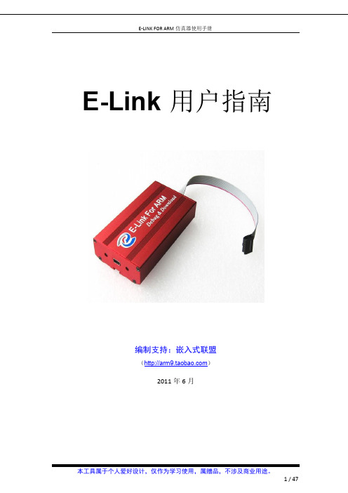
E-Link用户指南编制支持:嵌入式联盟()2011年6月目录1. E-Link ARM JTAG仿真器简介 (3)2. E-LINK驱动安装 (5)3. E-LINK在各个主流开发环境下的设置 (8)3.1. K eilMDK开发环境 (8)3.2. A DS开发环境 (12)3.2.1 E-LINK 在ARM11 (Tiny6410/Mini6410)上的调试 (22)3.3. I AR开发环境下使用E-Link (26)4. J-FLASH ARM使用设置 (36)附录:E-LINK 与 J-LINK V8 对比 (43)1. E-Link FOR ARM仿真器简介E-Link FOR ARM(本文中简称E-Link), 是专为ARM开发设计爱好者调试、仿真以及下载(Debug & download )而推出的JTAG 仿真调试工具。
作为一款专用的ARM JTAG仿真器,E-LINK兼容目前市面大多数JLINK仿真器功能,可配合IAR EWARM,ADS,KEILMDK,WINARM,RealView 等集成开发环境,支持了几乎所有的ARM7/ARM9/ARM11 内核芯片的仿真,通过RDI 接口和各集成开发环境无缝连接,E-LINK突出的亮点之一——支持全自动固件升级,堪称完美地解决了困扰广大学习开发者的固件升级问题。
连接、操作极为方便,易于上手。
E-LINK适用于当前各类主流ARM开发板的仿真调试,是学习开发ARM最具实用价值的开发工具。
可直接使用于各类STM32,2440,6410系列开发板,能够与友善之臂 mini2440/micro2440/ mini6410/Tiny6410,飞凌FL2440/OK6410,华天正Real6410 等产品完美配合。
E-Link 基本介绍如下图所示:* E-LINK 的内部全部采用原装进口芯片,如 CPU,双缓冲,USB口保护电路,ESD ,自动恢复保险丝,包括3.3V电源芯片等; E-LINK的外部结构采用红色铝合金金属外壳。
- 1、下载文档前请自行甄别文档内容的完整性,平台不提供额外的编辑、内容补充、找答案等附加服务。
- 2、"仅部分预览"的文档,不可在线预览部分如存在完整性等问题,可反馈申请退款(可完整预览的文档不适用该条件!)。
- 3、如文档侵犯您的权益,请联系客服反馈,我们会尽快为您处理(人工客服工作时间:9:00-18:30)。
techor ICE™ ARM仿真器用户手册(Version 2.0)深圳技创科技有限公司TECHNIQUE INNOVATOR INC.-© 2003,2004 -第一章概述 (3)1.1 系统配置要求 (3)1.2 设备连接 (4)1.3 电源的使用 (4)1.4 techor ICE™的优点 (4)1.5 内核支持 (5)第二章JTAG口介绍 (6)2.1 接口连接 (6)2.2 接口电平 (7)2.3 TCK信号频率设置 (8)2.4 目标系统设计指南 (9)2.5 RTCK时钟 (10)2.6 JTAG连接转换座 (10)第三章techorICE™介绍 (12)3.1 系统功能层次划分 (12)3.2 软件架构 (12)3.3 远程调试功能 (13)3.4 Server配置 (14)3.4.1自动配置 (14)3.4.2手动配置 (14)3.4.3 IR长度文件 (15)3.4.4配置过程 (16)3.5 多内核目标系统 (16)3.6 系统组成结构 (18)第四章Server program使用指南 (20)4.1 启动Server program (20)4.2Server program菜单介绍 (21)4.2.1工具栏 (21)4.2.2文件菜单 (22)4.2.3视图菜单 (22)4.2.4控制菜单 (23)4.2.5连接菜单 (24)4.2.6设置菜单 (24)4.3Server状态指示 (24)4.3.1配置后的状态 (25)4.3.2连接后的状态 (26)4.3.3激活时的状态 (27)4.4并口设置 (28)4.5时钟设置 (28)4.6运行控制 (29)4.6.1指定各个设备之间的交互方式 (29)4.6.2设置轮询频率 (31)4.7启动选项设置 (32)附录一 TCK频率与设置值转换表 (34)附录二TCK设置值与频率转换表 (37)附录三常见问题 (40)第一章概述本章简单介绍techor ICE™ ARM仿真器的一些基本概念。
系统配置要求设备连接电源的使用techor ICE™的优点内核支持1.1 系统配置要求支持的主机端操作系统:z Windows 95z Windows 98z Windows NTz Windows MEz Windows 2000z Windows XPPC硬件要求:z奔腾233MHz以上CPUz64MB以上内存z200MB以上的硬盘空间z并行端口注意:并口需要在计算机的CMOS中设置好正确的类型后才能正常工作,关于并口设置的相关说明可以参见4.4。
如果使用远程调试功能,计算机还需配置:网卡和相应的驱动程序TCP/IP协议1.2 设备连接图1-1 techor ICE™外观techor ICE™使用标准的25针并口插座与PC机的LPT口相连,到目标板的JTAG接口采用20针IDC宽带线(BT224型)插座。
有的目标板可能使用ARM旧标准的14针JTAG插座,则中间需要一个转换座,2.6专门介绍转换座的使用。
1.3 电源的使用techorICE™采用专用的5V(内正外负)500mA稳压电源供电,这样做的好处是能最大限度地降低目标板与techorICE™之间的相互干预。
JTAG接口数字信号的逻辑电平会随着目标板电源电压的变化而改变。
techorICE™在工作时的一般功耗在0.7W左右。
最大电流不超过300mA。
为了防止异常的电源波动,V2.0版本的techorICE仿真器内部设计了相应的保护电路。
1.4 techor ICE™的优点国内首创的高档内电路:采用高档FPGA+MCU+CPLD方式,逻辑元件与微控器协同工作,故能达到极高的下载速度(120KBytes~200KBytes)和单步执行能力(每秒钟可以单步80次)无限次的Firmware升级能力,通过刷新Firmware(Firmware程序提供免费下载)可以支持ARM的未来核心开放的接口,支持多内核系统,允许调试非ARM核心及DSP核心连接简便,兼容大范围使用电压的目标设备(可以支持低至1.2V的核心电压并在1.2V 到5V间自动适应)除JTAG扫描链以外,不占用目标板上的其他任何资源可编程的JTAG位传送速率(可以设置为5KHz~10MHz),以满足不同调试对象的要求完整实现ARM RDI 1.5和RDI 1.51标准,与ARM Multi-ICE™兼容,支持ARM SDT/ADS/RDS及其他遵从RDI接口标准的调试器,techorICE 支持集成开发调试环境有:9ARM SDT, ADS,RDS9EPI EDB9Green Hills MULTI-20009Intel XScale software toolkit9Mentor Graphics XRAY debugger9IAR EWARM9WinCE Platform Builder9特别支持GNU GDB Debugger调试嵌入式Linux(MontaVista/BlueCat/eCos/中科红旗嵌入式Linux/uClinux/SnapGear)采用ARM集成开发调试环境和techorICE™的配置,支持源代码级调试,ARM THUMB 指令混合编译,支持C、C++、汇编语言的交叉调用,支持ROM断点,多个RAM断点,条件断点,单步执行,随程序同步更新并可即时修改变量、寄存器、内存值。
最多可以支持2个硬件断点,硬件断点可以设置成断点(breakpoint)或者观测点(watchpoint)高速通信的调试功能,高达12Mbps,方便快速下载目标程序和调试程序;支持Flash 在线快速烧写功能(通过自编的脚本文件),可省去通用编程器烧写Flash的麻烦 techorICE™使用标准的25芯并口插座和20针的JTAG插座作为接口,并且提供 14针JTAG转20针JTAG的转换座;特设外部稳压电源供电,正常电压范围4.5V到 5.5V 采用JTAG口的菊花链级联方式,支持同一ASIC内多个不同类型的ARM核techorICE™支持所有ARM内核( ARM7,ARM9,ARM10 )和XScale内核的处理器,包括:Samsung、ATEMEL、Intel、Cirrus Logic、Sharp、Philips、OKI、Motorola、Infineon、NEC、Qualcomm、LSI Logic、Altera、Linkup、Hynix、Winbond、Triscend、Marvell、ZTEIC ZCP320A等等具有ARM内核的通用微处理器和ASIC等 支持多种操作系统:Windows95/98/NT/ME/2000/XP及Linux对ARM有丰富应用经验的工程师提供全方位的技术支持和软硬件参考设计,资深ARM系统设计师与您交流,使您事半功倍!体积轻巧,性能稳定1.5 内核支持当前版本(version 2.0)的techorICE™支持如下所有版本的ARM内核:ARM7全系列:ARM7TDMI /ARM7TDMI-S /ARM7EJ-S /ARM7TDI-S /ARM720T /ARM740T /SecurCore系列(SC100/SC110/SC200/SC210)ARM9全系列:ARM9TDMI /ARM9E-S /ARM9EJ-S /ARM920T /ARM922T /ARM925T /ARM940T /ARM926EJ-S /ARM946E-S /ARM966E-SARM10全系列:ARM1020T / ARM1020E /ARM10200 /ARM10200E /ARM10220E /ARM1022EIntel® XScale 微架构系列:IOP321 PXA210 PXA250 PXA255 IXP425 80200 80321 IR7所有使用上述一个或多个内核的ASIC和目标系统,都能使用techor ICE™来进行调试工作。
第二章JTAG口介绍这一章主要介绍跟techorICE™相关的JTAG接口知识。
具体的JTAG标准和协议,可以查阅IEEE 1149.1协议。
接口连接接口电平TCK信号频率设置目标系统设计指南RTCK时钟JTAG接口转换座2.1 接口连接这部分主要讲述JTAG口的信号功能及应用说明。
下图是JTAG接口的信号排列示意图:图2-1 JTAG口的信号排列图接口是一个20脚的IDC插座。
下表给出了具体的信号说明:引脚信号名相对仿真器的信号方向信号描述1 VTref 输入接口电平参考电压,通常可直接接电源2 Vsupply 输入电源3 nTRST 输出 TargetJTAG口复位-在目标端应当做上拉处理以防误复位4 GND -- 地5 TDI 输出 TestDataIn-从仿真器输出到目标板,目标板端应当做上拉或者下拉处理6 GND -- 地7 TMS 输出Test Mode Signal-目标板端应当做上拉处理8 GND -- 地9 TCK 输出 TestClock-目标板端应当做上拉或者下拉处理10 GND -- 地11 RTCK 输入 ReturnTestClock-由目标端反馈给仿真器的时钟信号,用来同步TCK信号的产生。
不使用时可以直接接地12 GND -- 地13 TDO 输入Test Data Out-14 GND -- 地15 nSRST 输出/输入Target System Reset-与目标板上的系统复位信号相连。
可以直接对目标系统复位,同时可以检测目标系统的复位情况。
为了防止误触发,目标板端应当做上拉处理16 GND -- 地17 DBGRQ -- 调试ARM内核时不使用18 GND -- 地19 DBGACK-- 调试ARM内核时不使用20 GND -- 地表2-1 JTAG引脚说明2.2 接口电平techorICE™推荐的正常使用电压为2.5 – 5.0V,最大不超过2.0 – 5.5V。
随着电源电压的变化,接口的逻辑高电平和判决门限电平都将随之变化,这使得techorICE™能够与不同电压的目标系统在逻辑上兼容。
下面一张图显示了这种变化关系:图2-2接口逻辑电平变化关系V oh是指techorICE™的输出逻辑高电平。
V i (th) 是输入信号的逻辑判决门限电平。
这两者之间存在下述关系:Vi (th) = 1/2(Voh)2.3 TCK信号频率设置为了与不同速率的目标对象相兼容,JTAG口的通信速率应调整到一个合适的水平。
数据传输速率是由TCK信号的频率来决定的,有两种方法可以调节TCK信号的频率。
(1) 在Server program中手动设置打开菜单设置->JTAG设置,在对应的栏中填入要求的数值。