CXSJM6P-20资料下载
SM320C6201BGLPS20中文资料
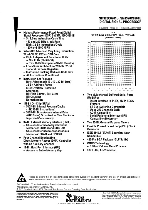
SM320C6201B, SMJ320C6201B DIGITAL SIGNAL PROCESSOR
SGUS031B – APRIL 2000 – REVISED AUGUST 2001
D Highest Performance Fixed-Point Digital
Copyright 2001, Texas Instruments Incorporated
On products compliant to MILĆPRFĆ38535, all parameters are tested unless otherwise noted. On all other products, production processing does not necessarily include testing of all parameters.
AA Y W V U T R P N M L K J H G F E D C B A
GLP 429-PIN BALL GRID ARRAY (BGA) PACKAGE (BOTTOM VIEW)
D
D
1 2
3 4
5 6
7 8
9 10
11 12
13 14
15 16
17 18
19 20
21
D Two Multichannel Buffered Serial Ports
description . . . . . . . . . . . . . . . . . . . . . . . . . . . . . . . . . . . . . . . . . 2 device characteristics . . . . . . . . . . . . . . . . . . . . . . . . . . . . . . . . 3 functional block diagram . . . . . . . . . . . . . . . . . . . . . . . . . . . . . . 3 CPU description . . . . . . . . . . . . . . . . . . . . . . . . . . . . . . . . . . . . . 4 signal groups description . . . . . . . . . . . . . . . . . . . . . . . . . . . . . 7 signal descriptions . . . . . . . . . . . . . . . . . . . . . . . . . . . . . . . . . . . 9 development support . . . . . . . . . . . . . . . . . . . . . . . . . . . . . . . . 22 device and development support nomenclature . . . . . . . . . 23 documentation support . . . . . . . . . . . . . . . . . . . . . . . . . . . . . . 24 clock PLL . . . . . . . . . . . . . . . . . . . . . . . . . . . . . . . . . . . . . . . . . 26 power-supply sequencing . . . . . . . . . . . . . . . . . . . . . . . . . . . . 27 absolute maximum ratings over operating case temperature ranges . . . . . . . . . . . . . . . . . . . . . . . . . . . . 28 recommended operating conditions . . . . . . . . . . . . . . . . . . . 28 electrical characteristics over recommended ranges of supply voltage and operating case temperature . . . . 29 parameter measurement information . . . . . . . . . . . . . . . 30 signal transition levels . . . . . . . . . . . . . . . . . . . . . . . . . . . . input and output clocks . . . . . . . . . . . . . . . . . . . . . . . . . . . asynchronous memory timing . . . . . . . . . . . . . . . . . . . . . synchronous-burst memory timing . . . . . . . . . . . . . . . . . synchronous DRAM timing . . . . . . . . . . . . . . . . . . . . . . . . HOLD/HOLDA timing . . . . . . . . . . . . . . . . . . . . . . . . . . . . reset timing . . . . . . . . . . . . . . . . . . . . . . . . . . . . . . . . . . . . . external interrupt timing . . . . . . . . . . . . . . . . . . . . . . . . . . host-port interface timing . . . . . . . . . . . . . . . . . . . . . . . . . multichannel buffered serial port timing . . . . . . . . . . . . . DMAC, timer, power-down timing . . . . . . . . . . . . . . . . . . JTAG test-port timing . . . . . . . . . . . . . . . . . . . . . . . . . . . . mechanical data . . . . . . . . . . . . . . . . . . . . . . . . . . . . . . . . . 30 31 34 36 40 44 45 47 48 51 59 60 61
SPP20N60元件参数

Marking 20N60S5 20N60S5
Maximum Ratings
Parameter
Symbol
Continuous drain current
ID
TC = 25 °C
TC = 100 °C
Pulsed drain current, tp limited by Tjmax
ID puls
Avalanche energy, single pulse
-
t d(off)
-
120 - ns
25
-
140 210
Fall time
tf
-
30 45
Gate Charge Characteristics
Gate to source charge
Qgs
VDD=350V, ID=20A
Gate to drain charge
Qgd
Gate charge total
0.012 0.091
Unit Ws/K
Ptot (t)
Tj R th1
C th 1
C th 2
Rth,n Tcase External Heatsink
C th ,n
Tamb
Rev. 2.1
Page 4
2004-03-30
SPP20N60S5 SPB20N60S5
1 Power dissipation Ptot = f (TC)
Symbol dv/dt
Value 20
Unit V/ns
Symbol RthJC RthJA
Tsold
Values
Unit
min. typ. max.
-
corex cxdn6s0521 非隔离dc-dc模块-用户手册说明书
非隔离DC-DC模块CXDN6S0521产品说明书V1.001产品概述CXDN6S0521是非隔离型DC-DC电源模块,采用双面表贴结构和同步整流技术,占用的PCB面积仅为标准面积的一半。
在空间性能和成本受限的产品中该模块是一个理想的选择。
1.1产品特性◆可实现与TI公司的PTH05000W脚对脚替换◆输入电压范围:5.0V(4.5V~5.5V)◆输出电压范围:0.9V~3.3V◆最大输出电流:6.0A◆效率:91%(满载条件)◆输入欠压保护◆输出过流保护◆预偏置启动能力◆过温保护◆双面表贴结构1.2管脚排列图1管脚排列图引出端管脚说明:1.3功能框图该模块包括开/关抑制,输出电压调整(微调),输出电流限制和真正意义上的过温度保护。
为了实现高的转换效率,本模块输出侧使用了同步整流技术。
其输出预偏置性能能够保证在启动期间输出端不会吸入电流。
Vo Adj图2功能框图2电特性2.1绝对最大额定值2.2推荐工作条件2.3电特性若无特殊说明,测试条件为T A = -40℃~+85℃,V I = 5.0V,V O = 3.3V, C IN = 330μF,C OUT = 100μF。
3应用信息3.1典型应用注:R SET =(12VOUT−0.6-2.21)kΩ图3典型应用电路图3.2输出电压设置通过RSET 设置输出电压值,R SET =(12VOUT−0.6-2.21)kΩ,下表列出典型的输出电3.3操作规程及注意事项模块必须采取防静电措施进行操作。
取用模块时应佩戴防静电手套,防止ESD对模块造成损伤。
将模块插入电路板上的底座时,应注意模块的方向,防止插反;将模块从电路板上的底座取出时,应注意施力方向以确保模块管脚均匀受力。
推荐下列操作措施:a) 模块应在防静电的工作台上操作,或佩戴防静电手套;b) 试验设备和器具应做好接地处理;c) 不能随意触摸模块表面及引线;d) 模块应存放在导电材料制成的容器中(如:集成电路专用盒);e) 生产、测试、使用以及转运过程中应避免使用引起静电的塑料、橡胶或丝织物;f) 相对湿度尽可能保持在50%以上;g) 使用时,正确区分模块的电源和地,防止发生短路。
PM10CSJ060中文资料
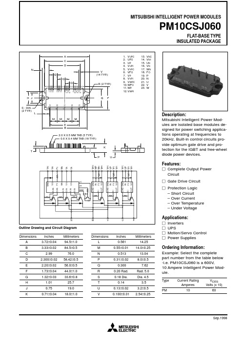
G
F
S - DIA. (2 TYP.)
P
L M M E B 2.0 X 0.5 MM TAB (5 TYP.) 0.6 X 0.4 MM TAB (18 TYP.) K M M
T P
VWPC WP WFO VWPI V NC
U
VUPC UP UFO VUPI VVPC VP VFO VVPI
P
V N1
WN
FO
VN
UN
GND GND IN SI FO OUT V CC
GND GND IN SI FO OUT V CC
TB
GND
GND GND IN SI FO OUT V CC
GND
V CC
WN
VN
S WN
O WN
S UN
UN
FO
TC
O UN
S VN
O VN
N
W
V
U
Outline Drawing and Circuit Diagram Dimensions A B C D E F G H J K Inches 3.72±0.04 3.33±0.02 2.99 2.300±0.02 2.20±0.02 1.73±0.04 1.32±0.03 1.01 0.75 0.71±0.04 Millimeters 94.5±1.0 84.5±0.5 76.0 58.42±0.5 56.0±0.5 44.0±1.0 33.6±0.8 25.7 19.0 18.0±1.0 Dimensions L M N P Q R S T U V Inches 0.561 0.55±0.01 0.513 0.31±0.02 0.300 0.20 Rad. 0.18 Dia. 0.14 0.13±0.02 0.100±0.01 Millimeters 14.25 14.0±0.25 13.04 8.0±0.5 7.62 Rad. 5.0 Dia. 4.5 3.5 3.2±0.5 2.54±0.25
电网保护-Sepam 20系列
19
说明
20
预定义功能说明
21
使用SFT2841 软件调整预定义功能
22
特性
22
基本单元
22
描述
23
说明
26
尺寸
27
技术特性
28
环境特性
29
接线图
29
基本单元
29
Sepam 20系列
30
Sepam 40系列
31
相电流输入
32
剩余电流输入
33
电压输入
33
Sepam 20系列
34
Sepam 40系列
35
1A至6250A
-
220V至250kV
Sepam 40系列
1A至6250A 0.4至1.3 In 见In额定相电流 2A,5A或20A额定值
1A至6250A (In0 = In)
1A至6250A (In0 = In/10)
220V至250kV
3VTs: V1, V2, V3 2VTs: U21, U32 1VT: V1
Sepam 20系列传感器输入
相电流输入 剩余电流输入 相电压输入 剩余电压输入 温度输入 (在MET148-2模块上)
S20
3 1 0 0 0
T20, M20
3 1 0 0 8
B21, B22
0 0 3 1 0
Sepam 40系列传感器输入
相电流输入 上)
42
10输入/4输出模块
42
描述
43
安装
44
Sepam 20系列的逻辑输入/ 输出分配
45
Sepam 40系列的逻辑输入/ 输出分配
46
沛城4820通信铁锂BMS规格书P16S20A-4435-29

BMS产品规格书目录1. 简介 (5)2. 功能特性 (5)3. 功能示意框图 (6)4. 电气特性 (6)4.1 基本参数设置 (6)4.2 LED指示说明 (8)4.3 蜂鸣器动作说明 (9)4.4 按键说明 (9)4.5 休眠及唤醒 (9)5 通信说明 (10)5.1 RS232通信 (10)5.2 RS485通信 (10)5.3 拨码开关设置 (10)6 接口定义 (11)6.1 接口图示 (11)6.2 电气接口定义 (12)6.3 安装连接说明 (13)7 实物图和尺寸图 (13)8 使用注意事项 (14)1.简介随着锂电池在通信行业的广泛应用,对电池管理系统也提出了高性能、高可靠性及高性价比等要求。
本产品是专门针对基站后备电池设计的BMS,采用集成化的设计将采集、管理、通信等功能集成于一体。
可广泛应用在室内室外基站,如一体化基站、边际站、直放站、宏基站、太阳能基站等。
2.功能特性●具有单体电压、总体电压检测,过充、过放告警及保护功能。
常温下静态电压采样精度可达≤20mV。
●具有充、放电电流检测,充、放电过流告警及保护功能。
充电电流显示为正,放电电流显示为负,常温下电流采样精度可达≤2%@FS。
●具有电芯温度检测,电芯高、低温告警及保护功能,常温下温度采样精度可达≤3℃。
●短路保护功能。
●具有充电均衡功能。
●电芯容量估算功能。
电池组满充容量、当前容量、设计容量可以通过上位机进行设置,在进行完整充放电循环后容量可自动更新。
●LED状态指示功能。
●上位机软件控制功能,可通过上位机软件方便地对过充、过放、充放电过流、过温、欠温等保护参数,容量、休眠、均衡等参数进行设置。
●RS232通信功能,采用隔离通信。
●RS485通信功能,采用隔离通信。
3. 功能示意框图4. 电气特性4.1基本参数设置 (注:以下参数除特殊注明以外,25℃环温下测试)指示说明表1 LED工作状态指示表2 容量指示说明表3 LED闪动说明备注:可通过上位机使能或禁止LED指示灯告警,出厂默认为使能的。
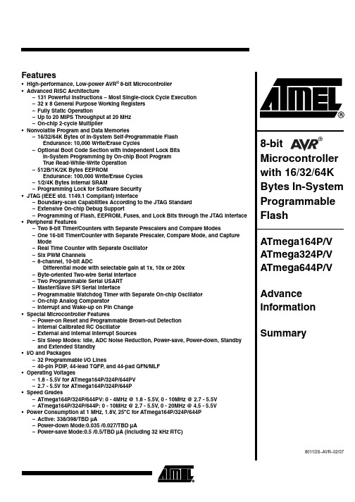
ATMEGA644P-20MU中文资料
Features•High-performance, Low-power AVR® 8-bit Microcontroller •Advanced RISC Architecture–131 Powerful Instructions – Most Single-clock Cycle Execution –32 x 8 General Purpose Working Registers–Fully Static Operation–Up to 20 MIPS Throughput at 20 MHz–On-chip 2-cycle Multiplier•Nonvolatile Program and Data Memories–16/32/64K Bytes of In-System Self-Programmable FlashEndurance: 10,000 Write/Erase Cycles–Optional Boot Code Section with Independent Lock BitsIn-System Programming by On-chip Boot ProgramTrue Read-While-Write Operation–512B/1K/2K Bytes EEPROMEndurance: 100,000 Write/Erase Cycles–1/2/4K Bytes Internal SRAM–Programming Lock for Software Security•JTAG (IEEE std. 1149.1 Compliant) Interface–Boundary-scan Capabilities According to the JTAG Standard–Extensive On-chip Debug Support–Programming of Flash, EEPROM, Fuses, and Lock Bits through the JTAG Interface •Peripheral Features–Two 8-bit Timer/Counters with Separate Prescalers and Compare Modes–One 16-bit Timer/Counter with Separate Prescaler, Compare Mode, and Capture Mode–Real Time Counter with Separate Oscillator–Six PWM Channels–8-channel, 10-bit ADCDifferential mode with selectable gain at 1x, 10x or 200x–Byte-oriented Two-wire Serial Interface–Two Programmable Serial USART–Master/Slave SPI Serial Interface–Programmable Watchdog Timer with Separate On-chip Oscillator–On-chip Analog Comparator–Interrupt and Wake-up on Pin Change•Special Microcontroller Features–Power-on Reset and Programmable Brown-out Detection–Internal Calibrated RC Oscillator–External and Internal Interrupt Sources–Six Sleep Modes: Idle, ADC Noise Reduction, Power-save, Power-down, Standby and Extended Standby•I/O and Packages–32 Programmable I/O Lines–40-pin PDIP, 44-lead TQFP, and 44-pad QFN/MLF•Operating Voltages–1.8 - 5.5V for ATmega164P/324P/644PV–2.7 - 5.5V for ATmega164P/324P/644P•Speed Grades–ATmega164P/324P/644PV: 0 - 4MHz @ 1.8 - 5.5V, 0 - 10MHz @ 2.7 - 5.5V–ATmega164P/324P/644P: 0 - 10MHz @ 2.7 - 5.5V, 0 - 20MHz @ 4.5 - 5.5V•Power Consumption at 1 MHz, 1.8V, 25°C for ATmega164P/324P/644P –Active: 338/398/TBD µA–Power-down Mode:0.035 /0.027/TBD µA–Power-save Mode:0.5 /0.5/TBD µA (Including 32 kHz RTC)8-bit Microcontrollerwith 16/32/64K Bytes In-System ProgrammableATmega164P/V ATmega324P/V ATmega644P/V28011DS–AVR–02/07ATmega164P/324P/644P1.Pin ConfigurationsFigure 1-1.Pinout ATmega164P/324P/644PNote:The large center pad underneath the QFN/MLF package should be soldered to ground on theboard to ensure good mechanical stability.38011DS–AVR–02/07ATmega164P/324P/644P1.1DisclaimerTypical values contained in this datasheet are based on simulations and characterization of other AVR microcontrollers manufactured on the same process technology. Min and Max values will be available after the device is characterized.48011DS–AVR–02/07ATmega164P/324P/644P2.OverviewThe ATmega164P/324P/644P is a low-power CMOS 8-bit microcontroller based on the AVR enhanced RISC architecture. By executing powerful instructions in a single clock cycle, the ATmega164P/324P/644P achieves throughputs approaching 1 MIPS per MHz allowing the sys-tem designer to optimize power consumption versus processing speed.2.1Block DiagramFigure 2-1.Block DiagramThe AVR core combines a rich instruction set with 32 general purpose working registers. All the 32 registers are directly connected to the Arithmetic Logic Unit (ALU), allowing two independent registers to be accessed in one single instruction executed in one clock cycle. The resulting architecture is more code efficient while achieving throughputs up to ten times faster than con-ventional CISC microcontrollers.58011DS–AVR–02/07ATmega164P/324P/644PThe ATmega164P/324P/644P provides the following features: 16/32/64K bytes of In-System Programmable Flash with Read-While-Write capabilities, 512B/1K/2K bytes EEPROM, 1/2/4K bytes SRAM, 32 general purpose I/O lines, 32 general purpose working registers, Real Time Counter (RTC), three flexible Timer/Counters with compare modes and PWM, 2 USARTs, a byte oriented 2-wire Serial Interface, a 8-channel, 10-bit ADC with optional differential input stage with programmable gain, programmable Watchdog Timer with Internal Oscillator, an SPI serial port, IEEE std. 1149.1 compliant JTAG test interface, also used for accessing the On-chip Debug system and programming and six software selectable power saving modes. The Idle mode stops the CPU while allowing the SRAM, Timer/Counters, SPI port, and interrupt system to continue functioning. The Power-down mode saves the register contents but freezes the Oscillator, disabling all other chip functions until the next interrupt or Hardware Reset. In Power-save mode, the asynchronous timer continues to run, allowing the user to maintain a timer base while the rest of the device is sleeping. The ADC Noise Reduction mode stops the CPU and all I/O modules except Asynchronous Timer and ADC, to minimize switching noise during ADC conversions. In Standby mode, the Crystal/Resonator Oscillator is running while the rest of the device is sleeping. This allows very fast start-up combined with low power consumption. In Extended Standby mode, both the main Oscillator and the Asynchronous Timer continue to run.The device is manufactured using Atmel’s high-density nonvolatile memory technology. The On-chip ISP Flash allows the program memory to be reprogrammed in-system through an SPI serial interface, by a conventional nonvolatile memory programmer, or by an On-chip Boot program running on the AVR core. The boot program can use any interface to download the application program in the application Flash memory. Software in the Boot Flash section will continue to run while the Application Flash section is updated, providing true Read-While-Write operation. By combining an 8-bit RISC CPU with In-System Self-Programmable Flash on a monolithic chip,the Atmel ATmega164P/324P/644P is a powerful microcontroller that provides a highly flexible and cost effective solution to many embedded control applications.The ATmega164P/324P/644P AVR is supported with a full suite of program and system devel-opment tools including: C compilers, macro assemblers, program debugger/simulators, in-circuit emulators, and evaluation kits.2.2Comparison Between ATmega164P, ATmega324P and ATmega644P2.3Pin Descriptions2.3.1VCCDigital supply voltage.2.3.2GNDGround.Table 2-1.Differences between ATmega164P and ATmega644PDevice Flash EEPROM RAM A Tmega164P 16 Kbyte 512 Bytes 1 Kbyte A Tmega324P 32 Kbyte 1 Kbyte 2 Kbyte A Tmega644P64 Kbyte2 Kbyte4 Kbyte68011DS–AVR–02/07ATmega164P/324P/644P2.3.3Port A (PA7:PA0)Port A serves as analog inputs to the Analog-to-digital Converter.Port A also serves as an 8-bit bi-directional I/O port with internal pull-up resistors (selected for each bit). The Port A output buffers have symmetrical drive characteristics with both high sink and source capability. As inputs, Port A pins that are externally pulled low will source current if the pull-up resistors are activated. The Port A pins are tri-stated when a reset condition becomes active, even if the clock is not running.Port A also serves the functions of various special features of the ATmega164P/324P/644P as listed on page 79.2.3.4Port B (PB7:PB0)Port B is an 8-bit bi-directional I/O port with internal pull-up resistors (selected for each bit). The Port B output buffers have symmetrical drive characteristics with both high sink and source capability. As inputs, Port B pins that are externally pulled low will source current if the pull-up resistors are activated. The Port B pins are tri-stated when a reset condition becomes active,even if the clock is not running.Port B also serves the functions of various special features of the ATmega164P/324P/644P as listed on page 81.2.3.5Port C (PC7:PC0)Port C is an 8-bit bi-directional I/O port with internal pull-up resistors (selected for each bit). The Port C output buffers have symmetrical drive characteristics with both high sink and source capability. As inputs, Port C pins that are externally pulled low will source current if the pull-up resistors are activated. The Port C pins are tri-stated when a reset condition becomes active,even if the clock is not running.Port C also serves the functions of the JTAG interface, along with special features of the ATmega164P/324P/644P as listed on page 84.2.3.6Port D (PD7:PD0)Port D is an 8-bit bi-directional I/O port with internal pull-up resistors (selected for each bit). The Port D output buffers have symmetrical drive characteristics with both high sink and source capability. As inputs, Port D pins that are externally pulled low will source current if the pull-up resistors are activated. The Port D pins are tri-stated when a reset condition becomes active,even if the clock is not running.Port D also serves the functions of various special features of the ATmega164P/324P/644P as listed on page 86.2.3.7RESETReset input. A low level on this pin for longer than the minimum pulse length will generate a reset, even if the clock is not running. The minimum pulse length is given in Table 9-1 on page 50. Shorter pulses are not guaranteed to generate a reset.2.3.8XTAL1Input to the inverting Oscillator amplifier and input to the internal clock operating circuit.78011DS–AVR–02/07ATmega164P/324P/644P2.3.9XTAL2Output from the inverting Oscillator amplifier.2.3.10AVCCAVCC is the supply voltage pin for Port F and the Analog-to-digital Converter. It should be exter-nally connected to V CC , even if the ADC is not used. If the ADC is used, it should be connected to V CC through a low-pass filter.2.3.11AREFThis is the analog reference pin for the Analog-to-digital Converter.3.ResourcesA comprehensive set of development tools, application notes and datasheetsare available for download on /avr.88011DS–AVR–02/07ATmega164P/324P/644P4.Register SummaryAddressNameBit 7Bit 6Bit 5Bit 4Bit 3Bit 2Bit 1Bit 0Page(0xFF)Reserved -------(0xFE)Reserved --------(0xFD)Reserved --------(0xFC)Reserved --------(0xFB)Reserved -------(0xFA)Reserved --------(0xF9)Reserved -------(0xF8)Reserved --------(0xF7)Reserved --------(0xF6)Reserved --------(0xF5)Reserved -------(0xF4)Reserved --------(0xF3)Reserved --------(0xF2)Reserved --------(0xF1)Reserved -------(0xF0)Reserved --------(0xEF)Reserved -------(0xEE)Reserved --------(0xED)Reserved --------(0xEC)Reserved --------(0xEB)Reserved -------(0xEA)Reserved --------(0xE9)Reserved --------(0xE8)Reserved --------(0xE7)Reserved -------(0xE6)Reserved --------(0xE5)Reserved --------(0xE4)Reserved --------(0xE3)Reserved -------(0xE2)Reserved --------(0xE1)Reserved -------(0xE0)Reserved -------(0xDF)Reserved --------(0xDE)Reserved --------(0xDD)Reserved --------(0xDC)Reserved -------(0xDB)Reserved --------(0xDA)Reserved --------(0xD9)Reserved --------(0xD8)Reserved --------(0xD7)Reserved --------(0xD6)Reserved --------(0xD5)Reserved --------(0xD4)Reserved --------(0xD3)Reserved --------(0xD2)Reserved --------(0xD1)Reserved --------(0xD0)Reserved --------(0xCF)Reserved --------(0xCE)UDR1 USART1 I/O Data Register184(0xCD)UBRR1H ----USART1 Baud Rate Register High Byte189/201(0xCC)UBRR1L USART1 Baud Rate Register Low Byte189/201(0xCB)Reserved --------(0xCA)UCSR1C UMSEL11UMSEL10UPM11UPM10USBS1UCSZ11UCSZ10UCPOL1187/200(0xC9)UCSR1B RXCIE1TXCIE1UDRIE1RXEN1TXEN1UCSZ12RXB81TXB81186/200(0xC8)UCSR1A RXC1TXC1UDRE1FE1DOR1UPE1U2X1MPCM1185/199(0xC7)Reserved --------(0xC6)UDR0 USART0 I/O Data Register 184(0xC5)UBRR0H ----USART0 Baud Rate Register High Byte189/201(0xC4)UBRR0L USART0 Baud Rate Register Low Byte189/201(0xC3)Reserved --------(0xC2)UCSR0C UMSEL01UMSEL00UPM01UPM00USBS0UCSZ01UCSZ00UCPOL0187/200(0xC1)UCSR0B RXCIE0TXCIE0UDRIE0RXEN0TXEN0UCSZ02RXB80TXB80186/200(0xC0)UCSR0ARXC0TXC0UDRE0FE0DOR0UPE0U2X0MPCM0185/19998011DS–AVR–02/07ATmega164P/324P/644P(0xBF)Reserved --------(0xBE)Reserved --------(0xBD)TWAMR TWAM6TWAM5TWAM4TWAM3TWAM2TWAM1TWAM0-232(0xBC)TWCR TWINT TWEA TWSTA TWSTO TWWC TWEN -TWIE 228(0xBB)TWDR 2-wire Serial Interface Data Register230(0xBA)TWAR TWA6TWA5TWA4TWA3TWA2TWA1TWA0TWGCE 232(0xB9)TWSR TWS7TWS6TWS5TWS4TWS3-TWPS1TWPS0230(0xB8)TWBR 2-wire Serial Interface Bit Rate Register228(0xB7)Reserved --------(0xB6)ASSR -EXCLK AS2TCN2UBOCR2AUBOCR2BUBTCR2AUBTCR2BUB153(0xB5)Reserved --------(0xB4)OCR2B Timer/Counter2 Output Compare Register B 152(0xB3)OCR2A Timer/Counter2 Output Compare Register A152(0xB2)TCNT2 Timer/Counter2 (8 Bit)152(0xB1)TCCR2B FOC2A FOC2B --WGM22CS22CS21CS20151(0xB0)TCCR2A COM2A1COM2A0COM2B1COM2B0--WGM21WGM20148(0xAF)Reserved --------(0xAE)Reserved --------(0xAD)Reserved --------(0xAC)Reserved --------(0xAB)Reserved --------(0xAA)Reserved --------(0xA9)Reserved --------(0xA8)Reserved --------(0xA7)Reserved --------(0xA6)Reserved --------(0xA5)Reserved --------(0xA4)Reserved --------(0xA3)Reserved --------(0xA2)Reserved --------(0xA1)Reserved --------(0xA0)Reserved --------(0x9F)Reserved --------(0x9E)Reserved --------(0x9D)Reserved --------(0x9C)Reserved --------(0x9B)Reserved --------(0x9A)Reserved --------(0x99)Reserved --------(0x98)Reserved --------(0x97)Reserved --------(0x96)Reserved --------(0x95)Reserved --------(0x94)Reserved --------(0x93)Reserved --------(0x92)Reserved --------(0x91)Reserved --------(0x90)Reserved --------(0x8F)Reserved --------(0x8E)Reserved --------(0x8D)Reserved --------(0x8C)Reserved --------(0x8B)OCR1BH Timer/Counter1 - Output Compare Register B High Byte 134 (0x8A)OCR1BL Timer/Counter1 - Output Compare Register B Low Byte 134(0x89)OCR1AH Timer/Counter1 - Output Compare Register A High Byte 134(0x88)OCR1AL Timer/Counter1 - Output Compare Register A Low Byte 134(0x87)ICR1H Timer/Counter1 - Input Capture Register High Byte 135(0x86)ICR1L Timer/Counter1 - Input Capture Register Low Byte 135(0x85)TCNT1H Timer/Counter1 - Counter Register High Byte 134(0x84)TCNT1L Timer/Counter1 - Counter Register Low Byte134(0x83)Reserved --------(0x82)TCCR1C FOC1A FOC1B ------133(0x81)TCCR1B ICNC1ICES1-WGM13WGM12CS12CS11CS10132(0x80)TCCR1A COM1A1COM1A0COM1B1COM1B0--WGM11WGM10130(0x7F)DIDR1------AIN1D AIN0D 235(0x7E)DIDR0ADC7DADC6DADC5DADC4DADC3DADC2DADC1DADC0D255AddressNameBit 7Bit 6Bit 5Bit 4Bit 3Bit 2Bit 1Bit 0Page108011DS–AVR–02/07ATmega164P/324P/644P(0x7D)Reserved --------(0x7C)ADMUX REFS1REFS0ADLAR MUX4MUX3MUX2MUX1MUX0251(0x7B)ADCSRB -ACME ---ADTS2ADTS1ADTS0233(0x7A)ADCSRA ADENADSCADATEADIFADIEADPS2ADPS1ADPS0252(0x79)ADCH ADC Data Register High byte 254(0x78)ADCL ADC Data Register Low byte254(0x77)Reserved --------(0x76)Reserved --------(0x75)Reserved --------(0x74)Reserved --------(0x73)PCMSK3PCINT31PCINT30PCINT29PCINT28PCINT27PCINT26PCINT25PCINT2469(0x72)Reserved --------(0x71)Reserved --------(0x70)TIMSK2-----OCIE2B OCIE2A TOIE2155(0x6F)TIMSK1--ICIE1--OCIE1B OCIE1A TOIE1135(0x6E)TIMSK0-----OCIE0B OCIE0A TOIE0107(0x6D)PCMSK2PCINT23PCINT22PCINT21PCINT20PCINT19PCINT18PCINT17PCINT1669(0x6C)PCMSK1PCINT15PCINT14PCINT13PCINT12PCINT11PCINT10PCINT9PCINT869(0x6B)PCMSK0PCINT7PCINT6PCINT5PCINT4PCINT3PCINT2PCINT1PCINT070(0x6A)Reserved --------(0x69)EICRA --ISC21ISC20ISC11ISC10ISC01ISC0066(0x68)PCICR ----PCIE3PCIE2PCIE1PCIE068(0x67)Reserved --------(0x66)OSCCAL Oscillator Calibration Register39(0x65)Reserved --------(0x64)PRR PRTWI PRTIM2PRTIM0PRUSART1PRTIM1PRSPI PRUSART0PRADC47(0x63)Reserved --------(0x62)Reserved --------(0x61)CLKPR CLKPCE ---CLKPS3CLKPS2CLKPS1CLKPS039(0x60)WDTCSR WDIF WDIE WDP3WDCE WDE WDP2WDP1WDP0580x3F (0x5F)SREG I T H S V N Z C 120x3E (0x5E)SPH SP15SP14SP13SP12SP11SP10SP9SP8120x3D (0x5D)SPL SP7SP6SP5SP4SP3SP2SP1SP0120x3C (0x5C)Reserved --------0x3B (0x5B)RAMPZ -------RAMPZ0150x3A (0x5A)Reserved --------0x39 (0x59)Reserved --------0x38 (0x58)Reserved --------0x37 (0x57)SPMCSR SPMIE RWWSBSIGRD RWWSREBLBSETPGWRTPGERSSPMEN2770x36 (0x56)Reserved --------0x35 (0x55)MCUCR JTD BODS BODSEPUD --IVSEL IVCE 78/2650x34 (0x54)MCUSR ---JTRF WDRF BORF EXTRF PORF 53/2660x33 (0x53)SMCR ----SM2SM1SM0SE 460x32 (0x52)Reserved --------0x31 (0x51)OCDR On-Chip Debug Register2610x30 (0x50)ACSR ACD ACBG ACO ACI ACIE ACIC ACIS1ACIS02520x2F (0x4F)Reserved --------0x2E (0x4E)SPDR SPI 0 Data Register1650x2D (0x4D)SPSR SPIF0WCOL0-----SPI2X01650x2C (0x4C)SPCR SPIE0SPE0DORD0MSTR0CPOL0CPHA0SPR01SPR001630x2B (0x4B)GPIOR2General Purpose I/O Register 2270x2A (0x4A)GPIOR1General Purpose I/O Register 1270x29 (0x49)Reserved --------0x28 (0x48)OCR0B Timer/Counter0 Output Compare Register B 1070x27 (0x47)OCR0A Timer/Counter0 Output Compare Register A1070x26 (0x46)TCNT0 Timer/Counter0 (8 Bit)1070x25 (0x45)TCCR0B FOC0A FOC0B --WGM02CS02CS01CS001060x24 (0x44)TCCR0A COM0A1COM0A0COM0B1COM0B0--WGM01WGM001070x23 (0x43)GTCCR TSM -----PSR2PSR543101570x22 (0x42)EEARH ----EEPROM Address Register High Byte220x21 (0x41)EEARL EEPROM Address Register Low Byte220x20 (0x40)EEDR EEPROM Data Register220x1F (0x3F)EECR --EEPM1EEPM0EERIE EEMWE EEWE EERE 230x1E (0x3E)GPIOR0General Purpose I/O Register 0280x1D (0x3D)EIMSK -----INT2INT1INT0670x1C (0x3C)EIFR-----INTF2INTF1INTF067AddressNameBit 7Bit 6Bit 5Bit 4Bit 3Bit 2Bit 1Bit 0PageATmega164P/324P/644PAddress Name Bit 7Bit 6Bit 5Bit 4Bit 3Bit 2Bit 1Bit 0Page 0x1B (0x3B)PCIFR----PCIF3PCIF2PCIF1PCIF068 0x1A (0x3A)Reserved--------0x19 (0x39)Reserved--------0x18 (0x38)Reserved--------0x17 (0x37)TIFR2-----OCF2b OCF2A TOV2156 0x16 (0x36)TIFR1--ICF1--OCF1B OCF1A TOV1136 0x15 (0x35)TIFR0-----OCF0B OCF0A TOV0108 0x14 (0x34)Reserved--------0x13 (0x33)Reserved--------0x12 (0x32)Reserved--------0x11 (0x31)Reserved--------0x10 (0x30)Reserved--------0x0F (0x2F)Reserved--------0x0E (0x2E)Reserved--------0x0D (0x2D)Reserved--------0x0C (0x2C)Reserved--------0x0B (0x2B)PORTD PORTD7PORTD6PORTD5PORTD4PORTD3PORTD2PORTD1PORTD091 0x0A (0x2A)DDRD DDD7DDD6DDD5DDD4DDD3DDD2DDD1DDD091 0x09 (0x29)PIND PIND7PIND6PIND5PIND4PIND3PIND2PIND1PIND091 0x08 (0x28)PORTC PORTC7PORTC6PORTC5PORTC4PORTC3PORTC2PORTC1PORTC090 0x07 (0x27)DDRC DDC7DDC6DDC5DDC4DDC3DDC2DDC1DDC090 0x06 (0x26)PINC PINC7PINC6PINC5PINC4PINC3PINC2PINC1PINC091 0x05 (0x25)PORTB PORTB7PORTB6PORTB5PORTB4PORTB3PORTB2PORTB1PORTB090 0x04 (0x24)DDRB DDB7DDB6DDB5DDB4DDB3DDB2DDB1DDB090 0x03 (0x23)PINB PINB7PINB6PINB5PINB4PINB3PINB2PINB1PINB090 0x02 (0x22)PORTA PORTA7PORTA6PORTA5PORTA4PORTA3PORTA2PORTA1PORTA090 0x01 (0x21)DDRA DDA7DDA6DDA5DDA4DDA3DDA2DDA1DDA090 0x00 (0x20)PINA PINA7PINA6PINA5PINA4PINA3PINA2PINA1PINA090 Notes: 1.For compatibility with future devices, reserved bits should be written to zero if accessed. Reserved I/O memory addresses should never be written.2.I/O registers within the address range $00 - $1F are directly bit-accessible using the SBI and CBI instructions. In these reg-isters, the value of single bits can be checked by using the SBIS and SBIC instructions.3.Some of the status flags are cleared by writing a logical one to them. Note that the CBI and SBI instructions will operate onall bits in the I/O register, writing a one back into any flag read as set, thus clearing the flag. The CBI and SBI instructionswork with registers 0x00 to 0x1F only.4.When using the I/O specific commands IN and OUT, the I/O addresses $00 - $3F must be used. When addressing I/O regis-ters as data space using LD and ST instructions, $20 must be added to these addresses. The A Tmega164P/324P/644P is a complex microcontroller with more peripheral units than can be supported within the 64 location reserved in Opcode for the IN and OUT instructions. For the Extended I/O space from $60 - $FF, only the ST/STS/STD and LD/LDS/LDD instructionscan be used.5.Instruction Set SummaryMnemonics Operands Description Operation Flags#Clocks ARITHMETIC AND LOGIC INSTRUCTIONSADD Rd, Rr Add two Registers Rd ← Rd + Rr Z,C,N,V,H1 ADC Rd, Rr Add with Carry two Registers Rd ← Rd + Rr + C Z,C,N,V,H1 ADIW Rdl,K Add Immediate to Word Rdh:Rdl ← Rdh:Rdl + K Z,C,N,V,S2 SUB Rd, Rr Subtract two Registers Rd ← Rd - Rr Z,C,N,V,H1 SUBI Rd, K Subtract Constant from Register Rd ← Rd - K Z,C,N,V,H1 SBC Rd, Rr Subtract with Carry two Registers Rd ← Rd - Rr - C Z,C,N,V,H1 SBCI Rd, K Subtract with Carry Constant from Reg.Rd ← Rd - K - C Z,C,N,V,H1 SBIW Rdl,K Subtract Immediate from Word Rdh:Rdl ← Rdh:Rdl - K Z,C,N,V,S2 AND Rd, Rr Logical AND Registers Rd ← Rd • Rr Z,N,V1 ANDI Rd, K Logical AND Register and Constant Rd ← Rd • K Z,N,V1OR Rd, Rr Logical OR Registers Rd ← Rd v Rr Z,N,V1ORI Rd, K Logical OR Register and Constant Rd ← Rd v K Z,N,V1 EOR Rd, Rr Exclusive OR Registers Rd ← Rd ⊕ Rr Z,N,V1 COM Rd One’s Complement Rd ← 0xFF − Rd Z,C,N,V1 NEG Rd Two’s Complement Rd ← 0x00 − Rd Z,C,N,V,H1 SBR Rd,K Set Bit(s) in Register Rd ← Rd v K Z,N,V1 CBR Rd,K Clear Bit(s) in Register Rd ← Rd • (0xFF - K)Z,N,V1INC Rd Increment Rd ← Rd + 1Z,N,V1 DEC Rd Decrement Rd ← Rd − 1 Z,N,V1 TST Rd Test for Zero or Minus Rd ← Rd • Rd Z,N,V1 CLR Rd Clear Register Rd ← Rd ⊕ Rd Z,N,V1 SER Rd Set Register Rd ← 0xFF None1 MUL Rd, Rr Multiply Unsigned R1:R0 ← Rd x Rr Z,C2 MULS Rd, Rr Multiply Signed R1:R0 ← Rd x Rr Z,C2 MULSU Rd, Rr Multiply Signed with Unsigned R1:R0 ← Rd x Rr Z,C2 FMUL Rd, Rr Fractional Multiply Unsigned R1:R0 ← (Rd x Rr) << 1Z,C2FMULS Rd, Rr Fractional Multiply Signed R1:R0 ← (Rd x Rr) << 1Z,C2 FMULSU Rd, Rr Fractional Multiply Signed with Unsigned R1:R0 ← (Rd x Rr) << 1Z,C2 BRANCH INSTRUCTIONSRJMP k Relative Jump PC ← PC + k + 1None2 IJMP Indirect Jump to (Z)PC ← Z None2 JMP k Direct Jump PC ←k None3 RCALL k Relative Subroutine Call PC ← PC + k + 1None4 ICALL Indirect Call to (Z)PC ←Z None4 CALL k Direct Subroutine Call PC ←k None5 RET Subroutine Return PC ← STACK None5 RETI Interrupt Return PC ← STACK I5 CPSE Rd,Rr Compare, Skip if Equal if (Rd = Rr) PC ← PC + 2 or 3None1/2/3 CP Rd,Rr Compare Rd − Rr Z, N,V,C,H 1 CPC Rd,Rr Compare with Carry Rd − Rr − C Z, N,V,C,H1CPI Rd,K Compare Register with Immediate Rd − K Z, N,V,C,H1 SBRC Rr, b Skip if Bit in Register Cleared if (Rr(b)=0) PC ← PC + 2 or 3 None1/2/3 SBRS Rr, b Skip if Bit in Register is Set if (Rr(b)=1) PC ← PC + 2 or 3None1/2/3 SBIC P, b Skip if Bit in I/O Register Cleared if (P(b)=0) PC ← PC + 2 or 3 None1/2/3 SBIS P, b Skip if Bit in I/O Register is Set if (P(b)=1) PC ← PC + 2 or 3None1/2/3 BRBS s, k Branch if Status Flag Set if (SREG(s) = 1) then PC←PC+k + 1None1/2 BRBC s, k Branch if Status Flag Cleared if (SREG(s) = 0) then PC←PC+k + 1None1/2 BREQ k Branch if Equal if (Z = 1) then PC ← PC + k + 1None1/2 BRNE k Branch if Not Equal if (Z = 0) then PC ← PC + k + 1None1/2 BRCS k Branch if Carry Set if (C = 1) then PC ← PC + k + 1None1/2 BRCC k Branch if Carry Cleared if (C = 0) then PC ← PC + k + 1None1/2 BRSH k Branch if Same or Higher if (C = 0) then PC ← PC + k + 1None1/2 BRLO k Branch if Lower if (C = 1) then PC ← PC + k + 1None1/2 BRMI k Branch if Minus if (N = 1) then PC ← PC + k + 1None1/2 BRPL k Branch if Plus if (N = 0) then PC ← PC + k + 1None1/2 BRGE k Branch if Greater or Equal, Signed if (N ⊕ V= 0) then PC ← PC + k + 1None1/2 BRLT k Branch if Less Than Zero, Signed if (N ⊕ V= 1) then PC ← PC + k + 1None1/2 BRHS k Branch if Half Carry Flag Set if (H = 1) then PC ← PC + k + 1None1/2 BRHC k Branch if Half Carry Flag Cleared if (H = 0) then PC ← PC + k + 1None1/2 BRTS k Branch if T Flag Set if (T = 1) then PC ← PC + k + 1None1/2 BRTC k Branch if T Flag Cleared if (T = 0) then PC ← PC + k + 1None1/2 BRVS k Branch if Overflow Flag is Set if (V = 1) then PC ← PC + k + 1None1/2ATmega164P/324P/644PMnemonics Operands Description Operation Flags#Clocks BRVC k Branch if Overflow Flag is Cleared if (V = 0) then PC ← PC + k + 1None1/2BRIE k Branch if Interrupt Enabled if ( I = 1) then PC ← PC + k + 1None1/2BRID k Branch if Interrupt Disabled if ( I = 0) then PC ← PC + k + 1None1/2BIT AND BIT-TEST INSTRUCTIONSSBI P,b Set Bit in I/O Register I/O(P,b) ←1None2CBI P,b Clear Bit in I/O Register I/O(P,b) ←0None2LSL Rd Logical Shift Left Rd(n+1) ← Rd(n), Rd(0) ← 0Z,C,N,V1LSR Rd Logical Shift Right Rd(n) ← Rd(n+1), Rd(7) ← 0Z,C,N,V1ROL Rd Rotate Left Through Carry Rd(0)←C,Rd(n+1)← Rd(n),C←Rd(7)Z,C,N,V1ROR Rd Rotate Right Through Carry Rd(7)←C,Rd(n)← Rd(n+1),C←Rd(0)Z,C,N,V1ASR Rd Arithmetic Shift Right Rd(n) ← Rd(n+1), n=0..6Z,C,N,V1SWAP Rd Swap Nibbles Rd(3..0)←Rd(7..4),Rd(7..4)←Rd(3..0)None1BSET s Flag Set SREG(s) ← 1SREG(s)1BCLR s Flag Clear SREG(s) ← 0 SREG(s)1BST Rr, b Bit Store from Register to T T ← Rr(b)T1BLD Rd, b Bit load from T to Register Rd(b) ←T None1SEC Set Carry C ←1C1CLC Clear Carry C ← 0 C1SEN Set Negative Flag N ←1N1CLN Clear Negative Flag N ← 0 N1SEZ Set Zero Flag Z ←1Z1CLZ Clear Zero Flag Z ← 0 Z1SEI Global Interrupt Enable I ←1I1CLI Global Interrupt Disable I ← 0 I1SES Set Signed Test Flag S ←1S1CLS Clear Signed Test Flag S ← 0 S1SEV Set Twos Complement Overflow.V ←1V1CLV Clear Twos Complement Overflow V ← 0 V1SET Set T in SREG T ←1T1CLT Clear T in SREG T ← 0 T1SEH Set Half Carry Flag in SREG H ←1H1CLH Clear Half Carry Flag in SREG H ← 0 H1DATA TRANSFER INSTRUCTIONSMOV Rd, Rr Move Between Registers Rd ← Rr None1 MOVW Rd, Rr Copy Register Word Rd+1:Rd ← Rr+1:Rr None1LDI Rd, K Load Immediate Rd ←K None1LD Rd, X Load Indirect Rd ← (X)None2LD Rd, X+Load Indirect and Post-Inc.Rd ← (X), X ← X + 1None2LD Rd, - X Load Indirect and Pre-Dec.X ← X - 1, Rd ← (X)None2LD Rd, Y Load Indirect Rd ← (Y)None2LD Rd, Y+Load Indirect and Post-Inc.Rd ← (Y), Y ← Y + 1None2LD Rd, - Y Load Indirect and Pre-Dec.Y ← Y - 1, Rd ← (Y)None2LDD Rd,Y+q Load Indirect with Displacement Rd ← (Y + q)None2LD Rd, Z Load Indirect Rd ← (Z)None2LD Rd, Z+Load Indirect and Post-Inc.Rd ← (Z), Z ← Z+1None2LD Rd, -Z Load Indirect and Pre-Dec.Z ← Z - 1, Rd ← (Z)None2LDD Rd, Z+q Load Indirect with Displacement Rd ← (Z + q)None2LDS Rd, k Load Direct from SRAM Rd ← (k)None2ST X, Rr Store Indirect(X) ← Rr None2ST X+, Rr Store Indirect and Post-Inc.(X) ← Rr, X ← X + 1None2ST- X, Rr Store Indirect and Pre-Dec.X ← X - 1, (X) ← Rr None2ST Y, Rr Store Indirect(Y) ← Rr None2ST Y+, Rr Store Indirect and Post-Inc.(Y) ← Rr, Y ← Y + 1None2ST- Y, Rr Store Indirect and Pre-Dec.Y ← Y - 1, (Y) ← Rr None2STD Y+q,Rr Store Indirect with Displacement(Y + q) ← Rr None2ST Z, Rr Store Indirect(Z) ← Rr None2ST Z+, Rr Store Indirect and Post-Inc.(Z) ← Rr, Z ← Z + 1None2ST-Z, Rr Store Indirect and Pre-Dec.Z ← Z - 1, (Z) ← Rr None2STD Z+q,Rr Store Indirect with Displacement(Z + q) ← Rr None2STS k, Rr Store Direct to SRAM(k) ← Rr None2LPM Load Program Memory R0 ← (Z)None3LPM Rd, Z Load Program Memory Rd ← (Z)None3LPM Rd, Z+Load Program Memory and Post-Inc Rd ← (Z), Z ← Z+1None3ELPM Extended Load Program Memory R0 ← (RAMPZ:Z)None3ELPM Rd, Z Extended Load Program Memory Rd ← (Z)None3ELPM Rd, Z+Extended Load Program Memory Rd ← (RAMPZ:Z), RAMPZ:Z ←RAMPZ:Z+1None3。
J-JS-AS606(AS606数据手册)_V1.8

AS606 数据手册
版本 1.8,2014 年 06 月
杭州晟元芯片技术有限公司 杭州市文一西路 998 号海创园 9 幢东楼
AS606 数据手册
声明
下列文件包涵晟元芯片技术有限公司(以下简称为晟元)的私有信息。这些信息是精确、可靠的,在 没有本公司管理层许可的情况下,第三方不得使用或随意泄露;当然,任何在没有授权、特殊条件、限 制或告知的情况下对此信息的复制和擅自修改都是侵权行为。 在任何时间,无需告知任何方的情况下,晟元有权对本公司产品和服务进行更改、添加、删除、改 进以及其它任何变更。在对本公司产品的使用中,晟元不背负任何责任或义务;而第三方在使用中则不 得侵害任何专利或其它知识产权。 所有产品的售出都受制于本公司在定购承认书里的销售条款和条件。本公司利用测试、工具、质量 控制等技术手段来支持产品的相关性能符合所需规格的一定程度的保证。除了明确的政府书面要求外, 没必要执行每款产品的所有参数测试。 除了晟元的 logo 设计,其它所有的商标或注册商标都是属于各自所有者所有。 晟元芯片技术有限公司 2005–2020©版权。版权所有,.3 1.4 1.5 1.6
日期 2013-04-18 2013-06-21 2013-08-15 2013-09-23 2013-09-27 2013-10-07 2014-02-19
1.8
III
J-JS-AS606
AS606 数据手册
目录
声明 ...........................................................................................................................