TIP122参数
晶体管常用型号

+15V 100mA稳压
7815
+15V 1A稳压
79L15
-15V 100mA稳压
7915
-15V 1A稳压
78L18
+18V 100mA稳压
7818
+18V 1A稳压
79L18
-18V 100mA稳压
7918
-18 1A稳压
78L24
+24V 100mA稳压
7824
+24V 1A稳压
79L24
12A 600V双向硅
CR8AM
8A 600V单向硅
BTA16·600
16A 600V双向硅
BT151
10A 600V单向硅
BTA26·600
26A 600V双向硅
BTA41·600
41A 600V双向硅
型号
参数
单价
型号
参数
单价
场
效
应
管
IRF530
NMOS 100V 14A 79W
IRFP9530
PMOS 100V 12A 75W
D669
NPN 180V 1.5A 1W
MJE13003
NPN 400V 1.5A 14W
B772
PNP 40V 3A 10W
MJE13005
NPN 400V 4A 60W
D882
NPN 40V 3A 10W
MIE13007
NPN 1500V 2.5A 60W
BU406
型号
参数
单价
型号
参数
单价
达林顿
三极管
TIP31C
NPN 100V 3A 40W
TIP122参数
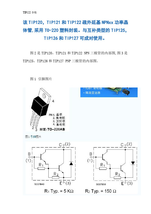
该TIP120,TIP121和TIP122疏外延基NPNxx功率晶体管,采用TO-220塑料封装。
与互补类型的TIP125,TIP126和TIP127可成对使用。
图2是TIP120,TIP121和TIP122 NPN三极管的内部图,图3是TIP125,TIP126和TIP127 PNP三极管的内部图。
图1 引脚图片xx电阻R1,R2起分流作用,使对温度敏感的穿透电流多了一个通路,就不会全部进入下一级的基极,同时xx电阻降低了发射结反向电阻,管子截止时发射极不易被反向电压击穿,但是电阻也增加了前级的负载。
xx管IC,一般都是用来驱动功率稍微大一点的被动器件的,而驱动的被动器件里,有很大一部分是感性的,如继电器、xx、等,这些感性器件在关断瞬间会产生很高的自感电动势(自感电压),低的10多伏,高的几十伏,甚至几百伏,这么高的电压很容易把xx管打坏,甚至打坏电路中的其它元器件,所以需要在感性器件上xx一个二极管,用来续流(就是把那个自感高压放掉),保护IC和其它器件不受破坏,此正极接2803输出端(即电感器件的一端),负极接驱动电源(也就是电感器件的另一端)。
在内部设计了二极管以后,用户在使用的时候不需要外接二极管,在同时驱动多路器件的时候可以节省PCB空间,节约成本、方便走线。
xx管就是两个三极管接在一起,极性只认前面的三极管。
具体接法如下,以两个相同极性的三极管为例,前面三极管跟后面三极管集电极相接,前面三极管发射极跟后面三极管基极相接,前面功率一般比后面三极管小,前面三极管基极为xx管基极,后面三极管发射极为xx管发射极,用法跟三极管一样,放大倍数是两个三极管放大倍数的乘积。
1复合管原理管xx管又称。
为共基组合,以组成一只等效的新的三极管。
这等效于三极管的放大倍数是二者之积。
在电路设计中,xx接法常用于功率放大器和稳压电xx管是一重复合三极管,他将两个三极管xx,第一个管子的发射极接第2个管子的基极,所以xx管的放大倍数是两个三极管放大倍数的乘积。
达林顿管型号及参数
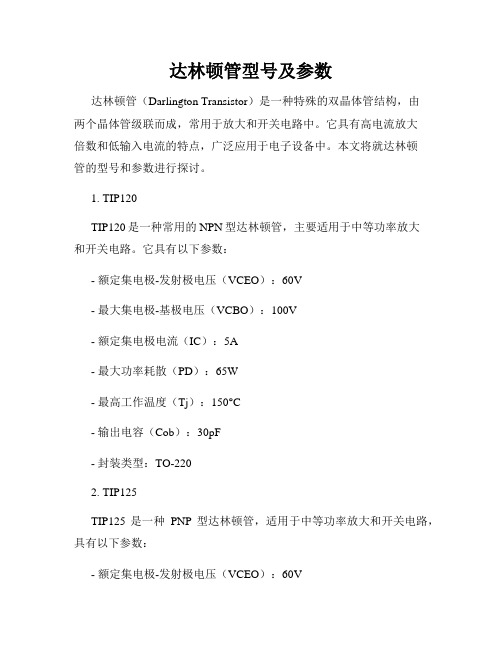
达林顿管型号及参数达林顿管(Darlington Transistor)是一种特殊的双晶体管结构,由两个晶体管级联而成,常用于放大和开关电路中。
它具有高电流放大倍数和低输入电流的特点,广泛应用于电子设备中。
本文将就达林顿管的型号和参数进行探讨。
1. TIP120TIP120是一种常用的NPN型达林顿管,主要适用于中等功率放大和开关电路。
它具有以下参数:- 额定集电极-发射极电压(VCEO):60V- 最大集电极-基极电压(VCBO):100V- 额定集电极电流(IC):5A- 最大功率耗散(PD):65W- 最高工作温度(Tj):150°C- 输出电容(Cob):30pF- 封装类型:TO-2202. TIP125TIP125是一种PNP型达林顿管,适用于中等功率放大和开关电路,具有以下参数:- 额定集电极-发射极电压(VCEO):60V- 最大集电极-基极电压(VCBO):60V- 额定集电极电流(IC):5A- 最大功率耗散(PD):65W- 最高工作温度(Tj):150°C- 输出电容(Cob):30pF- 封装类型:TO-2203. MPSA14MPSA14是一种通用型NPN型达林顿管,常用于低噪声放大和开关电路,具有以下参数:- 额定集电极-发射极电压(VCEO):30V- 最大集电极-基极电压(VCBO):40V- 额定集电极电流(IC):500mA- 最大功率耗散(PD):625mW- 最高工作温度(Tj):150°C- 输出电容(Cob):4.5pF- 封装类型:TO-924. MPSA13MPSA13是一种通用型PNP型达林顿管,适用于低噪声放大和开关电路,具有以下参数:- 额定集电极-发射极电压(VCEO):30V- 最大集电极-基极电压(VCBO):40V- 额定集电极电流(IC):500mA- 最大功率耗散(PD):625mW- 最高工作温度(Tj):150°C- 输出电容(Cob):4.5pF- 封装类型:TO-925. TIP122TIP122是一种高功率NPN型达林顿管,适用于高频放大和开关电路,常用于电机驱动等应用场合,具有以下参数:- 额定集电极-发射极电压(VCEO):100V- 最大集电极-基极电压(VCBO):100V- 额定集电极电流(IC):5A- 最大功率耗散(PD):65W- 最高工作温度(Tj):150°C- 输出电容(Cob):65pF- 封装类型:TO-220总结:以上介绍了几种常见的达林顿管型号及其参数,包括TIP120、TIP125、MPSA14、MPSA13和TIP122。
维希亚 Siliconix S12-1170-Rev. A 自动汽车N-通道 40V(D-S) 17
SQJ858AEP-T1-GE3SQJ858AEPVishay SiliconixAutomotive N-Channel 40 V (D-S) 175 °C MOSFETFEATURES•TrenchFET ® Power MOSFET •AEC-Q101 Qualified •100 % R g and UIS Tested•Material categorization:For definitions of compliance please see /doc?99912Notesa.Pulse test; pulse width ≤ 300 μs, duty cycle ≤ 2 %.b.When mounted on 1" square PCB (FR-4 material).c.Parametric verification ongoing.d.See solder profile (/doc?73257). The PowerPAK SO-8L is a leadless package. The end of the lead terminal is exposed copper (not plated) as a result of the singulation process in manufacturing. A solder fillet at the exposed copper tip cannot be guaranteed and is not required to ensure adequate bottom side solder interconnection.e.Rework conditions: manual soldering with a soldering iron is not recommended for leadless components.PRODUCT SUMMARYV DS (V)40R DS(on) (Ω) at V GS = 10 V 0.0063R DS(on) (Ω) at V GS = 4.5 V 0.0075I D (A)58ConfigurationSingleORDERING INFORMATIONPackagePowerPAK SO-8L Lead (Pb)-free and Halogen-freeSQJ858AEP-T1-GE3ABSOLUTE MAXIMUM RATINGS (T C = 25 °C, unless otherwise noted)PARAMETER S YMBOL LIMIT UNIT Drain-Source Voltage V DS40VGate-Source Voltage V GS ± 20Continuous Drain CurrentT C = 25 °C I D 58A T C = 125 °C33Continuous Source Current (Diode Conduction)I S 43Pulsed Drain Current aI DM 230Single Pulse Avalanche Current L = 0.1 mH I AS 35Single Pulse Avalanche Energy E AS 61mJ Maximum Power Dissipation aT C = 25 °C P D 48W T C = 125 °C 16Operating Junction and Storage Temperature Range T J , T stg- 55 to + 175°C Soldering Recommendations (Peak Temperature)d, e260THERMAL RESISTANCE RATINGSPARAMETER S YMBOL LIMIT UNIT Junction-to-Ambient PCB Mount bR thJA 85°C/WJunction-to-Case (Drain)R thJC3.1SQJ858AEPVishay SiliconixNotesa.Pulse test; pulse width ≤ 300 μs, duty cycle ≤ 2 %.b.Guaranteed by design, not subject to production testing.c.Independent of operating temperature.Stresses beyond those listed under “Absolute Maximum Ratings” may cause permanent damage to the device. These are stress ratings only, and functional operation of the device at these or any other conditions beyond those indicated in the operational sections of the specifications is not implied. Exposure to absolute maximum rating conditions for extended periods may affect device reliability.SPECIFICATIONS (T C = 25 °C, unless otherwise noted)PARAMETER S YMBOL TE S T CONDITION S MIN.TYP.MAX.UNITStaticDrain-Source Breakdown Voltage V DS V GS = 0, I D = 250 μA 40--V Gate-Source Threshold Voltage V GS(th)V DS = V GS , I D = 250 μA 1.5 2.0 2.5Gate-Source LeakageI GSS V DS = 0 V, V GS = ± 20 V--± 100nAZero Gate Voltage Drain Current I DSS V GS = 0 V V DS = 40 V --1μA V GS = 0 V V DS = 40 V, T J = 125 °C --50V GS = 0 V V DS = 40 V, T J = 175 °C--250On-State Drain Current aI D(on)V GS = 10 V V DS ≥ 5 V 30--A Drain-Source On-State Resistance aR DS(on)V GS = 10 VI D = 14 A -0.00500.0063ΩV GS = 4.5 V I D = 10 A -0.00600.0075V GS = 10 V I D = 14 A, T J = 125 °C --0.0120V GS = 10 VI D = 14 A, T J = 175 °C--0.0150Forward Transconductance b g fsV DS = 14 V, I D = 16 A-99-S Dynamic bInput Capacitance C issV GS = 0 V V DS = 20 V, f = 1 MHz -19512450pF Output CapacitanceC oss -295370Reverse Transfer Capacitance C rss -110140Total Gate Charge c Q gV GS = 10 V V DS = 20 V, I D = 20 A -3655nC Gate-Source Charge c Q gs -8-Gate-Drain Charge c Q gd -6-Gate Resistance R g f = 1 MHz1.52.97 4.5ΩTurn-On Delay Time c t d(on)V DD = 20 V, R L = 2 ΩI D ≅ 10 A, V GEN = 10 V, R g = 1 Ω-1015ns Rise Time ct r-914Turn-Off Delay Time c t d(off) -2640Fall Time c t f -812Source-Drain Diode Ratings and Characteristics bPulsed Current a I SM --230A Forward VoltageV SDI F = 15 A, V GS = 0-0.81.1VSQJ858AEP Vishay SiliconixTYPICAL CHARACTERISTICS (T A = 25 °C, unless otherwise noted)Output Characteristics TransconductanceCapacitanceTransfer CharacteristicsOn-Resistance vs. Drain CurrentGate ChargeSQJ858AEP Vishay SiliconixTYPICAL CHARACTERISTICS (T A = 25 °C, unless otherwise noted)Drain Source Breakdown vs. Junction TemperatureSQJ858AEP Vishay SiliconixTHERMAL RATINGS (T A = 25 °C, unless otherwise noted)Safe Operating AreaNormalized Thermal Transient Impedance, Junction-to-AmbientSQJ858AEP Vishay SiliconixTHERMAL RATINGS (T A = 25 °C, unless otherwise noted)Normalized Thermal Transient Impedance, Junction-to-CaseNote•The characteristics shown in the two graphs- Normalized Transient Thermal Impedance Junction-to-Ambient (25 °C)- Normalized Transient Thermal Impedance Junction-to-Case (25 °C)are given for general guidelines only to enable the user to get a “ball park” indication of part capabilities. The data are extracted from single pulse transient thermal impedance characteristics which are developed from empirical measurements. The latter is valid for the part mounted on printed circuit board - FR4, size 1" x 1" x 0.062", double sided with 2 oz. copper, 100 % on both sides. The part capabilities can widely vary depending on actual application parameters and operating conditions.Vishay Silicon ix main tain s worldwide man ufacturin g capability. Products may be man ufactured at on e of several qualified location s. Reliability data for Silicon Technology and Package Reliability represent a composite of all qualified locations. For related documents such as package/tape drawings, part marking, and reliability data, see /ppg?63470.Ordering Information Vishay SiliconixPowerPAK® SO-8LOrdering codes for the SQ rugged series power MOSFETs in the PowerPAK SO-8L package:DATASHEET PART NUMBER OLD ORDERING CODE a NEW ORDERING CODE SQJ200EP-SQJ200EP-T1_GE3SQJ202EP-SQJ202EP-T1_GE3SQJ401EP SQJ401EP-T1-GE3SQJ401EP-T1_GE3SQJ402EP SQJ402EP-T1-GE3SQJ402EP-T1_GE3SQJ403EEP SQJ403EEP-T1-GE3SQJ403EEP-T1_GE3SQJ403EP-SQJ403EP-T1_GE3SQJ410EP SQJ410EP-T1-GE3SQJ410EP-T1_GE3SQJ412EP SQJ412EP-T1-GE3SQJ412EP-T1_GE3SQJ422EP SQJ422EP-T1-GE3SQJ422EP-T1_GE3SQJ431EP SQJ431EP-T1-GE3SQJ431EP-T1_GE3SQJ443EP SQJ443EP-T1-GE3SQJ443EP-T1_GE3SQJ446EP-SQJ446EP-T1_GE3SQJ456EP SQJ456EP-T1-GE3SQJ456EP-T1_GE3SQJ459EP-SQJ459EP-T1_GE3SQJ460AEP-SQJ460AEP-T1_GE3SQJ461EP SQJ461EP-T1-GE3SQJ461EP-T1_GE3SQJ463EP SQJ463EP-T1-GE3SQJ463EP-T1_GE3SQJ465EP SQJ465EP-T1-GE3SQJ465EP-T1_GE3SQJ469EP SQJ469EP-T1-GE3SQJ469EP-T1_GE3SQJ486EP SQJ486EP-T1-GE3SQJ486EP-T1_GE3SQJ488EP SQJ488EP-T1-GE3SQJ488EP-T1_GE3SQJ500AEP SQJ500AEP-T1-GE3SQJ500AEP-T1_GE3SQJ840EP SQJ840EP-T1-GE3SQJ840EP-T1_GE3SQJ844AEP SQJ844AEP-T1-GE3SQJ844AEP-T1_GE3SQJ850EP SQJ850EP-T1-GE3SQJ850EP-T1_GE3SQJ858AEP SQJ858AEP-T1-GE3SQJ858AEP-T1_GE3SQJ886EP SQJ886EP-T1-GE3SQJ886EP-T1_GE3SQJ910AEP SQJ910AEP-T1-GE3SQJ910AEP-T1_GE3SQJ912AEP SQJ912AEP-T1-GE3SQJ912AEP-T1_GE3SQJ940EP SQJ940EP-T1-GE3SQJ940EP-T1_GE3SQJ942EP SQJ942EP-T1-GE3SQJ942EP-T1_GE3SQJ951EP SQJ951EP-T1-GE3SQJ951EP-T1_GE3SQJ952EP-SQJ952EP-T1_GE3SQJ956EP SQJ956EP-T1-GE3SQJ956EP-T1_GE3SQJ960EP SQJ960EP-T1-GE3SQJ960EP-T1_GE3SQJ963EP SQJ963EP-T1-GE3SQJ963EP-T1_GE3SQJ968EP SQJ968EP-T1-GE3SQJ968EP-T1_GE3SQJ980AEP SQJ980AEP-T1-GE3SQJ980AEP-T1_GE3SQJ992EP SQJ992EP-T1-GE3SQJ992EP-T1_GE3Notea.Old ordering code is obsolete and no longer valid for new ordersPackage Information Vishay SiliconixPowerPAK® SO-8L Case Outlinefor all PartsPackage InformationVishay SiliconixNote•Millimeters will goverLIMETERSINCHESMIN.NOM.MAX.MIN.NOM.MAX.A 1.00 1.07 1.140.0390.0420.045A10.00-0.1270.00-0.005b 0.330.410.480.0130.0160.019b10.440.510.580.0170.0200.023b2 4.804.905.000.1890.1930.197b30.0940.004b40.470.019c 0.200.250.300.0080.0100.012D 5.00 5.13 5.250.1970.2020.207D1 4.80 4.90 5.000.1890.1930.197D2 3.86 3.96 4.060.1520.1560.160D3 1.631.73 1.830.0640.0680.072e 1.27 BSC0.050 BSCE 6.05 6.15 6.250.2380.2420.246E1 4.27 4.37 4.470.1680.1720.176E2 2.75 2.85 2.950.1080.1120.116F --0.15--0.006L 0.620.720.820.0240.0280.032L10.921.07 1.220.0360.0420.048K 0.510.020W 0.230.009W10.410.016W2 2.820.111W3 2.960.117q0°-10°0°-10°ECN: C15-1203-Rev. A, 07-Sep-15DWG: 6044PAD PatternVishay SiliconixRevision: 07-Feb-121Document Number: 63818THIS DOCUMENT IS SUBJECT TO CHANGE WITHOUT NOTICE. THE PRODUCTS DESCRIBED HEREIN AND THIS DOCUMENTARE SUBJECT TO SPECIFIC DISCLAIMERS, SET FORTH AT /doc?91000RECOMMENDED MINIMUM PAD FOR PowerPAK ® SO-8L SINGLELegal Disclaimer Notice VishayDisclaimerALL PRODU CT, PRODU CT SPECIFICATIONS AND DATA ARE SU BJECT TO CHANGE WITHOU T NOTICE TO IMPROVE RELIABILITY, FUNCTION OR DESIGN OR OTHERWISE.Vishay Intertechnology, Inc., its affiliates, agents, and employees, and all persons acting on its or their behalf (collectively,“Vishay”), disclaim any and all liability for any errors, inaccuracies or incompleteness contained in any datasheet or in any other disclosure relating to any product.Vishay makes no warranty, representation or guarantee regarding the suitability of the products for any particular purpose or the continuing production of any product. To the maximum extent permitted by applicable law, Vishay disclaims (i) any and all liability arising out of the application or use of any product, (ii) any and all liability, including without limitation special, consequential or incidental damages, and (iii) any and all implied warranties, including warranties of fitness for particular purpose, non-infringement and merchantability.Statements regarding the suitability of products for certain types of applications are based on Vishay’s knowledge of typical requirements that are often placed on Vishay products in generic applications. Such statements are not binding statements about the suitability of products for a particular application. It is the customer’s responsibility to validate that a particular product with the properties described in the product specification is suitable for use in a particular application. Parameters provided in datasheets and/or specifications may vary in different applications and performance may vary over time. All operating parameters, including typical parameters, must be validated for each customer application by the customer’s technical experts. Product specifications do not expand or otherwise modify Vishay’s terms and conditions of purchase, including but not limited to the warranty expressed therein.Except as expressly indicated in writing, Vishay products are not designed for use in medical, life-saving, or life-sustaining applications or for any other application in which the failure of the Vishay product could result in personal injury or death. Customers using or selling Vishay products not expressly indicated for use in such applications do so at their own risk. Please contact authorized Vishay personnel to obtain written terms and conditions regarding products designed for such applications. No license, express or implied, by estoppel or otherwise, to any intellectual property rights is granted by this document or by any conduct of Vishay. Product names and markings noted herein may be trademarks of their respective owners.Material Category PolicyVishay Intertechnology, Inc. hereby certifies that all its products that are identified as RoHS-Compliant fulfill the definitions and restrictions defined under Directive 2011/65/EU of The European Parliament and of the Council of June 8, 2011 on the restriction of the use of certain hazardous substances in electrical and electronic equipment (EEE) - recast, unless otherwise specified as non-compliant.Please note that some Vishay documentation may still make reference to RoHS Directive 2002/95/EC. We confirm that all the products identified as being compliant to Directive 2002/95/EC conform to Directive 2011/65/EU.Vishay Intertechnology, Inc. hereby certifies that all its products that are identified as Halogen-Free follow Halogen-Free requirements as per JEDEC JS709A standards. Please note that some Vishay documentation may still make reference to the IEC 61249-2-21 definition. We confirm that all the products identified as being compliant to IEC 61249-2-21 conform to JEDEC JS709A standards.Revision: 02-Oct-121Document Number: 91000SQJ858AEP-T1-GE3。
TMP122中文资料
TMP122TMP124SBOS272B – JUNE 2003 – REVISED DECEMBER 2003DESCRIPTIONThe TMP122 and TMP124 are SPI-compatible temperature sensors available in SOT23-6 and SO-8 packages. Requir-ing only a pull-up resistor for complete function, the TMP122and TMP124 temperature sensors are capable of measuring temperatures within 2°C of accuracy over a temperature range of –40°C to +125°C, with operation up to 150°C.Programmable resolution, programmable set points and shut down function provide versatility for any application. Low supply current and a supply range from 2.7V to 5.5V make the TMP122 and TMP124 excellent candidates for low-power applications.The TMP122 and TMP124 are ideal for extended thermal measurement in a variety of communication, computer, con-sumer, environmental, industrial, and instrumentation appli-cations.FEATURESq DIGITAL OUTPUT: SPI-Compatible Interface q PROGRAMMABLE RESOLUTION:9- to 12-Bits + Sign q ACCURACY:±1.5°C from –25°C to +85°C (max)±2.0°C from –40°C to +125°C (max)q LOW QUIESCENT CURRENT: 50µA q WIDE SUPPLY RANGE: 2.7V to 5.5V q TINY SOT23-6 AND SO-8 PACKAGES q OPERATION TO 150°Cq PROGRAMMABLE HIGH/LOW SETPOINTSCopyright © 2003, Texas Instruments Incorporated1.5°C Accurate Programmable Digital Temperature Sensorswith SPI™ InterfacePlease be aware that an important notice concerning availability, standard warranty, and use in critical applications of Texas Instruments semiconductor products and disclaimers thereto appears at the end of this data sheet.APPLICATIONSq POWER-SUPPLY TEMPERATURE MONITORING q COMPUTER PERIPHERAL THERMAL PROTECTION q NOTEBOOK COMPUTERS q CELL PHONESq BATTERY MANAGEMENT q OFFICE MACHINESq THERMOSTAT CONTROLSq ENVIRONMENTAL MONITORING and HVACqELECTROMECHANICAL DEVICE TEMPERATURETMP122SO/ICSSCKSPI is a registered trademark of Motorola. All other trademarks are the property of their respective owners.V+CSNCALERTPRODUCTION DATA information is current as of publication date.Products conform to specifications per the terms of Texas Instruments standard warranty. Production processing does not necessarily include testing of all parameters.TMP122, TMP1242SBOS272BABSOLUTE MAXIMUM RATINGS (1)Power Supply, V+..................................................................................7V Input Voltage (2).......................................................................–0.3V to 7V Input Current.....................................................................................10mA Operating Temperature Range ......................................–55°C to +150°C Storage Temperature Range .........................................–60°C to +150°C Junction Temperature (T J Max)....................................................+150°C Lead Temperature (soldering).......................................................+300°C NOTES: (1) Stresses above those listed under “Absolute Maximum Ratings ”may cause permanent damage to the device. Exposure to absolute maximum conditions for extended periods may affect device reliability. (2) Input voltage rating applies to all TMP122 and TMP124 input voltages.ELECTROSTATICDISCHARGE SENSITIVITYThis integrated circuit can be damaged by ESD. Texas Instru-ments recommends that all integrated circuits be handled with appropriate precautions. Failure to observe proper handling and installation procedures can cause damage.ESD damage can range from subtle performance degradation to complete device failure. Precision integrated circuits may be more susceptible to damage because very small parametric changes could cause the device not to meet its published specifications.SPECIFIED PACKAGE TEMPERATUREPACKAGE ORDERING TRANSPORT PRODUCT PACKAGE-LEADDESIGNATOR (1)RANGE MARKING NUMBER MEDIA, QUANTITY TMP122SOT23-6DBV–40°C to +125°CT122TMP122AIDBVT Tape and Reel, 250"""""TMP122AIDBVR Tape and Reel, 3000TMP124SO-8D –40°C to +125°CT124TMP124AID Rails, 100"""""TMP124AIDRTape and Reel, 2500PACKAGE/ORDERING INFORMATIONNOTE: (1) For the most current specifications and package information, refer to our web site at .PIN CONFIGURATIONSTMP122, TMP1243SBOS272BPARAMETERCONDITIONMIN TYPMAX UNITS TEMPERATURE INPUT Range–40+125°C Accuracy (Temperature Error)–25°C to +85°C ±0.5±1.5°C –40°C to +125°C ±1.0±2.0°C –55°C to +150°C±1.5°C vs Supply –0.30.1+0.3°C/V Resolution (1)Selectable±0.0625°CDIGITAL INPUT/OUTPUT Input Logic Levels:V IH 0.7(V+)V V IL0.3(V+)V Input Current, SO/I, SCK, CS 0V ≤ V IN ≤ V+±1µA Output Logic Levels:V OL SO/I I SINK = 3mA 0.4V V OH SO/I I SOURCE = 2mA (V+)–0.4V V OL ALERTI SINK = 4mA 0.4V Leakage Current ALERT0V ≤ V IN ≤ 6V ±1µA Input Capacitance, SO/I, SCK, CS, ALERT 2.5pF ResolutionSelectable 9 to 12 + SignBits Conversion Time9-Bit + Sign 3040ms 10-Bit + Sign 6080ms 11-Bit + Sign 120160ms 12-Bit + Sign240320ms POWER SUPPLY Operating Range 2.75.5V Quiescent Current I Q Serial Bus Inactive 5075µA Shutdown Current I SDSerial Bus Inactive0.11µA TEMPERATURE RANGE Specified Range –40+125°C Operating Range –55+150°C Storage Range–60+150°C Thermal Resistance, θJASOT23-6 Surface-Mount 200°C/W SO-8 Surface-Mount150°C/WNOTE: (1) Specified for 12-bit resolution.ELECTRICAL CHARACTERISTICSAt T A = –40°C to +125°C, and V+ = 2.7V to 5.5V, unless otherwise noted.TMP122, TMP124TMP122, TMP1244SBOS272BTYPICAL CHARACTERISTICSAt T A = +25°C, and V+ = 5.0V, unless otherwise noted.7060504030QUIESCENT CURRENT vs TEMPERATURETemperature (°C)–60–40–2020406080100120140I Q (µA )1.00.90.80.70.60.50.40.30.20.10.0–0.1SHUTDOWN CURRENT vs TEMPERATURETemperature (°C)–60–40–2020406080100120140I S D (µA)400300200100CONVERSION TIME vs TEMPERATURETemperature (°C)–60–40–2020406080100120140C o n v e r s i o n T i m e (m s )2.01.51.00.50.0–0.5–1.0–1.5–2.0TEMPERATURE ACCURACY vs TEMPERATURETemperature (°C)–60–40–2020406080100120160140T e m p e r a t u r e E r r o r (°C)元器件交易网TMP122, TMP1245SBOS272BAPPLICATIONS INFORMATIONThe TMP122 and TMP124 digital temperature sensors are optimal for thermal management and thermal protection appli-cations. The TMP122/TMP124 are SPI interface-compatible and specified for a temperature range of –40°C to +125°C.The TMP122/TMP124 require minimal external components for operation, needing only a pull-up resistor on the ALERT pin and a bypass capacitor on the supply. Bypass capacitors of 0.1µF is recommended. Figure 1 shows typical connec-tions for the TMP122 and TMP124.FIGURE 1. Typical Connections of the TMP122 and MUNICATING WITH THE TMP122The TMP122/TMP124 converts continuously. If CS is brought low during a conversion the conversion process continues, but the last completed conversion is available at the output regis-ter. Communication with the TMP122/TMP124 is initiated by pulling CS low. The first 16 clocks of data transfer will return temperature data from the temperature sensors. The 16-bit data word is clocked out sign bit first, followed by the MSB. Any portion of the 16-bit word may be read before raising CS . If the user wishes to continue with CS low, the following 16 clocks transfer in a READ or WRITE command. READ and WRITE commands are described in Tables I and II.The READ command contains an embedded address in bits D4 and D3 to identify which register to read. Bits D4 and D3are internally registered and will hold their value following a READ command until a entire 16-bit read is completed by the user. The completion of the 16-bit READ acknowledges that the READ command has been completed. If the user issues a READ command and then raises CS with less than 16subsequent clocks, the data from that register will be available at the next fall of CS . The registered READ address will remain in effect until a full 16 clocks have been received. After the completion of a 16-bit READ from the part, the READ address is reset to return data from the Temperature Register.A WRITE command to a register will not change the READ address registered. For further discussion on the READ ad-dress register, see the Read Address Register section.Multiple commands may be strung together as illustrated in Figure 2. The TMP122/TMP124 accepts commands alternat-ing with 16-bit response data. On lowering CS , the part always responds with a READ from the address location indicated by the READ address register. If the next com-mand is a READ command then data is returned from the address specified by the READ command with the 16th clock resetting the READ address register to the default tempera-ture register. The TMP122/TMP124 then expect a 16-bit command. If the command is a WRITE command, then the 16 clocks following the command will again return tempera-ture data.Figures 3, 4, 5, and 6 detail the communication sequences.To maintain accuracy in applications requiring air or surface temperature measurement, care should be taken to isolate the package and leads from ambient air temperature.Read Command D15D14D13D12D11D10D9D8D7D6D5D4D3D2D1D0Temperature1000000000000000Configuration Register 1000000000001000Low Temp Threshold 1000000000010000High Temp Threshold111TABLE I. Read Command.Write Command D15D14D13D12D11D10D9D8D7D6D5D4D3D2D1D0Configuration Register 0000D1D0R1R0F1F0POL TM1TM0010Low Temp Threshold T12T11T10T9T8T7T6T5T4T3T2T1T0100High Temp Threshold T12T11T10T9T8T7T6T5T4T3T2T1T0110Shutdown Commandxxxxxxxx11111111TABLE II. Write Command.16-Bit READCSSO/I16-Bit READ COMMAND16-Bit Response16-Bit WRITE/Embedded Address16-Bit READFIGURE 2.Multiple Command Sequence.TMP122, TMP1246SBOS272BFIGURE 3. READ followed by WRITE COMMAND to T LOW /T HIGH Register.SO/ISCK SCK CS ZZ1D3D4D5D6D7D8D9D10D11D12D13D14D15SO/INOTE: (1) 0 indicates T LOW register, 1 indicates T HIGH register.CS 00/1(1)1T0T1T2T3T4T5T6T7T8T9T10T11T12SO/I16-Bit READ(Continued)...16-Bit WRITE/Embedded AddressCS...SO/ICS SCK SCK ZZ1D3D4D5D6D7D8D9D10D11D12D13D14D15SO/ICS 01TM0TM1POLF0F1R0R1D0D1SO/I16-Bit READ16-Bit WRITE/Embedded AddressCS...(Continued)...SO/ICS ZZ1D3D4D5D6D7D8D9D10D11D12D13D14D15SO/ICS ZZ 1D3D4D5D6D7D8D9D10D11D12D13D14D15SO/ICS 0P0P11SO/I16-Bit READ16-Bit READ COMMAND16-Bit ResponseCS ...(Continued)......(Continued)...SCK SCK SCK SO/ICS ZZ1D3D4D5D6D7D8D9D10D11D12D13D14D15SO/I16-Bit READCS SCK FIGURE 4. READ followed by WRITE COMMAND to Configuration Register.FIGURE 5. READ followed by READ COMMAND and Response.FIGURE 6. Data READ.TMP122, TMP1247SBOS272BREAD ADDRESS REGISTERFigure 7 shows the internal register structure of the TMP122/TMP124. Table III describes the addresses of the registers available. The READ address register uses the two bits to identify which of the data registers should respond to a read command. Following a complete 16-bit read, the READ address register is reset to the default power-up state of P1/P0 equal 0/0.The user can obtain 9, 10, 11, or 12 bits of resolution by addressing the Configuration Register and setting the reso-lution bits accordingly. For 9-, 10-, or 11-bit resolution, the most significant bits in the Temperature Register are used with the unused LSBs set to zero.CONFIGURATION REGISTERThe Configuration Register is a 16-bit read/write register used to store bits that control the operational modes of the temperature sensor. Read/write operations are performed MSB first. The format of the Configuration Register for the TMP122/TMP124 is shown in Table VI, followed by a break-down of the register bits. The power-up/reset value of the Configuration Register bits R1/R0 equal 1/1, all other bits equal zero.TEMPERATUREDIGITAL OUTPUT (1)(°C)(BINARY)HEX 150**** **** 0000 01114B071250011 1110 1000 01113E87250000 1100 1000 01110C870.06250000 0000 0000 1111000F 00000 0000 0000 01110007–0.06251111 1111 1111 1111FFFF –251111 0011 1000 0111F387–551110 0100 1000 0111E487NOTE: (1) The last 2 bits are high impedance and are shown as 11 in the table.TABLE V. Temperature Data Format.TEMPERATURE REGISTERThe Temperature Register of the TMP122/TMP124 is a 16-bit, signed read-only register that stores the output of the most recent conversion. The TMP122/TMP124 are speci-fied for the temperature range of –40°C to +125°C with operation from –55°C to +150°C. Up to 16 bits can be read to obtain data and are described in Table IV. The first 13 bits are used to indicate temperature where bit D2 is 1, and D1,D0 are in a high impedance state. Data format for tempera-ture is summarized in Table V. Following power-up or reset,the Temperature Register will read 0°C until the first conver-sion is complete.SHUTDOWN MODE (SD)The Shutdown Mode of the TMP122/TMP124 can be used to shut down all device circuitry except the serial interface.Shutdown mode occurs when the last 8 bits of the WRITE command are equal to 1, and will occur once the current conversion is completed, reducing current consumption to less than 1µA. To take the part out of shutdown, send any command or pattern after the 16-bit read with the last 8 bits not equal to one. Power on default is in active mode.TABLE III. Pointer Addresses of the TMP122 and TMP124Registers.D15D14D13D12D11D10D9D80000D1D0R1R0D7D6D5D4D3D2D1D0F1F0POLTM1TM01TABLE VI. Configuration Register.D15D14D13D12D11D10D9D8T12T11T10T9T8T7T6T5D7D6D5D4D3D2D1D0T4T3T2T1T01ZZTABLE IV. Temperature Register.TMP122, TMP1248SBOS272BF1F0CONSECUTIVE FAULTS001012104116TABLE VIII. Fault Settings of the TMP122 and TMP124.THERMOSTAT MODE (TM1/TM0)The Thermostat Mode bits of the TMP122/TMP124 indicate to the device whether to operate in Comparator Mode, Interrupt Mode or Interrupt Comparator Mode. For more information on Comparator and Interrupt Mode, see text HIGH and LOW limit registers. The bit assignments for thermostat mode are described in Table VII. Power on default is comparator mode.FAULT QUEUE (F1/F0)A fault condition occurs when the measured temperature exceeds the limits set in the T HIGH and T LOW registers. The Fault Queue is provided to prevent a false alert due to environmental noise and requires consecutive fault mea-surements to trigger the alert function of the TMP122/TMP124.Table VIII defines the number of consecutive faults required to trigger a consecutive alert condition. Power-on default for F1/F0 is 0/0.HIGH AND LOW LIMIT REGISTERSIn Comparator Mode (TM1/TM0 = 0/0), the ALERT Pin of the TMP122/TMP124 becomes active when the temperature equals or exceeds the value in T HIGH and generates a consecutive number of faults according to fault bits F1 and F0. The ALERT pin will remain active until the temperature falls below the indicated T LOW value for the same number of faults.In Interrupt Mode (TM1/TM0 = 0/1) the ALERT pin becomes active when the temperature equals or exceeds T HIGH for a consecutive number of fault conditions. The ALERT pin remains active until a read operation of any register occurs.The ALERT pin will also be cleared if the device is placed in Shutdown Mode. Once the ALERT pin is cleared, it will only become active again by the temperature falling below T LOW .When the temperature falls below T LOW , the ALERT pin becomes active and remains active until cleared by a read operation of any register. Once the ALERT pin is cleared, the above cycle will repeat with the ALERT pin becoming active when the temperature equals or exceeds T HIGH .In Interrupt/Comparator Mode (TM1/TM0 = 1/0), the ALERT Pin of the TMP122/TMP124 becomes active when the tem-perature equals or exceeds the value in T HIGH and generates a consecutive number of faults according to fault bits F1 and F0. The ALERT pin will remain active until the temperature falls below the indicated T LOW value for the same number of faults and a communication with the device has occurred after that point.Operational modes are represented in Figure 8. Tables IX and X describe the format for the T HIGH and T LOW registers.Power-up reset values for T HIGH and T LOW are: T HIGH = 80°C and T LOW = 75°C. The format of the data for T HIGH and T LOW is the same as for the Temperature Register.All 13 bits for the Temperature, T HIGH , and T LOW registers are used in the comparisons for the ALERT function for all con-verter resolutions. The three LSBs in T HIGH and T LOW can affect the ALERT output even if the converter is configured for 9-bit resolution.D15D14D13D12D11D10D9D8H12H11H10H9H8H7H6H5D7D6D5D4D3D2D1D0H4H3H2H1H011TABLE IX. T HIGH Register.D15D14D13D12D11D10D9D8L12L11L10L9L8L7L6L5D7D6D5D4D3D2D1D0L4L3L2L1L01TABLE X. T LOW Register.FIGURE 8. ALERT Output Transfer Function Diagrams.TMP122, TMP1249SBOS272BCONVERSION TIMER1R0RESOLUTION(typical)009 Bits (0.5°C) plus sign 30ms 0110 Bits (0.25°C) plus sign 60ms 1011 Bits (0.125°C) plus sign 120ms 1112 Bits (0.0625°C) plus sign240msTABLE XI. Resolution of the TMP122 and TMP124.CONVERTER RESOLUTION (R1/R0)The Converter Resolution Bits control the resolution of the internal Analog-to-Digital (A/D) converter. This allows the user to maximize efficiency by programming for higher resolution or faster conversion time. Table XI identifies the Resolution Bits and the relationship between resolution and conversion time.The TMP122/TMP124 have a default resolution of 12 bits.DELAY TIMEThe Delay Bits control the amount of time delay between each conversion. This feature allows the user to maximize power savings by eliminating unnecessary conversions, and minimiz-ing current consumption. During active conversion the TMP122/TMP124 typically requires 50µA of current for approximately 0.25s conversion time, and approximately 20µA for idle times between conversions. Delay settings are identified in Table XII as conversion time and period, and are shown in Figure 9.Default power up is D1/D0 equal 0/0. Conversion time and conversion periods scale with resolution. Conversion period denotes time between conversion starts.FIGURE 9. Conversion Time and Period Description.PARAMETER MIN MAX UNITS SCK Periodt 1100ns Data In to Rising Edge SCK Setup Time t 220nsSCK Falling Edge to Output Data Delay t 330ns SCK Rising Edge to Input Data Hold Time t 420ns CS to Rising Edge SCK Set-Up Time t 540ns CS to Output Data Delayt 630ns CS Rising Edge to Output High Impedancet 730nsTABLE XIII. Timing Description.Timing DiagramsThe TMP122/TMP124 are SPI compatible. Figures 10 to 12describe the various timing parameters of the TMP122/TMP124 with timing definitions in Table XIII.FIGURE 10. Output Data Timing Diagram.FIGURE 11. High Impedance Output Timing Diagram.FIGURE 12. Input Data Timing Diagram.TMP122, TMP124 10SBOS272BPACKAGING INFORMATIONOrderable Device Status (1)Package Type Package Drawing Pins Package Qty Eco Plan (2)Lead/Ball Finish MSL Peak Temp (3)TMP122AIDBVR ACTIVE SOT-23DBV 63000None CU NIPDAU Level-1-235C-UNLIM TMP122AIDBVT ACTIVE SOT-23DBV 6250None CU NIPDAU Level-1-235C-UNLIM TMP124AID ACTIVE SOIC D 8100Pb-Free (RoHS)CU NIPDAU Level-2-260C-1YEAR/Level-1-220C-UNLIM TMP124AIDRACTIVESOICD82500Pb-Free (RoHS)CU NIPDAULevel-2-260C-1YEAR/Level-1-220C-UNLIM(1)The marketing status values are defined as follows:ACTIVE:Product device recommended for new designs.LIFEBUY:TI has announced that the device will be discontinued,and a lifetime-buy period is in effect.NRND:Not recommended for new designs.Device is in production to support existing customers,but TI does not recommend using this part in a new design.PREVIEW:Device has been announced but is not in production.Samples may or may not be available.OBSOLETE:TI has discontinued the production of the device.(2)Eco Plan -May not be currently available -please check /productcontent for the latest availability information and additional product content details.None:Not yet available Lead (Pb-Free).Pb-Free (RoHS):TI's terms "Lead-Free"or "Pb-Free"mean semiconductor products that are compatible with the current RoHS requirements for all 6substances,including the requirement that lead not exceed 0.1%by weight in homogeneous materials.Where designed to be soldered at high temperatures,TI Pb-Free products are suitable for use in specified lead-free processes.Green (RoHS &no Sb/Br):TI defines "Green"to mean "Pb-Free"and in addition,uses package materials that do not contain halogens,including bromine (Br)or antimony (Sb)above 0.1%of total product weight.(3)MSL,Peak Temp.--The Moisture Sensitivity Level rating according to the JEDECindustry standard classifications,and peak solder temperature.Important Information and Disclaimer:The information provided on this page represents TI's knowledge and belief as of the date that it is provided.TI bases its knowledge and belief on information provided by third parties,and makes no representation or warrantyas to the accuracy of such information.Efforts are underway to better integrate information from third parties.TI has taken and continues to take reasonable steps to provide representative and accurate information but may not have conducted destructive testing or chemical analysis on incoming materials and chemicals.TI and TI suppliers consider certain information to be proprietary,and thus CAS numbers and other limited information may not be available for release.In no event shall TI's liability arising out of such information exceed the total purchase price of the TI part(s)at issue in this document sold by TI to Customer on an annual basis.PACKAGE OPTION ADDENDUM9-Dec-2004Addendum-Page 1IMPORTANT NOTICETexas Instruments Incorporated and its subsidiaries (TI) reserve the right to make corrections, modifications, enhancements, improvements, and other changes to its products and services at any time and to discontinue any product or service without notice. Customers should obtain the latest relevant information before placing orders and should verify that such information is current and complete. All products are sold subject to TI’s terms and conditions of sale supplied at the time of order acknowledgment.TI warrants performance of its hardware products to the specifications applicable at the time of sale in accordance with TI’s standard warranty. T esting and other quality control techniques are used to the extent TI deems necessary to support this warranty. Except where mandated by government requirements, testing of all parameters of each product is not necessarily performed.TI assumes no liability for applications assistance or customer product design. Customers are responsible for their products and applications using TI components. T o minimize the risks associated with customer products and applications, customers should provide adequate design and operating safeguards.TI does not warrant or represent that any license, either express or implied, is granted under any TI patent right, copyright, mask work right, or other TI intellectual property right relating to any combination, machine, or process in which TI products or services are used. Information published by TI regarding third-party products or services does not constitute a license from TI to use such products or services or a warranty or endorsement thereof. Use of such information may require a license from a third party under the patents or other intellectual property of the third party, or a license from TI under the patents or other intellectual property of TI.Reproduction of information in TI data books or data sheets is permissible only if reproduction is without alteration and is accompanied by all associated warranties, conditions, limitations, and notices. Reproduction of this information with alteration is an unfair and deceptive business practice. TI is not responsible or liable for such altered documentation.Resale of TI products or services with statements different from or beyond the parameters stated by TI for that product or service voids all express and any implied warranties for the associated TI product or service and is an unfair and deceptive business practice. TI is not responsible or liable for any such statements. Following are URLs where you can obtain information on other Texas Instruments products and application solutions:Products ApplicationsAmplifiers Audio /audioData Converters Automotive /automotiveDSP Broadband /broadbandInterface Digital Control /digitalcontrolLogic Military /militaryPower Mgmt Optical Networking /opticalnetwork Microcontrollers Security /securityTelephony /telephonyVideo & Imaging /videoWireless /wirelessMailing Address:Texas InstrumentsPost Office Box 655303 Dallas, Texas 75265Copyright 2004, Texas Instruments Incorporated。
tip122参数

tip122参数TIP122参数目录:1. 简介2. TIP122参数详解- 2.1 极限参数- 2.2 电气特性参数3. TIP122优势和应用4. 结论1. 简介TIP122是一种高电压以及高电流能力的开关型功率晶体管(BJT)。
它常用于各种功率应用电路中,特别是在高电流、高电压或需要能够控制大功率负载的情况下。
由于其可靠性和高性能,TIP122被广泛应用于工业、汽车、通信和电子设备等领域。
2. TIP122参数详解2.1 极限参数TIP122的极限参数决定了其在特定工作条件下的可靠性和性能。
以下是一些重要的极限参数:- VCEO:集电极-发射极最大电压。
它表示晶体管可以承受的最大反向电压,通常为100V之间,这使得它非常适合高电压应用。
- VCBO:集电极-基极最大电压。
这是集电极和基极之间的最大反向电压,通常也为100V左右。
- VEBO:发射极-基极最大电压。
它表示在基极与发射极之间的最大反向电压,通常约为10V。
- IC:集电极最大电流。
这是晶体管可以连续承受的最大电流,通常在5A-10A之间。
- IB:基极最大电流。
这是基极电流的最大允许值,通常约为2A-4A之间。
2.2 电气特性参数除了极限参数,许多其他电气特性参数也对TIP122的性能起着重要作用。
以下是一些关键的电气特性参数:- hFE:直流电流增益。
它描述了输入电流和输出电流之间的比例关系。
TIP122通常具有较高的hFE值,通常在1000以上。
- VCE(sat):饱和电压。
它是晶体管在开关状态下的最小集电极-发射极电压。
一般来说,这个值越低,晶体管的开关速度越快。
- Cob:输出电容。
它是晶体管集电极与基极之间的电容,这个值越小,晶体管的开关速度越快。
3. TIP122优势和应用TIP122之所以如此受欢迎并广泛应用,是因为它具有许多优势和适用性。
- 高电压和高电流承受能力:TIP122可以承受高达100V的电压和高达10A的电流,因此非常适合高功率负载或高电压应用。
新代参数设定参考手册

新代参数设定参考手册(总87页)-CAL-FENGHAI.-(YICAI)-Company One1-CAL-本页仅作为文档封面,使用请直接删除新代科技參數設定說明手冊by : 新代科技date :2006/11/20ver : 9.5版本更新記錄目錄1.參數總表 (7)2.參數設定說明 (36)2.1 系統基本參數設定 (36)2.1.1 硬體環境設定 (36)2.1.1.1 軸卡基本參數設定 (36)2.1.1.1.1Pr01 軸板基址 (36)2.1.1.1.2Pr09 軸板型態 (37)2.1.1.1.3 Pr10 伺服警報接點型態 (37)2.1.1.1.4Pr11 軸卡時脈來源 (38)2.1.1.1.5Pr12 SERVO6 軸卡最高時脈 (38)2.1.1.1.6Pr13 軸卡數目 (38)2.1.1.2 I/O 卡基本參數設定 (39)2.1.1.2.1Pr03 I/O 板基址 (39)2.1.1.2.2Pr05 I/O 板組態 (39)2.1.1.2.3Pr15 I/O 卡數位濾波程度 (42)2.1.1.3 控制精度設定 (43)2.1.1.3.1 Pr17 控制精度 (43)2.1.1.4 螢幕功能鍵型態設定 (43)2.1.1.4.1 Pr3205 功能鍵型態 (43)2.1.1.5 螢幕型別 (44)1 Pr3211 螢幕型別 (44)2.1.1.6 預設外部存取資料磁碟機代號 (44)1 Pr3213 磁碟機代號 (44)2.1.1.7 選擇控制面板鍵盤型態 (44)1 Pr3217 選擇控制面板鍵盤型別 (44)2.1.1.8 系統掃瞄時間設定 (45)1 Pr3202 I/O 掃描時間 (45)2 Pr3203 運動補間時間 (45)3 Pr3204 PLC 掃描時間 (45)2.1.2 軟體介面環境參數設定 (46)2.1.2.1 應用功能參數設定 (46)1 Pr411 G00 運動方式 (46)2 Pr413 G92(G92.1)座標保留模式設定 (46)2.1.2.1.3 Pr414 工件座標系統保留模式 (46)4 Pr415 重置或關機時保留目前刀長資料 (47)5 Pr3207 C/S 界面版本編號 (47)6 Pr3215 選刀時呼叫副程式 (47)7 Pr3241 工件程式小數點型態 (47)8 Pr3243 鍵盤重置鍵由 PLC 處理 (48)9 Pr3245 刀長磨耗補償輸入增量最大值 (48)0 Pr3801 G95 時進給量與主軸位置緊密偶合 (48)Pr3807 圓弧終點不在圓弧上檢查視窗 (49)2.1.2.1.12 Pr3809 UVW 為 XYZ 軸增量指令 (49)2.1.2.1.13 Pr3815 刀具半徑補償預看模式 (49)2.1.2.1.14 Pr3816 刀長補償模式 (49)5 Pr3819 過切檢查型態 (50)Pr3851 斷刀處理程式號碼 (50)2.1.2.2 系統人機介面設定 (51)1 Pr3201 設定啟動車床規則 (51)2 Pr3209 語言設定 (51)3 Pr3219 系統安裝組態 (52)4 Pr3221 除錯模式 (52)5 Pr3223 啟動系統管理功能 (53)6 Pr3225 螢幕保護功能延遲時間 (53)7 Pr3227 螢幕解析度 (53)2.1.2.2.8 Pr3229 關閉工件座標系統功能 (53)9 Pr3247 速率顯示方法 (54)2.2.伺服軸向參數設定 (55)2.2.1 各軸對應機械軸設定 (55)2.2.1.1 Pr21~Pr40 伺服對應的機械軸 (55)2.2.2 軸向馬達運動方向的設定 (55)2.2.2.1 Pr41~Pr60 馬達運動方向設定 (55)2.2.3 軸向命令與回授解析度設定 (56)2.2.3.1 Pr61~Pr80 位置感測器解析度 (56)Pr81~Pr100 軸卡回授倍頻 (56)Pr121~Pr160 螺桿側齒輪齒數,馬達側齒輪齒數 (56)Pr161~Pr180 螺桿寬度(Pitch) (56)Pr181~Pr200 伺服系統的位置迴路增益 (56)Pr201~Pr220 位置感測器型態 (56)Pr341~Pr360 位置命令倍率分子 (56)Pr361~Pr380 位置命令倍率分母 (56)2.2.4 各軸向應用型態設定 (58)2.2.4.1 Pr221~Pr226 軸型態 (58)2.2.4.2 Pr281~Pr300 選擇半徑軸或直徑軸 (59)2.2.5 各軸向顯示名稱設定 (59)2.2.5.1 P r321~Pr340 設定軸的名稱 (59)2.2.6 軸向控制模式設定 (60)2.2.6.1 Pr381~Pr400 位置伺服控制模式 (60)2.2.7 定位檢查功能設定 (60)2.2.7.1 Pr421~Pr440 切削時位置檢查的視窗範圍 (60)2.2.7.2 Pr481~Pr500 快速移動(Rapid T ravel, G00)時位置檢查的視窗範圍 (61)2.2.7.3 Pr561~Pr580 遺失位置檢查視窗 (61)2.2.7.4 Pr901~Pr920 零速檢查視窗 (61)2.2.8 各軸向左右軟體行程極限保護 (61)2.2.8.1 Pr2401~Pr2440 軟體第一行程保護的範圍 (61)2.2.8.2 Pr2441~Pr2480 軟體第二行程保護的範圍 (62)2.3.主軸參數設定 (63)2.3.1 主軸對應命令輸出埠設定 (63)2.3.1.1 Pr1621~Pr1630 主軸對應的機械軸或邏輯軸 (63)2.3.2 主軸命令參數設定 (63)2.3.2.1 Pr.1631~Pr.1636 主軸零速offset 速度 (63)2.3.2.2 Pr.1641~Pr.1646 主軸編碼器極性 (63)2.3.2.3 Pr.1651~Pr.1656 主軸馬達編碼器一轉的Pulse 數 (63)2.3.2.4 Pr.1661~Pr.1666 主軸回授倍頻 (64)2.3.2.5 Pr.1671~Pr.1676 主軸馬達增益 (64)2.3.2.6 Pr.1681~Pr.1692 主軸第一檔齒數比 (64)Pr.1901~Pr.1952 主軸第四檔齒數比 (64)2.3.2.7 P r.1711~Pr.1716 主軸是否安裝編碼器 (65)2.3.3 主軸運動轉速設定參數 (65)2.3.3.1 Pr.1721~Pr.1726 主軸寸動速度 (65)2.3.3.2 Pr.1731~Pr.1736 主軸最低轉速 (65)2.3.3.3 Pr.1801~Pr.1806 主軸最高轉速 (65)2.3.3.4 Pr.1821~Pr.1826 主軸伺服微分增益 (65)2.3.3.5 Pr.1831~Pr.1836 主軸加減速時間 (66)2.3.3.6 Pr.1851~Pr.1856 主軸重力加速度加減速時間 (66)2.3.4 主軸定位設定參數 (66)2.3.4.1 Pr.1741~Pr.1746 主軸定位速度 (66)2.3.4.2 Pr.1741~Pr.1746 主軸定位偏移量 (66)2.3.4.3 Pr.1771~Pr.1776 主軸原點偏移量 (66)2.3.4.4 Pr.1781~Pr.1786 主軸定位最低速度 (67)2.3.4.5 Pr.1791~Pr.1796 主軸馬達型態 (67)2.3.4.6 P r.1811~Pr.1816 主軸編碼器安裝位置 (67)2.3.4.7 Pr.1841~Pr.1846 主軸Y-Delta 切換速度 (67)2.4.軸向運動特性設定參數 (69)2.4.1 切削時前加減速運動規劃 (69)2.4.1.1 Pr401 切削加減速時間 (69)Pr402 重力加速度加減速時間 (69)Pr405 切削的最高進給速度 (69)Pr541~Pr560 各軸切削的加減速時間 (69)Pr621~Pr640 各軸切削的最高進給速度 (69)Pr641~Pr660 各軸重力加速度加減速時間 (69)2.4.2 切削時後加減速運動規劃 (71)2.4.2.1 Pr404 後加減速切削鐘型加減速時間 (71)2.4.3 切削時直線轉角自動減速功能 (73)2.4.3.1 P r406 轉角參考速度 (73)2.4.4 切削時圓弧切削運動最高進給速度設定 (74)2.4.4.1 Pr408 半徑5mm 圓弧切削參考速度 (74)2.4.5 快速移動及 JOG 時的加減速規劃 (75)2.4.5.1 Pr441~Pr460 各軸快速移動(G00)的加減速時間 (75)Pr461~Pr480 各軸快速移動(G00)的最高進給速度 (75)Pr501~Pr520 各軸快速移動(G00)的F0 速度 (75)Pr521~Pr540 各軸JOG 速度 (75)2.5.尋原點動作設定參數 (76)2.5.1 尋原點方式設定參數 (76)2.5.1.1 Pr961~Pr980 各軸尋原點方法 (76)2.5.2 尋原點動作規格與參數設定 (76)2.5.2.1 Pr821~Pr840 各軸第一段尋原點速度 (76)Pr841~Pr860 各軸第二段尋原點速度 (76)Pr861~Pr880 各軸尋原點為負方向 (76)2.5.3 原點偏移功能設定參數 (77)2.5.3.1 Pr881~Pr900 原點的偏移量設定 (77)2.5.4 原點柵格量功能設定參數 (78)2.5.4.1 Pr941~Pr960 啟動尋原點柵格功能 (78)2.6.手輪功能設定參數 (80)2.6.1 手輪訊號輸入設定參數 (80)2.6.1.1 Pr2031~Pr2034 手輪對應的機械軸 (80)2.6.2 手輪訊號解析度設定參數 (80)2.6.2.1 Pr2041~Pr2044 手輪Encoder 一轉的Pulse 數 (80)Pr2051~Pr2054 手輪回授倍頻 (80)2.6.3 手輪段數設定參數 (80)2.6.3.1 Pr2001 手輪第四段倍率設定 (80)2.6.4 手輪模擬功能設定參數 (81)2.6.4.1 Pr2003 手輪模擬對應手輪號碼 (81)2.6.5 手輪驅動軸向功能設定參數 (81)2.6.5.1 Pr2031~Pr2033 手輪對應的座標軸 (81)2.6.5 手輪設定參數 (81)2.6.5.1 Pr2031~Pr2033 手輪對應的座標軸 (81)2.7.機構補償功能設定參數 (82)2.7.1 尖角誤差補償設定參數 (82)2.7.1.1 Pr1361~Pr1380 圓弧尖角正向誤差補償量 (82)Pr1381~Pr1400 圓弧尖角誤差補償時間常數 (82)Pr1361~Pr1400 圓弧尖角負向誤差補償量 (82)2.8.軸耦合功能設定參數 (85)2.8.1 軸耦合功能設定參數 (85)2.8.1.1 Pr1361~Pr1380 圓弧尖角正向誤差補償量 (85)Pr1381~Pr1400 圓弧尖角誤差補償時間常數 (85)Pr1361~Pr1400 圓弧尖角負向誤差補償量 (85)1.參數總表2.參數設定說明2.1 系統基本參數設定2.1.1 硬體環境設定軸卡基本參數設定2.1.1.1.1 Pr01 軸板基址1.Servo_4 軸卡對應 I/O 基址與跳線規則:軸卡二片以下 Pr01今800 軸卡超過二片 Pr01今7682.S ervo_6 的第一片軸卡基址為768(目前一部控制器僅支援一張 Servo_6,不可與 Servo_4 混插)3.E mbedded 第一片軸卡基址固定為5122.1.1.1.2 Pr09 軸板型態0:EMP21:SVO4+不檢查伺服警報2:SVO4+伺服警報接點為常開接點 Normal Open( A 接點)3:SVO4+伺服警報接點為常閉接點 Normal Close( B 接點)4:EMP45:SERVO69:虛擬軸卡2.1.1.1.3 Pr10 伺服警報接點型態0: SERVO 6 軸卡警報為常開接點 Normal Open( A 接點)1: SERVO 6 軸卡警報為常閉接點 Normal Close( B 接點)2.1.1.1.4 Pr11 軸卡時脈來源此參數為設定軸卡時脈來源:設定 0 為使用軸卡自已時脈設定 1 為共用控制器底板 IPC Bus 時脈設定 2 為共用主機板 VIA 時脈設定原則:一體機控制器今請設定『0』非一體機控制器今請設定『2』舊型 486 主機板控制器今請設定『1』2.1.1.1.5 Pr12 SERVO6 軸卡最高時脈此參數為設定 Servo6 軸版最高時脈。
简易数控直流电压源报告
题目: 串联型直流稳压电源设计专业电子信息工程班级 09电信一班学号 090507128姓名黄志诚指导老师郭海燕摘要直流稳压电源一般由电源变压器,整流滤波电路及稳压电路组成。
变压器把高交流电变为需要的低压交流电。
整流器把交流电变为直流电。
经滤波后,稳压器再把不稳定的直流电压变为稳定的直流电压输出。
本次设计主要采用串联型直流稳压电路,通过220V 、50HZ交流电压经电源变压器降压后,通过桥式整流VD1—VD4整流成直流电再经过滤波电容平滑直流电,减少直流电纹波系数。
最后,通过稳压器稳压,将输出电压稳定在5V。
关键词:整流、滤波、电压源、过流保护2目录1 系统设计 (3)1.1设计要求 (3)1.1.1 设计任务................................... 错误!未定义书签。
1.1.2、基本要求 (4)1.1.3、发挥部分 (4)1.1.4 测试要求................................... 错误!未定义书签。
1.1.5 系统框图................................... 错误!未定义书签。
1.2方案论证与比较 (4)1.2.1电压采样模块 (10)1.2.2 稳压模块 (10)1.2.3 过载保护模块 (11)1.2.4 最终方案 (6)2.单元电路分析 (6)2.1D/A转换模块 (6)2.1.1工作原理 (6)2.1.2 参数选择 (7)2.2电压放大模块 (7)2.2.1 工作原理 (7)2.2.2 参数选择 (7)2.3稳定电压源及电压采样模块 (8)2.3.1 工作原理 (8)2.3.2 参数选择 (8)2.4过载保护模块 (9)2.4.1工作原理 (9)2.4.2 参数选择 (9)3.软件设计 (15)3.1实现功能....................................... 错误!未定义书签。
- 1、下载文档前请自行甄别文档内容的完整性,平台不提供额外的编辑、内容补充、找答案等附加服务。
- 2、"仅部分预览"的文档,不可在线预览部分如存在完整性等问题,可反馈申请退款(可完整预览的文档不适用该条件!)。
- 3、如文档侵犯您的权益,请联系客服反馈,我们会尽快为您处理(人工客服工作时间:9:00-18:30)。
该TIP120,TIP121和TIP122疏外延基NPN达林顿功率晶体管,采用TO-220塑料封装。
与互补类型的TIP125,TIP126和TIP127可成对使用。
图2是TIP120,TIP121和TIP122 NPN三极管的内部图,图3是TIP125,TIP126和TIP127 PNP三极管的内部图。
图1 引脚图片
并联电阻R1,R2起分流作用,使对温度敏感的穿透电流多了一个通路,就不会全部进入下一级的基极,同时并联电阻降低了发射结反向电阻,管子截止时发射极不易被反向电压击穿,但是电阻也增加了前级的负载。
达林顿管IC,一般都是用来驱动功率稍微大一点的被动器件的,而驱动的被动器件里,有很大一部分是感性的,如继电器、马达、电磁阀等,这些感性器件在关断瞬间会产生很高的自感电动势(自感电压),低的10多伏,高的几十伏,甚至几百伏,这么高的电压很容易把达林顿管打坏,甚至打坏电路中的其它元器件,所以需要在感性器件上并联一个二极管,用来续流(就是把那个自感高压放掉),保护IC和其它器件不受破坏,此续流二极管正极接
2803输出端(即电感器件的一端),负极接驱动电源(也就是电感器件的另一端)。
在内部设计了二极管以后,用户在使用的时候不需要外接二极管,在同时驱动多路器件的时候可以节省PCB空间,节约成本、方便走线。
达林顿管就是两个三极管接在一起,极性只认前面的三极管。
具体接法如下,以两个相同极性的三极管为例,前面三极管集电极跟后面三极管集电极相接,前面三极管发射极跟后面三极管基极相接,前面三极管功率一般比后面三极管小,前面三极管基极为达林顿管基极,后面三极管发射极为达林顿管发射极,用法跟三极管一样,放大倍数是两个三极管放大倍数的乘积。
1复合管原理
达林顿管原理
达林顿管又称复合管。
为共基组合放大器,以组成一只等效的新的三极管。
这等效于三极管的放大倍数是二者之积。
在电子学电路设计中,达林顿接法常用于功率放大器和稳压电林顿管是一重复合三极管,他将两个三极管串联,第一个管子的发射极接第2个管子的基极,所以达林顿管的放大倍数是两个三极管放大倍数的乘积。
所以它的特点是放大倍数非常高,达林顿管的作用一般是在高灵敏的放大电路中放大非常微小的信号。
如大功率开关电路。
2相关介绍编辑
达林顿电路有四种接法:NPN+NPN,PNP+PNP,NPN+PNP,PNP+NPN
前二种是同极性接法,后二种是异极性接法。
NPN+NPN的同极性接法:B1为B,C1C2为
C,E1B2接在一起,那么E2为E。
这里也说一下异极性接法。
以NPN+PNP为例。
设前一三极管T1的三极为C1B1E1,后一三极管T2的三极为C2B2E2。
达林顿管的接法应为:C1B2应接一起,E1C2应接一起。
等效三极管CBE的管脚,C=E2,B=B1,E=E1(即C2)。
等效三极管极性,与前一三极管相同。
即为NPN型。
PNP+NPN的接法与此类同。
NPN PNP
同极型达林顿三极管
NPN PNP 等效一只三极管
异极型达林顿三极管
达林顿管的典型应用
1、用于大功率开关电路、电机调速、逆变电路。
2、驱动小型继电器
利用CMOS电路经过达林顿管驱动高灵敏度继电器的电路,如右上图所示。
虚线框内是小功率NPN达林顿管FN020。
3、驱动LED智能显示屏
LED智能显示屏是由微型计算机控制,以LED矩阵板作显示的系统,可用来显示各种文字及图案。
该系统中的行驱动器和列驱动器均可采用高β、高速低压降的达林顿管。
图2是用BD683(或BD677)型中功率NPN达林顿管作为列驱动器,而用BD682(或BD678)型PNP达林顿管作行驱动器,控制8×8LED矩阵板上相应的行(或列)的像素发光。
应注意的是,达林顿管由于内部由多只管子及电阻组成,用万用表测试时,be结的正反向阻值与普通三极管不同。
对于高速达林顿管,有些管子的前级be结还反并联一只输入二极管,这时测出be结正反向电阻阻值很接近,容易误判断为坏管,请注意。
4、判断达林顿管等效为何种类型的三极管:
首先看看第一只管是什么类型的,第一只管是什么类型的,那么这只达林顿管就是什么类型的,与第二只无关!更加重要的是,要判断两个晶体管能否形成达林顿管关键要看电流,如果工作电流冲突,则不能构成达林顿管结构。
也可以根据PNP或者NPN管的标志来判断,其实本质上三极管上所标的箭头也是其工作电流的流向。