BAT54C中文资料
BAT54CLT1G;BAT54CLT3G;中文规格书,Datasheet资料
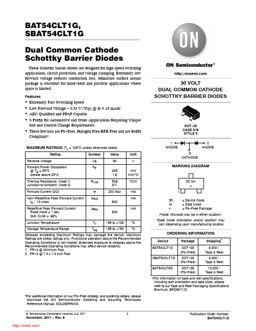
BAT54CLT1G,SBAT54CLT1GDual Common Cathode Schottky Barrier DiodesThese Schottky barrier diodes are designed for high speed switching applications, circuit protection, and voltage clamping. Extremely low forward voltage reduces conduction loss. Miniature surface mount package is excellent for hand−held and portable applications where space is limited.Features∙Extremely Fast Switching Speed∙Low Forward V oltage − 0.35 V (Typ) @ I F = 10 mAdc∙AEC Qualified and PPAP Capable∙S Prefix for Automotive and Other Applications Requiring Unique Site and Control Change Requirements∙These Devices are Pb−Free, Halogen Free/BFR Free and are RoHS Compliant*MAXIMUM RATINGS(T J = 125︒C unless otherwise noted)Rating Symbol Value Unit Reverse Voltage V R30VForward Power Dissipation @ T A = 25︒CDerate above 25︒C P F2251.8mWmW/︒CThermal Resistance (Note 1) Junction-to-Ambient (Note 2)R q JA508311︒C/WForward Current (DC)I F200 Max mANon−Repetitive Peak Forward Current t p < 10 msec I FSM600mARepetitive Peak Forward Current Pulse Wave = 1 sec,Duty Cycle = 66%IFRM300mAJunction Temperature T J−55 to +125︒C Storage Temperature Range T stg−55 to +150︒C Stresses exceeding Maximum Ratings may damage the device. Maximum Ratings are stress ratings only. Functional operation above the Recommended Operating Conditions is not implied. Extended exposure to stresses above the Recommended Operating Conditions may affect device reliability.1.FR−4 @ Minimum Pad.2.FR−4 @ 1.0 x 1.0 inch Pad.*For additional information on our Pb−Free strategy and soldering details, please download the ON Semiconductor Soldering and Mounting Techniques Reference Manual, SOLDERRM/D.30 VOLTDUAL COMMON CATHODE SCHOTTKY BARRIER DIODESCATHODE12MARKING DIAGRAM†For information on tape and reel specifications, including part orientation and tape sizes, please refer to our T ape and Reel Packaging Specifications Brochure, BRD8011/D.SOT−23CASE 318STYLE 95C= Device CodeM= Date CodeG= Pb−Free Package15C M GG*Date Code orientation and/or position mayvary depending upon manufacturing location.Device Package Shipping†ORDERING INFORMATIONBAT54CLT1G SOT−23(Pb−Free)3,000 /Tape & ReelBAT54CLT3G SOT−23(Pb−Free)10,000 /Tape & Reel (*Note: Microdot may be in either location) SBAT54CLT1G SOT−23(Pb−Free)3,000 /Tape & ReelELECTRICAL CHARACTERISTICS (T A = 25 C unless otherwise noted) (EACH DIODE)Characteristic Symbol Min Typ Max UnitReverse Breakdown Voltage (I R = 10 m A)V(BR)R30−−VTotal Capacitance(V R = 1.0 V, f = 1.0 MHz)C T−7.610pFReverse Leakage (V R = 25 V)I R−0.5 2.0m AForward Voltage (I F = 0.1 mAdc)V F−0.220.24VForward Voltage(I F = 30 mAdc)V F−0.410.5VForward Voltage(I F = 100 mAdc)V F−0.520.8VReverse Recovery Time(IF = I R = 10 mAdc, I R(REC) = 1.0 mAdc, Figure 1)trr−− 5.0nsForward Voltage(I F = 1.0 mAdc)V F−0.290.32VForward Voltage(I F = 10 mAdc)V F−0.350.40VNotes: 1. A 2.0 k W variable resistor adjusted for a Forward Current (I F) of 10 mA.2. Input pulse is adjusted so I R(peak) is equal to 10 mA.3. t p » t rrV Rt r10%90%IIOUTPUT PULSE(I F = I R = 10 mA; measuredat i R(REC) = 1 mA)INPUT SIGNALFigure 1. Recovery Time Equivalent Test CircuitC T , T O T A L C A P A C I T A N C E (p F )100V F , FORWARD VOLTAGE (VOLTS)101.00.110V R , REVERSE VOLTAGE (VOLTS)1.00.10.010.001140V R , REVERSE VOLTAGE (VOLTS)124205101530Figure 2. Forward VoltageFigure 3. Leakage CurrentFigure 4. Total Capacitance100100025206810I R , R E V E R S E C U R R E N T (m A )I F , F O R W A R D C U R R E N T (m A )PACKAGE DIMENSIONSSOT −23 (TO −236)CASE 318−08ISSUE APSTYLE 9:PIN 1.ANODE2.ANODE3.CATHODE*For additional information on our Pb −Free strategy and solderingdetails, please download the ON Semiconductor Soldering and Mounting Techniques Reference Manual, SOLDERRM/D.SOLDERING FOOTPRINT*NOTES:1.DIMENSIONING AND TOLERANCING PER ANSI Y14.5M, 1982.2.CONTROLLING DIMENSION: INCH.3.MAXIMUM LEAD THICKNESS INCLUDES LEAD FINISHTHICKNESS. MINIMUM LEAD THICKNESS IS THE MINIMUM THICKNESS OF BASE MATERIAL.4.DIMENSIONS D AND E DO NOT INCLUDE MOLD FLASH,PROTRUSIONS, OR GATE BURRS.VIEW CDIM A MIN NOM MAX MINMILLIMETERS0.89 1.00 1.110.035INCHES A10.010.060.100.001b 0.370.440.500.015c 0.090.130.180.003D 2.80 2.90 3.040.110E 1.20 1.30 1.400.047e 1.78 1.90 2.040.070L 0.100.200.300.0040.0400.0440.0020.0040.0180.0200.0050.0070.1140.1200.0510.0550.0750.0810.0080.012NOM MAX L1 2.10 2.40 2.640.0830.0940.104H E 0.350.540.690.0140.0210.0290−−−100−−−10q︒︒︒︒ON Semiconductor and are registered trademarks of Semiconductor Components Industries, LLC (SCILLC). SCILLC reserves the right to make changes without further notice to any products herein. SCILLC makes no warranty, representation or guarantee regarding the suitability of its products for any particular purpose, nor does SCILLC assume any liability arising out of the application or use of any product or circuit, and specifically disclaims any and all liability, including without limitation special, consequential or incidental damages.“Typical” parameters which may be provided in SCILLC data sheets and/or specifications can and do vary in different applications and actual performance may vary over time. All operating parameters, including “Typicals” must be validated for each customer application by customer’s technical experts. SCILLC does not convey any license under its patent rights nor the rights of others. SCILLC products are not designed, intended, or authorized for use as components in systems intended for surgical implant into the body, or other applications intended to support or sustain life, or for any other application in which the failure of the SCILLC product could create a situation where personal injury or death may occur. Should Buyer purchase or use SCILLC products for any such unintended or unauthorized application, Buyer shall indemnify and hold SCILLC and its officers, employees, subsidiaries, affiliates,and distributors harmless against all claims, costs, damages, and expenses, and reasonable attorney fees arising out of, directly or indirectly, any claim of personal injury or death associated with such unintended or unauthorized use, even if such claim alleges that SCILLC was negligent regarding the design or manufacture of the part. SCILLC is an Equal Opportunity/Affirmative Action Employer. This literature is subject to all applicable copyright laws and is not for resale in any manner.PUBLICATION ORDERING INFORMATION分销商库存信息:ONSEMIBAT54CLT1G BAT54CLT3G。
BAT54AL-AE3-R中文资料

UNISONIC TECHNOLOGIES CO., LTDBAT54x DIODESCHOTTKY BARRIER (DUAL) DIODESDESCRIPTIONPlanar Schottky barrier diodes encapsulated in the SOT-23 and SOT-323 small plastic SMD package. Single diodes and dual diodes with different pin configuration are available.FEATURES* Low forward voltage * Guard ring protected* Small plastic SMD package*Pb-free plating product number: BAT54xLORDERING INFORMATIONOrder Number Pin AssignmentNormal Lead Free Plating Package 1 2 3PackingBAT54-AE3-R BAT54L-AE3-R SOT-23 x A K Tape Reel BAT54A-AE3-R BAT54AL-AE3-R SOT-23 K1 K2 A2A1Tape Reel BAT54C-AE3-R BAT54CL-AE3-R SOT-23 A1 A2 K2K1Tape Reel BAT54S-AE3-R BAT54SL-AE3-R SOT-23 K1 A2 K2A1Tape Reel BAT54-AL3-R BAT54L-AL3-R SOT-323x A K Tape Reel BAT54A-AL3-R BAT54AL-AL3-R SOT-323K1 K2 A2A1Tape Reel BAT54C-AL3-R BAT54CL-AL3-R SOT-323A1 A2 K2K1Tape Reel BAT54S-AL3-R BAT54SL-AL3-R SOT-323K1 A2 K2A1Tape ReelDIODE CONFIGURATION AND SYMBOLMARKINGABSOLUTE MAXIMUM RATINGSPARAMETER SYMBOLRATINGS UNITPer diodeContinuous Reverse Voltage V R 30 V Continuous Forward Current I F 200 mA Repetitive Peak Forward Current (t p < 1s, δ ≤ 0.5) I FRM 300 mA Non-repetitive Peak Forward Current (t p < 10ms) I FSM 600 mA Junction Temperature T J +125 Storage Temperature T STG -60 ~ +150 Per devicePower Dissipation (T a ≤ 25 ) P D 230 mW Note Absolute maximum ratings are those values beyond which the device could be permanently damaged.Absolute maximum ratings are stress ratings only and functional device operation is not implied.THERMAL DATAPARAMETER SYMBOL RATINGS UNITSOT-23 500 K/WThermal Resistance From Junction to AmbientSOT-323JA 625 K/W ELECTRICAL CHARACTERISTICS (T a = 25 , unless otherwise specified.)PARAMETER SYMBOLTEST CONDITIONS MIN TYP MAX UNITForward Voltage (See Fig.1)V FI F = 0.1mAI F = 1mAI F = 10mA I F = 30mAI F = 100mA240320400500800mV mV mV mV mV Reverse Current (See Fig.2) I R V R = 25V 2 µA Reverse Recovery Time (see Fig.4) t rr When switched from I F =10mA to I R = 10mA, R L = 100Ω measured at I R = 1mA 5 ns Diode Capacitance (see Fig.3)C df = 1 MHz, V R = 1V; 10pFTYPICAL CHARACTERISTICS101000.40.8V F (V)I F (m A )101.2Fig.1 Forward current as a function of forward voltage ;typical values.101001020V R (V)I R ( A )1030Fig.2 Reverse current as a function of reverse voltage;typical values.10001020V R (V)C d (p F )30Fig.3 Diode capacitance as a function of reverse voltage;typical values.I I Fig.4 Reverse recovery definitions。
BAT54S BAT54肖特基二极管参数
℃
TJ
Operating Junction Temperature工作结温
-55 to +150
℃
电气特性:
符号
Parameter参数
Conditions测试条件
最小
最大
单位
VR
Breakdown Voltage击穿电压
IR30-Fra bibliotekVVF
Forward Voltage正向电压
IF = 0.1mA
IF = IR = 10mA, IRR = 1.0mA,
RL = 100Ω
-
5.0
nS
BAT54封装外型及引脚图
BAT54
BAT54A
BAT54C
BAT54S
BAT54FILM
BAT54AFILM
BAT54CFILM
BAT54SFILM
BAT54S BAT54肖特基二极管参数
来源:|时间:2010年05月02日
三端贴片肖特基二极管BAT54/BAT54A/BAT54C/BAT54S
特点:
极小传导损耗
开关损耗可以忽略不计
低正向压降
表面贴装器件
肖特基势垒二极管封装采用SOT-23
绝对最大额定值:
Symbol符号
Parameter参数
Value数值
Unit单位
VRRM
Maximum Repetitive Reverse Voltage最大重复反向电压
30
V
IF(AV)
Average Rectified Forward Current平均正向电流整流
200
mA
IFSM
BAT54中文资料

Document Number Small Signal Schottky Diodes, Single & DualFeatures•These diodes feature very low turn-on voltage and fast switching.•These devices are protected by a PN junction guard ring against excessive voltage, such as electrostatic discharges.Mechanical DataCase: SOT-23 Plastic case Weight: approx. 8.8 mgPackaging Codes/Options:GS18 / 10 k per 13" reel (8 mm tape), 10 k/box GS08 / 3 k per 7" reel (8 mm tape), 15 k/boxParts TableAbsolute Maximum RatingsT amb = 25°C, unless otherwise specified1) Device on fiberglass substrate, see layout on next page.PartOrdering codeMarkingRemarksBAT54BAT54-GS18 or BAT54-GS08L4Tape and Reel BAT54A BAT54A-GS18 or BAT54A-GS08L42Tape and Reel BAT54C BAT54C-GS18 or BAT54C-GS08L43Tape and Reel BAT54SBAT54S-GS18 or BAT54S-GS08L44Tape and ReelParameterT est condition Symbol Value Unit Repetitive peak reverse voltage V RRM 30V Forward continuous current I F 2001)mA Repetitive peak forward current I FRM3001)mA Surge forward current current t p < 1 s I FSM 6001)mA Power dissipationP tot230mW Document Number 85508Thermal CharacteristicsT amb = 25°C, unless otherwise specified1) Device on fiberglass substrate, see layout on next page.Electrical CharacteristicsT amb = 25°C, unless otherwise specifiedLayout for R thJA testThickness:Fiberglass 1.5 mm (0.059 in.)Copper leads 0.3 mm (0.012 in.)ParameterTest condition Symbol Value Unit Thermal resistance junction to ambiant airR thJA 4301)°C/W Junction temperature T j = T stg- 65 to + 150°C Storage temperature rangeT S- 65 to + 150°CParameterTest conditionSymbol Min Typ.MaxUnit Reverse Breakdown voltage I R = 100 µA pulsesV (BR)30V Leakage current Pulse test t p < 300 µs, δ < 2 % at V R = 25 VI R 2µA Forward voltageI F = 0.1 mA, t p < 300 µs, δ < 2 %V F 240mV I F = 1 mA, t p < 300 µs, δ < 2 %V F 320mV I F = 10 mA, t p < 300 µs, δ < 2 %V F 400mV I F = 30 mA, t p < 300 µs, δ < 2 %V F 500mV I F = 100 mA, t p < 300 µs, δ < 2 %V F 1000mV Diode capacitance V R = 1 V , f = 1 MHzC tot 10pF Reverse recovery timeI F = 10 mA through I R = 10 mA to I rr = 1mA, R L = 100 Ωt rr5nsDocument Number Typical Characteristics (Tamb = 25 °C unless otherwise specified)Figure 1. Typical Forward Voltage Forward Current at VariousTemperaturesFigure 2. Typical Capacitance °C vs. Reverse Applied Voltage V RFigure 3. Typical Variation of Reverse Current at VariousTemperatures0.0110001001010.1V F in VI F i n mA180250048121012148642V R in VC i n p F1620242818026Package Dimensions in mm (Inches) Document Number 85508Ozone Depleting Substances Policy StatementIt is the policy of Vishay Semiconductor GmbH to1.Meet all present and future national and international statutory requirements.2.Regularly and continuously improve the performance of our products, processes, distribution andoperatingsystems with respect to their impact on the health and safety of our employees and the public, as well as their impact on the environment.It is particular concern to control or eliminate releases of those substances into the atmosphere which are known as ozone depleting substances (ODSs).The Montreal Protocol (1987) and its London Amendments (1990) intend to severely restrict the use of ODSs and forbid their use within the next ten years. Various national and international initiatives are pressing for an earlier ban on these substances.Vishay Semiconductor GmbH has been able to use its policy of continuous improvements to eliminate the use of ODSs listed in the following documents.1.Annex A, B and list of transitional substances of the Montreal Protocol and the London Amendmentsrespectively2.Class I and II ozone depleting substances in the Clean Air Act Amendments of 1990 by the EnvironmentalProtection Agency (EPA) in the USA3.Council Decision 88/540/EEC and 91/690/EEC Annex A, B and C (transitional substances) respectively. Vishay Semiconductor GmbH can certify that our semiconductors are not manufactured with ozone depleting substances and do not contain such substances.We reserve the right to make changes to improve technical designand may do so without further notice.Parameters can vary in different applications. All operating parameters must be validated for each customer application by the customer. Should the buyer use Vishay Semiconductors products for any unintended or unauthorized application, the buyer shall indemnify Vishay Semiconductors against all claims, costs, damages, and expenses, arising out of, directly or indirectly, any claim of personal damage, injury or death associated with such unintended or unauthorized use.Vishay Semiconductor GmbH, P.O.B. 3535, D-74025 Heilbronn, GermanyTelephone: 49 (0)7131 67 2831, Fax number: 49 (0)7131 67 2423Document Number 。
VISHAY BAT54-V 54A-V 54C-V 54S-V 数据手册

BAT54-V/54A-V/54C-V/54S-VDocument Number 85508Rev. 1.7, 16-Oct-06Vishay Semiconductors1Small Signal Schottky Diodes, Single & DualFeatures•These diodes feature very low turn-on voltage and fast switching •These devices are protected by a PN junction guard ring against excessive volt-age, such as electrostatic discharges •Lead (Pb)-free component•Component in accordance to RoHS 2002/95/EC and WEEE 2002/96/ECMechanical DataCase: SOT23 Plastic case Weight: approx. 8.8 mgPackaging Codes/Options:GS18/10 k per 13" reel (8 mm tape), 10 k/box GS08/3 k per 7" reel (8 mm tape), 15 k/boxParts TableAbsolute Maximum RatingsT amb = 25°C, unless otherwise specified1) Device on fiberglass substrate, see layout on next page.PartOrdering codeT ype MarkingRemarks BAT54-V BAT54-V -GS18 or BAT54-V -GS08L4Tape and Reel BAT54A-V BAT54A-V -GS18 or BAT54A-V -GS08L42Tape and Reel BAT54C-V BAT54C-V -GS18 or BAT54C-V -GS08L43Tape and Reel BAT54S-VBAT54S-V -GS18 or BAT54S-V -GS08L44Tape and ReelParameterT est condition Symbol V alue Unit Repetitive peak reverse voltage V RRM 30V Forward continuous current I F 2001)mA Repetitive peak forward current I FRM3001)mA Surge forward current current t p < 1 s I FSM 6001)mA Power dissipationP tot230mW 2Document Number 85508Rev. 1.7, 16-Oct-06BAT54-V/54A-V/54C-V/54S-VVishay Semiconductors Thermal CharacteristicsT amb = 25°C, unless otherwise specified1)Device on fiberglass substrate, see layout on next page.Electrical CharacteristicsT amb = 25°C, unless otherwise specifiedLayout for R thJA testThickness:Fiberglass 1.5 mm (0.059 in.)Copper leads 0.3 mm (0.012 in.)ParameterT est condition Symbol V alue Unit Thermal resistance junction to ambiant air R thJA 4301)K/W Junction temperature T j 125°C Storage temperature rangeT stg- 65 to + 150°CParameterTest conditionSymbol Min Typ.MaxUnit Reverse Breakdown voltage I R = 100 µA (pulsed)V (BR)30V Leakage current Pulse test t p < 300 µs, δ < 2 % at V R = 25 VI R 2µA Forward voltageI F = 0.1 mA, t p < 300 µs, δ < 2 %V F 240m V I F = 1 mA, t p < 300 µs, δ < 2 %V F 320m V I F = 10 mA, t p < 300 µs, δ < 2 %V F 400m V I F = 30 mA, t p < 300 µs, δ < 2 %V F 500m V I F = 100 mA, t p < 300 µs, δ < 2 %V F 800m V Diode capacitance V R = 1 V , f = 1 MHz C D 10pF Reverse recovery timeI F = 10 mA to I R = 10 mA,i R = 1 mA, R L = 100 Ωt rr5nsBAT54-V/54A-V/54C-V/54S-VDocument Number 85508Rev. 1.7, 16-Oct-06Vishay Semiconductors3Typical CharacteristicsT amb = 25°C, unless otherwise specifiedFigure 1. Typical Forward V oltage Forward Current at V ariousTemperaturesFigure 2. Diode Capacitance vs. Reverse V oltage V RFigure 3. Typical V ariation of Reverse Current at V ariousTemperatures 4Document Number 85508Rev. 1.7, 16-Oct-06BAT54-V/54A-V/54C-V/54S-V Vishay SemiconductorsPackage Dimensions in mm (Inches): SOT23BAT54-V/54A-V/54C-V/54S-VDocument Number 85508Rev. 1.7, 16-Oct-06Vishay Semiconductors5Ozone Depleting Substances Policy StatementIt is the policy of V ishay Semiconductor GmbH to1.Meet all present and future national and international statutory requirements.2.Regularly and continuously improve the performance of our products, processes, distribution and operating systems with respect to their impact on the health and safety of our employees and the public, as well as their impact on the environment.It is particular concern to control or eliminate releases of those substances into the atmosphere which are known as ozone depleting substances (ODSs).The Montreal Protocol (1987) and its London Amendments (1990) intend to severely restrict the use of ODSs and forbid their use within the next ten years. V arious national and international initiatives are pressing for an earlier ban on these substances.V ishay Semiconductor GmbH has been able to use its policy of continuous improvements to eliminate the use of ODSs listed in the following documents.1.Annex A, B and list of transitional substances of the Montreal Protocol and the London Amendments respectively2.Class I and II ozone depleting substances in the Clean Air Act Amendments of 1990 by the Environmental Protection Agency (EPA) in the USA3.Council Decision 88/540/EEC and 91/690/EEC Annex A, B and C (transitional substances) respectively.V ishay Semiconductor GmbH can certify that our semiconductors are not manufactured with ozone depleting substances and do not contain such substances.We reserve the right to make changes to improve technical designand may do so without further notice.Parameters can vary in different applications. All operating parameters must be validated for each customer application by the customer. Should the buyer use V ishay Semiconductors products for any unintended or unauthorized application, the buyer shall indemnify V ishay Semiconductors against all claims, costs, damages, and expenses, arising out of, directly or indirectly, any claim of personaldamage, injury or death associated with such unintended or unauthorized use.V ishay Semiconductor GmbH, P.O.B. 3535, D-74025 Heilbronn, GermanyLegal Disclaimer NoticeVishay Document Number: Revision: 08-Apr-051NoticeSpecifications of the products displayed herein are subject to change without notice. Vishay Intertechnology, Inc., or anyone on its behalf, assumes no responsibility or liability for any errors or inaccuracies.Information contained herein is intended to provide a product description only. No license, express or implied, by estoppel or otherwise, to any intellectual property rights is granted by this document. Except as provided in Vishay's terms and conditions of sale for such products, Vishay assumes no liability whatsoever, and disclaims any express or implied warranty, relating to sale and/or use of Vishay products including liability or warranties relating to fitness for a particular purpose, merchantability, or infringement of any patent, copyright, or other intellectual property right. The products shown herein are not designed for use in medical, life-saving, or life-sustaining applications. Customers using or selling these products for use in such applications do so at their own risk and agree to fully indemnify Vishay for any damages resulting from such improper use or sale.。
BAT54CPBF资料

Document Number: 94269For technical questions, contact: diodes-tech@Schottky Diode, 2 x 0.1 ABAT54CPbFVishay High Power ProductsFEATURES•Small foot print, surface mountable•Very low forward voltage drop•Extremely fast switching speed for highfrequency operation•Guard ring for enhanced ruggedness and long term reliability•Lead (Pb)-free•Designed and qualified for industrial levelDESCRIPTIONThis Schottky barrier diode is designed for high speed switching application, voltage clamping and circuit protection. Miniature surface mount packages with reduced foot print are excellent for portable application where space is limited.PRODUCT SUMMARYI F(AV) 2 x 0.1 A V R30 VMAJOR RATINGS AND CHARACTERISTICSSYMBOL CHARACTERISTICSVALUES UNITS I F DC0.2A V RRM 30V I FSM t p = 10 ms sine 1.0A V F 30 mA DC, T J = 25 °C 0.5V P d Power dissipation at T A = 25 °C 200mW T JRange - 65 to 150°CVOLTAGE RATINGSPARAMETERSYMBOLBAT54CPbFUNITS Maximum DC reverse voltageV R 30VMaximum working peak reverse voltageV RWMABSOLUTE MAXIMUM RATINGSPARAME TER SYMBOL T ES T CONDI TIONSVALUES UNI TSMaximum average forward currentper leg I F(AV)DC0.1A per device0.2Maximum peak one cycle non-repetitive surge current at T J = 25 °CI FSM5 µs sine or 3 µs rect. pulseFollowing any rated load condition and with rated V RRM applied8.410 ms sine or 6 ms rect. pulse1.0* Pb containing terminations are not RoHS compliant, exemptions may apply元器件交易网 For technical questions, contact: diodes-tech@Document Number: 94269BAT54CPbFVishay High Power Products Schottky Diode, 2 x 0.1 ANote(1)Pulse width < 300 µs, duty cycle < 2 %Note(1) thermal runaway condition for a diode on its own heatsink ELECTRICAL SPECIFICATIONSPARAME T ER SYMBOLT ES T CONDI T IONSVALUES UNI TSMaximum forward voltage dropV FM (1)0.1 A T J = 25 °C0.65V 30 mA0.5010 mA 0.401 mA 0.320.1 mA0.24Maximum reverse leakage current I RM (1)V R = 25 V 2µA V R = 30 V3Maximum junction capacitance C T V R = 1 V DC (test signal range 100 kHz to 1 MHz) T J = 25 °C 10pF Maximum voltage rate of change dV/dtRated V R10 000V/µs THERMAL - MECHANICAL SPECIFICATIONSPARAMETERSYMBOL TEST CONDITIONSVALUES UNITS Maximum junction and storagetemperature rangeT J (1), T Stg - 65 to 150°C Maximum thermal resistance, junction to ambient R thJAMounted on PC board FR4 with minimum pad size500°C/W Approximate weight 0.008gMarking device Case style SOT-23GYWLCdP tot dT J -------------1R thJA--------------<元器件交易网Document Number: 94269For technical questions, contact: diodes-tech@BAT54CPbFSchottky Diode, 2 x 0.1 AVishay High Power ProductsFig. 1 - Maximum Forward Voltage Drop Characteristics(Per Leg)- Typical Values of Reverse Current vs.Reverse Voltage (Per Leg)Fig. 3 - Typical Junction Capacitance vs. Reverse Voltage(Per Leg)Fig. 4 - Forward Power Loss CharacteristicsFig. 5 - Maximum Non-Repetitive Surge Current元器件交易网元器件交易网Vishay High Power Products Schottky Diode, 2 x 0.1 AORDERING INFORMATION TABLEDEVICE PACKAGE MARKING CONFIGURATION BASE QUANTITY DELIVERY MODEBAT54C SOT-23GYWLC Dual common cathode3000 Tape and reelLINKS TO RELATED DOCUMENTSDimensions /doc?95048Part marking information /doc?95338Packaging information /doc?95061 For technical questions, contact: diodes-tech@ Document Number: 94269Disclaimer Legal Disclaimer NoticeVishayAll product specifications and data are subject to change without notice.Vishay Intertechnology, Inc., its affiliates, agents, and employees, and all persons acting on its or their behalf (collectively, “Vishay”), disclaim any and all liability for any errors, inaccuracies or incompleteness contained herein or in any other disclosure relating to any product.Vishay disclaims any and all liability arising out of the use or application of any product described herein or of any information provided herein to the maximum extent permitted by law. The product specifications do not expand or otherwise modify Vishay’s terms and conditions of purchase, including but not limited to the warranty expressed therein, which apply to these products.No license, express or implied, by estoppel or otherwise, to any intellectual property rights is granted by this document or by any conduct of Vishay.The products shown herein are not designed for use in medical, life-saving, or life-sustaining applications unless otherwise expressly indicated. Customers using or selling Vishay products not expressly indicated for use in such applications do so entirely at their own risk and agree to fully indemnify Vishay for any damages arising or resulting from such use or sale. Please contact authorized Vishay personnel to obtain written terms and conditions regarding products designed for such applications.Product names and markings noted herein may be trademarks of their respective owners.元器件交易网Document Number: 。
BAT54;BAT54_D87Z;BAT54A;BAT54C;BAT54S;中文规格书,Datasheet资料

intended to be an exhaustive list of all such trademarks.
2Cool¥ AccuPower¥ AX-CAP¥* BitSiC¥ Build it Now¥ CorePLUS¥ CorePOWER¥ CROSSVOLT¥ CTL¥ Current Transfer Logic¥ DEUXPEED® Dual Cool™ EcoSPARK® EfficientMax¥ ESBC¥
®*
The Power Franchise®
TinyBoost¥ TinyBuck¥ TinyCalc¥ TinyLogic® TINYOPTO¥ TinyPower¥ TinyPWM¥ TinyWire¥ TranSiC¥ TriFault Detect¥ TRUECURRENT®* PSerDes¥
2. A critical component in any component of a life support, device, or system whose failure to perform can be reasonably expected to cause the failure of the life support device or system, or to affect its safety or effectiveness.
UHC® Ultra FRFET¥ UniFET¥ VCX¥ VisualMax¥ VoltagePlus¥ XS™
FPS¥ ®
* Trademarks of System General Corporation, used under license by Fairchild Semiconductor.
BAT54CV中文资料

1.Product profile1.1General descriptionTwo planar Schottky barrier double diodes with common cathodes and an integrated guard ring for stress protection encapsulated in a SOT666 ultra small SMD plastic package.1.2Featuress Low forward voltage s Low capacitances Ultra small SMD plastic packagesFlat leads: excellent coplanarity and improved thermal behavior.1.3Applicationss Ultra high-speed switching s Voltage clamping s Line terminationsInverse-polarity protection.1.4Quick reference dataBAT54CVTwo Schottky barrier double diodes in ultra small SOT666packageRev. 01 — 22 September 2004Objective data sheetTable 1:Quick reference data Symbol ParameterConditionsMin Typ Max Unit V R continuous reverse voltage --30V I Fcontinuous forward current--200mA2.Pinning information3.Ordering information4.Marking5.Limiting valuesTable 2:PinningPin Description Simplified outlineSymbol1anode (diode 1)2anode (diode 2)3common cathode (diode 3, 4)4anode (diode 3)5anode (diode 4)6common cathode (diode 1, 2)SOT666123456156234sym057Table 3:Ordering informationType numberPackage NameDescriptionVersion BA T54CV-plastic surface mounted package; 6 leadsSOT666Table 4:Marking codesType numberMarking code BA T54CVC5Table 5:Limiting valuesIn accordance with the Absolute Maximum Rating System (IEC 60134).Symbol ParameterConditionsMinMaxUnitPer diode V R continuous reverse voltage -30V I F continuous forward current -200mA I FRM repetitive peak forward currentt p ≤ 10 ms;δ≤0.5-0.85A I FSM non-repetitive peak forward currentt p = 8.3 ms-2A T j junction temperature -125°C T amb ambient temperature −65+125°C T stgstorage temperature−65+150°C[1]Refer to SOT666 standard mounting conditions.6.Thermal characteristics[1]Refer to SOT666 standard mounting conditions.[2]Reflow soldering is the only recommended soldering method.7.Characteristics[1]Pulse test: t p ≤300µs;δ≤0.02.Per device P tottotal power dissipationT amb ≤ 25°C[1]-440mWTable 5:Limiting values …continuedIn accordance with the Absolute Maximum Rating System (IEC 60134).Symbol ParameterConditions Min Max Unit Table 6:Thermal characteristics Symbol ParameterConditions Min Typ Max Unit R th(j-a)thermal resistance from junction to ambientin free air[1][2]--225K/WTable 7:CharacteristicsT amb = 25°C unless otherwise specified.Symbol Parameter Conditions Min Typ Max UnitPer diode V Fforward voltagesee Figure 1;[1]I F = 0.1 mA --240mV I F = 1 mA --320mV I F = 10 mA --400mV I F = 30 mA --500mV I F = 100 mA--800mV I R reverse current V R = 25 V; see Figure 2--2µA C ddiode capacitanceV R = 1 V; f = 1 MHz;see Figure 3--10pF(1)T amb =125°C.(2)T amb =85°C.(3)T amb =25°C.(1)T amb =125°C.(2)T amb =85°C.(3)T amb =25°C.Fig 1.Forward current as a function of forwardvoltage; typical values.Fig 2.Reverse current as a function of reversevoltage; typical values.T amb =25°C; f =1MHz.Fig 3.Diode capacitance as a function of reverse voltage; typical values.10310210−1I F (mA)V F (V)1011.20.80.40msa892(3)(2)(1)(3)(2)(1)0102030V R (V)10310210−1I R (µA)101(1)(2)(3)msa893010203051015V R (V)C d (pF)msa8918.Package outlineFig 4.Package outline SOT666.UNIT b p c D E e 1H E L p w REFERENCESOUTLINE VERSION EUROPEAN PROJECTIONISSUE DATE 01-01-0401-08-27IECJEDECEIAJmm0.270.170.180.081.71.51.31.10.5e 1.01.71.50.1y 0.1DIMENSIONS (mm are the original dimensions)0.30.1SOT666b ppin 1 indexD e 1eAL pdetail XH EEA S 01 2 mmscaleA 0.60.5cX123456Plastic surface mounted package; 6 leadsSOT666Y Sw M A9.Packing informationTable 8:Packing methodsThe indicated -xxx are the last three digits of the 12NC ordering code.[1]Type number Package Description Packing quantity4000BA T54CV SOT666 4 mm pitch, 8 mm tape and reel-115[1]For further information and the availability of packing methods, see Section14.10.Revision historyTable 9:Revision historyDocument ID Release date Data sheet status Change notice Doc. number Supersedes BA T54CV_120040922Objective data sheet-9397 750 13837-11.Data sheet status[1]Please consult the most recently issued data sheet before initiating or completing a design.[2]The product status of the device(s) described in this data sheet may have changed since this data sheet was published. The latest information is available on the Internet at URL .[3]For data sheets describing multiple type numbers, the highest-level product status determines the data sheet status.12.DefinitionsShort-form specification —The data in a short-form specification is extracted from a full data sheet with the same type number and title. For detailed information see the relevant data sheet or data handbook.Limiting values definition — Limiting values given are in accordance with the Absolute Maximum Rating System (IEC 60134). Stress above one or more of the limiting values may cause permanent damage to the device.These are stress ratings only and operation of the device at these or at any other conditions above those given in the Characteristics sections of the specification is not implied. Exposure to limiting values for extended periods may affect device reliability.Application information — Applications that are described herein for any of these products are for illustrative purposes only. Philips Semiconductors make no representation or warranty that such applications will be suitable for the specified use without further testing or modification.13.DisclaimersLife support —These products are not designed for use in life support appliances, devices, or systems where malfunction of these products can reasonably be expected to result in personal injury. Philips Semiconductors customers using or selling these products for use in such applications do so at their own risk and agree to fully indemnify Philips Semiconductors for any damages resulting from such application.Right to make changes —Philips Semiconductors reserves the right to make changes in the products - including circuits, standard cells, and/or software - described or contained herein in order to improve design and/or performance. When the product is in full production (status ‘Production’),relevant changes will be communicated via a Customer Product/Process Change Notification (CPCN). Philips Semiconductors assumes noresponsibility or liability for the use of any of these products, conveys no license or title under any patent, copyright, or mask work right to theseproducts,and makes no representations or warranties that these products are free from patent,copyright,or mask work right infringement,unless otherwise specified.14.Contact informationFor additional information, please visit: For sales office addresses, send an email to: sales.addresses@Level Data sheet status [1]Product status [2][3]DefinitionI Objective data Development This data sheet contains data from the objective specification for product development. Philips Semiconductors reserves the right to change the specification in any manner without notice.IIPreliminary dataQualificationThis data sheet contains data from the preliminary specification.Supplementary data will be published at a later date.Philips Semiconductors reserves the right to change the specification without notice,in order to improve the design and supply the best possible product.III Product data ProductionThis data sheet contains data from the product specification. Philips Semiconductors reserves the right to make changes at any time in order to improve the design,manufacturing and supply.Relevant changes will be communicated via a Customer Product/Process Change Notification (CPCN).15.Contents1Product profile. . . . . . . . . . . . . . . . . . . . . . . . . . 11.1General description. . . . . . . . . . . . . . . . . . . . . . 11.2Features . . . . . . . . . . . . . . . . . . . . . . . . . . . . . . 11.3Applications . . . . . . . . . . . . . . . . . . . . . . . . . . . 11.4Quick reference data. . . . . . . . . . . . . . . . . . . . . 12Pinning information. . . . . . . . . . . . . . . . . . . . . . 23Ordering information. . . . . . . . . . . . . . . . . . . . . 24Marking. . . . . . . . . . . . . . . . . . . . . . . . . . . . . . . . 25Limiting values. . . . . . . . . . . . . . . . . . . . . . . . . . 26Thermal characteristics. . . . . . . . . . . . . . . . . . . 37Characteristics. . . . . . . . . . . . . . . . . . . . . . . . . . 38Package outline . . . . . . . . . . . . . . . . . . . . . . . . . 59Packing information. . . . . . . . . . . . . . . . . . . . . . 610Revision history. . . . . . . . . . . . . . . . . . . . . . . . . 711Data sheet status. . . . . . . . . . . . . . . . . . . . . . . . 812Definitions . . . . . . . . . . . . . . . . . . . . . . . . . . . . . 813Disclaimers. . . . . . . . . . . . . . . . . . . . . . . . . . . . . 814Contact information . . . . . . . . . . . . . . . . . . . . . 8© Koninklijke Philips Electronics N.V.2004All rights are reserved.Reproduction in whole or in part is prohibited without the priorwritten consent of the copyright owner.The information presented in this document doesnot form part of any quotation or contract,is believed to be accurate and reliable and maybe changed without notice.No liability will be accepted by the publisher for anyconsequence of its use.Publication thereof does not convey nor imply any license underpatent- or other industrial or intellectual property rights.Date of release: 22 September 2004Document number: 9397 750 13837。