ST_STM32L476G某系列超低功耗MCU开发方案
超低功耗mcu的选型技巧与设计思路

超低功耗mcu的选型技巧与设计思路循序渐进式的功耗优化已经不再是超低功耗mcu的游戏规则,而是突飞猛进模式,与功耗相关的很多指标都不断刷新记录。
我们在选择合适的超低功耗mcu时要掌握必要的技巧,在应用时还需要一些设计方向与思路才能够更好的应用。
一:超低功耗mcu-低功耗mcu的选择方法嵌入式微控制器(mcu)的功耗在当今电池供电应用中正变得越来越举足轻重。
大多mcu 芯片厂商都提供低功耗低功耗产品,但是选择一款最适合您自己应用的产品并非易事,并不像对比数据表前面的数据那么简单。
我们必须详细对比mcu 功能,以便找到功耗最低的产品,这些功能包括:断电模式定时系统事件驱动功能片上外设掉电检测与保护漏电流处理效率。
----在低功耗设计中,平均电流消耗往往决定电池寿命。
例如,如果某个应用采用额定电流为400mAh 的Eveready 高电量9V 1222 型电池的话,要提供一年的电池寿命其平均电流消耗必须低于400mAh/8760h,即45.7uA。
----在使mcu 能够达到电流预算的所有功能中,断电模式最重要。
低功耗mcu 具有可提供不同级别功能的断电模式。
例如,TI 超低功耗mcu MSP430 系列产品可以提供5 种断电模式。
低功耗模式0 (LPM0)会关闭CPU,但是保持其他功能正常运转。
LPM1 与LPM2 模式在禁用功能列表中增加了各种时钟功能。
LPM3 是最常用的低功耗模式,只保持低频率时钟振荡器以及采用该时钟的外设运行。
LPM3 通常称为实时时钟模式,因为它允许定时器采用低功耗32768Hz 时钟源运行,电流消耗低于1uA,同时还可定期激活系统。
最后,LPM4 完全关闭器件上的包括RAM 存储在内的所有功能,电流消耗仅100 毫微安。
----时钟系统是mcu功耗的关键。
应用可以每秒多次或几百次进入与退出各种低功耗模式。
进入或退出低功耗模式以及快速处理数据的功能极为重要,因为CPU会在等待时钟稳定下来期间浪费电流。
STSTM32L496xx系列超低功耗32位ARMMCU开发方案
ST公司的STM32L496xx系列是超低功耗32位ARM MCU+FPU,工作频率高达80MHz,具有100DMIPS,集成了多达1MB闪存,320KB SRAM,USB OTG FS,提供多达三个快速12位ADC(5 Msps),两个比较器,两个运放,两个DAC通路,一个内部基准电压缓冲器,一个低功耗RTC,两个通用32位计时器和两个专用马达控制的16位低功耗计时器,七个通用16位计时器和两个16位低功耗计时器.主要用在包括音频和图像等低功耗的应用.本文介绍了STM32L496xx系列主要特性,框图以及时钟树框图和评估板32L496GDISCOVERY Discovery kit框图,主要特性和电路图以及PCB元件布局图.The STM32L496xx devices are the ultra-low-power microcontrollersbased on the high-performance ARM® Cortex®-M4 32-bit RISC coreoperating at a frequency of up to 80 MHz. The Cortex-M4 core features a Floating point unit (FPU) single precision which supports all ARM single-precision data-processing instructions and data types. It also implements a full set of DSP instructions and a memory protection unit (MPU) whichenhances application security.The STM32L496xx devices are the ultra-low-power microcontrollersbased on the high-performance Arm® Cortex®-M4 32-bit RISC coreoperating at a frequency of up to 80 MHz. The Cortex-M4 core features a Floating point unit (FPU) single precision which supports all Arm® single-precision data-processing instructions and data types. It also implements a full set of DSP instructions and a memory protection unit (MPU) whichenhances application security.The STM32L496xx devices embed high-speed memories (up to 1 Mbyte of Flash memory, 320 Kbyte of SRAM), a flexible external memorycontroller (FSMC) for static memories (for devices with packages of 100pins and more), a Quad SPI flash memories interface (available on allpackages) and an extensive range of enhanced I/Os and peripheralsconnected to two APB buses, two AHB buses and a 32-bit multi-AHB bus matrix.The STM32L496xx devices embed several protection mechanisms forembedded Flash memory and SRAM: readout protection, write protection, proprietary code readout protection and Firewall.The devices offer up to three fast 12-bit ADCs (5 Msps), twocomparators, two operational amplifiers, two DAC channels, an internalvoltage reference buffer, a low-power RTC, two general-purpose 32-bittimer, two 16-bit PWM timers dedicated to motor control, seven general-purpose 16-bit timers, and two 16-bit low-power timers. The devicessupport four digital filters for external sigma delta modulators (DFSDM).In addition, up to 24 capacitive sensing channels are available. Thedevices also embed an integrated LCD driver 8x40 or 4x44, with internalstep-up converter.They also feature standard and advancedcommunication interfaces.• Four I2Cs• Three SPIsST STM32L496xx系列超低功耗32位ARM MCU开发方案• Three USARTs, two UARTs and one Low-Power UART.• Two SAIs (Serial Audio Interfaces)• One SDMMC• Two CAN• One USB OTG full-speed• One SWPMI (Single Wire protocol Master Interface)• Camera interface• DMA2D controllerThe STM32L496xx operates in the -40 to +85℃ (+105℃ junction), -40 to +125℃ (+130℃ junction) temperature ranges from a 1.71 to 3.6 V VDD power supply when using internal LDO regulator and a 1.05 to 1.32VVDD12 power supply when using external SMPS supply. A comprehensive set of power-saving modes allows the design of low-power applications.Some independent power supplies are supported: analog independent supply input for ADC, DAC, OPAMPs and comparators, 3.3 V dedicatedsupply input for USB and up to 14 I/Os can be supplied independentlydown to 1.08V. A VBAT input allows to backup the RTC and backupregisters. Dedicated VDD12 power supplies can be used to bypass theinternal LDO regulator when connected to an external The STM32L496xx family offers six packages from 64-pin to 169-pin packages.STM32L496xx系列主要特性:• Ultra-low-power with FlexPowerControl – 1.71 V to 3.6 V power supply– -40 ℃ to 85/125 ℃ temperature range– 320 nA in VBAT mode: supply for RTC and 32x32-bit backup registers – 25 nA Shutdown mode (5 wakeup pins)– 108 nA Standby mode (5 wakeup pins)– 426 nA Standby mode with RTC– 2.57 μA Stop 2 mode, 2.86 μA Stop 2 with RTC– 91 μA/MHz run mode (LDO Mode)– 37 μA/MHz run mode (@3.3 V SMPS Mode)– Batch acquisition mode (BAM)– 5 μs wakeup from Stop mode– Brown out reset (BOR) in all modes except shutdown– Interconnect matrix• Core: Arm® 32-bit Cortex®-M4 CPU with FPU, Adaptive real-timeaccelerator (ART Accelerator™) allowing 0-wait-state execution from Flash memory, frequency up to 80 MHz, MPU, 100 DMIPS and DSP instructions • Performance benchmark– 1.25 DMIPS/MHz (Drystone 2.1)– 273.55 Coremark® (3.42 Coremark/MHz @ 80 MHz)• Energy benchmark– 279 ULPMark™ CP score– 80.2 ULPMark™ PP score• 16 x timers: 2 x 16-bit advanced motor-control, 2 x 32-bit and 5 x 16-bit general purpose, 2 x 16-bit basic, 2 x low-power 16-bit timers (available in Stop mode), 2 x watchdogs, SysTick timer• RTC with HW calendar, alarms and calibration• Up to 136 fast I/Os, most 5 V-tolerant, up to 14 I/Os with independentsupply down to 1.08 V• Dedicated Chrom-ART Accelerator™ for enhanced graphic contentcreation (DMA2D)• 8- to 14-bit camera interface up to 32 MHz (black&white) or 10 MHz(color)• Memories– Up to 1 MB Flash, 2 banks read-while-write, proprietary code readoutprotection– 320 KB of SRAM including 64 KB with hardware parity check– External memory interface for static memories supporting SRAM, PSRAM, NOR and NAND memories– Dual-flash Quad SPI memory interface• Clock Sources– 4 to 48 MHz crystal oscillator– 32 kHz crystal oscillator for RTC (LSE)– Internal 16 MHz factory-trimmed RC (±1%)– Internal low-power 32 kHz RC (±5%) – Internal multispeed 100 kHz to 48 MHz oscillator, auto-trimmed by LSE (better than ±0.25% accuracy)– Internal 48 MHz with clock recovery– 3 PLLs for system clock, USB, audio, ADC• LCD 8 × 40 or 4 × 44 with step-up converter• Up to 24 capacitive sensing channels: support touchkey, linear and rotary touch sensors• 4 x digital filters for sigma delta modulator• Rich analog peripherals (independent supply)– 3 × 12-bit ADC 5 Msps, up to 16-bit with hardware oversampling, 200μA/Msps– 2 x 12-bit DAC output channels, low-power sample and hold– 2 x operational amplifiers with built-in PGA– 2 x ultra-low-power comparators• 20 x communication interfaces– USB OTG 2.0 full-speed, LPM and BCD– 2 x SAIs (serial audio interface)– 4 x I2C FM+(1 Mbit/s), SMBus/PMBus– 5 x U(S)ARTs (ISO 7816, LIN, IrDA, modem)– 1 x LPUART– 3 x SPIs (4 x SPIs with the Quad SPI)– 2 x CAN (2.0B Active) and SDMMC– SWPMI single wire protocol master I/F– IRTIM (Infrared interface)• 14-channel DMA controller• True random number generator• CRC calculation unit, 96-bit unique ID• Development support: serial wire debug (SWD), JTAG, Embedded Trace Macrocell™图1:STM32L496xx系列框图图2:STM32L496xx系列时钟树框图。
4-STM32系列微控制器开发简介

杰出的功耗控制
代码在F1ash中以72 MHz的全速运行时,如果外部时钟开启,处理器仅消耗27 mA 电流; 待机状态时极低的电能消耗,典型的耗电值仅为2μA; 提供2.0~3.6 V的低电压工作能力,使CPU可以运用于电池供电系统。
B R T
电子系统设计
出众及创新的外设
可达12 Mbit/s的USB接口、高达4.5 Mbit/s的USART接口、可达18 Mbit/s的SPI 接口、可达400 kHz的I2C接口、最大翻转频率为18 MHz的GPIO、可使用最高72 MHz 时钟输入的PWM定时器、可达48 MHz的SDIO接口、从8 kHZ至96 kHz的I2S接口、 转 换时间为1μs,多达3个12位ADC、2通道12位DAC、2个独立的CAN接口、10/100 Mbit/s 自适应、硬件IEEE 1588规范的以太网接口。
B R T
电子系统设计
STM32处理器 分类:
B R T
电子系统设计
Cortex-M3 CPU 36/72 MHz
闪存 接口
最大512KB 闪存存储器 最大64KB SRAM
JTAG/SW 调试 嵌入式跟踪宏单元 嵌套向量中断控制器 1个系统时基定时器 多达12个DMA通道 SDIO SD/SDIO/MMC/CE-ATA CRC校验 桥
ARM
ARM公司于2007年推出的嵌人式开发工具MDK,是用来开发基于ARM内核微控 制器的嵌人式应用程序的开发工具; ARM公司的RealView编译工具集是面向ARM技术的编译器中,能够提供最佳性 能的一款编译工具;
B R T
电子系统设计
Keil MDK
Keil MDK集Keil公司的IDE环境μVision和ARM公司的RealView编译工具RVCT两 者优势于一体,提供了包括C编译器、宏汇编、链接器、库管理和一个功能强 大的仿真调试器在内的完整开发方案,通过一个集成开发环境(μVision)将这 些功能组合在一起; Keil MDK也是目前为数不多的完全支持Cortex-M3处理器开发的企业级开发工 具,并内含STM32F10x系列处理器片上外设固件库(Firmware Library)和完 整的数据手册; μVision当前最高版本是μVision4,它的界面和常用的微软VC++的界面相似, 界面友好,易学易用,适合不同层次的开发者使用。
STMCU低功耗产品系列详解

Clock Controller
Debug ModuleSWIM
Up to 41 I/Os
PVD
Xtal 32,768 KHz
DMA
12 bit DAC
2xComparators
Boot ROM
LCD driverUp to 4 x 28
1x16 bit TimerAdv Control3 Channels
超低功耗微控制器平台的关键词
低功耗的承诺从STM8L到STM32L完整的低功耗微控制器平台采用最新、超低漏电流的工艺极大的改善包括动态和静态的功耗高效率的承诺由于采用最新的架构,性能/功耗比达到新高运行模式功耗低至:150 µA/MHz在低功耗模式下,仅需 350nA,SRAM和寄存器数据还可以保留优化的产品分布采用通用单片机从8位到32位全覆盖的策略针对特殊的应用,提供片上集成的安全特性最佳的性价比
64 pins LQFP(10x10)
STM8L152M84 KB RAM
STM8L151M84 KB RAM
80 pins LQFP(14x14)
STM8L101 8K 结构框图
SPI
USART
I²C
2x16 bit Timer2 Channels
1x8-bit Timer
Ind. Wd with 38KHz int.
所有都包含:
USART, SPI, I2C
看门狗(STM8L15x 具有双看门狗)
多通道16-bit 定时器
内置 16 MHz 和 38 kHz RC 振荡器
复位电路(上电复位,掉电复位)
Up to 8 KB Flash
STM8L101
Up to 1.5 KB SRAM
ST STM32L562QE超低功耗32位ARM MCU开发方案
ST公司的stm32L562QE是超低功耗微控制器,基于高性能Arm® Cortex®-M33 32位RISC核,工作频率高达110MHz. Cortex®-M33核具有单精度浮点单元(FPU),支持所有的Arm®单精度数据处理指令和所有的数据类型.Cortex®-M33核还能实现全套的DSP指令和存储器保护单元(MPU),从而增强了应用安全性.器件嵌入了高速存储器(512KB闪存和256KB SRAM),用于静态存储器的灵活外接存储器控制器(FSMC), Octo-SPI闪存接口,一个广泛的增强I/O和连接到两个APB总线的外设,两个AHB总线和一个32位多个AHB总线矩阵.STM32L562xx器件还嵌入了用于嵌入闪存和SRAM的保护机制如读出保护,写保护,安全和隐藏保护区域.器件还嵌入了几个外设以增强安全性如一个AES协处理器,公众金钥加速器(PKA),抗DPA,一个用于Octo-SPI外接存储器的即时解密引擎,一个HASH硬件加速计和一个真随机号码发生器.此外,器件还提供高档通信接口包括四个I2C,三个SPI,两个USART,两个UART和一个低功耗UART,两个SAI,一个SDMMC,一个FDCAN,USB器件FS,USB Type-C / USB供电控制器.主要用在表计,健康(人或机器)监测,移动销售终端以及工业物联网(IoT)等应用领主.本文介绍了STM32L562QE主要特性,框图,多种系列产品电源概述图和时钟树图,开发板STM32L562E-DK Discovery kit主要特性,硬件框图,电路图和材料清单以及PCB设计图.The STM32L562xx devices are an ultra-low-power microcontrollersfamily (STM32L5 Series) based on the high-performance Arm® Cortex®-M33 32-bit RISC core. They operate at a frequency of up to 110 MHz.The Cortex®-M33 core features a single-precision floating-point unit (FPU), which supports all the Arm® single-precision data-processinginstructions and all the data types.The Cortex®-M33 core alsoimplements a full set of DSP (digital signal processing) instructions and a memory protection unit (MPU) which enhances the application’s security.These devices embed high-speed memories (512 Kbytes of Flashmemory and 256 Kbytes of SRAM), a flexible external memory controller(FSMC) for static memories (for devices with packages of 100 pins andmore), an Octo-SPI Flash memories interface (available on all packages)and an extensive range of enhanced I/Os and peripherals connected to two APB buses, two AHB buses and a 32-bit multi-AHB bus matrix.The STM32L5 Series devices offer security foundation compliant with the trusted based security architecture (TBSA) requirements from Arm.They embed the necessary security features to implement a secure boot, secure data storage, secure firmware installation and secure firmwareupgrade. Flexible life cycle is managed thanks to multiple levels of readout protection. Firmware hardware isolation is supported thanks to securable peripherals, memories and I/Os, and also to the possibility to configure the peripherals and memories as “privilege”.The STM32L562xx devices embed several protection mechanisms forembedded Flash memory and SRAM: readout protection, write protection, secure and hidden protection areas.ST STM32L562QE超低功耗32位ARM MCU开发方案The STM32L562xx devices embed several peripherals reinforcingsecurity:- One AES coprocessor- One public key accelerator (PKA), DPA resistant- One on-the-fly decryption engine for Octo-SPI external memories- One HASH hardware accelerator- One true random number generatorThe STM32L5 Series devices offer active tamper detection andprotection against transient and environmental perturbation attacks thanks to several internal monitoring which generate secret data erase in case of attack. This helps to fit the PCI requirements for point of sales applications. These devices offer two fast 12-bit ADC (5 Msps), two comparators, twooperational amplifiers, two DAC channels, an internal voltage referencebuffer, a low-power RTC, two general-purpose 32-bit timer, two 16-bitPWM timers dedicated to motor control, seven general-purpose 16-bittimers, and two 16-bit low-power timers. The devices support four digital filters for external sigma delta modulators (DFSDM). In addition, up to 22 capacitive sensing channels are available.STM32L5 Series also feature standard and advanced communicationinterfaces such as:- Four I2Cs- Three SPIs- Three USARTs, two UARTs and one low-power UART- Two SAIs- One SDMMC- One FDCAN- USB device FS- USB Type-C / USB power delivery controllerThe STM32L562xx devices embed an AES, PKA and OTFDEC hardware accelerator. The devices operate in the -40 to +85℃ (+105℃ junction) and -40 to +125℃ (+130℃ junction) temperature ranges from a 1.71 to 3.6 V power supply. A comprehensive set of power-saving modes allows thedesign of low-power applications.Some independent power supplies are supported like an analogindependent supply input for ADC, DAC, OPAMPs and comparators, a 3.3 V dedicated supply input for USB and up to 14 I/Os, which can be supplied independently down to 1.08 V. A VBAT input allows to backup the RTC and backup the registers.The STM32L562xx devices offer seven packages from 48-pin to 144-pin. STM32L562QE主要特性:• 1.71 V to 3.6 V power supply• -40℃ to 85/125℃ temperature range•Batch acquisition mode (BAM)•187 nA in VBAT mode: supply for RTC and 32x32-bit backup registers •17 nA Shutdown mode (5 wakeup pins)•108 nA Standby mode (5 wakeup pins)•222 nA Standby mode with RTC•3.16 μA Stop 2 with RTC•106 μA/MHz Run mode (LDO mode)•62 μA/MHz Run mode @ 3 V (SMPS step-down converter mode)•5 μs wakeup from Stop mode•Brownout reset (BOR) in all modes except ShutdownCore•Arm®32-bit Cortex®-M33 CPU with TrustZone®and FPU ART Accelerator •8-Kbyte instruction cache allowing 0-wait-state execution from Flashmemory and external memories; frequency up to 110 MHz, MPU, 165DMIPS and DSP instructions Performance benckmark•1.5 DMIPS/MHz (Drystone 2.1)•442 CoreMark®(4.02 CoreMark®/MHz)Energy benchmark•370 ULPMark-CP®score•54 ULPMark-PP®score•27400 SecureMark-TLS®scoreMemories • Up to 512-Kbyte Flash, two banks read-while-write• 256 Kbytes of SRAM including 64 Kbytes with hardware parity check • External memory interface supporting SRAM, PSRAM, NOR, NAND and FRAM memories• OCTOSPI memory interfaceSecurity• Arm® TrustZone® and securable I/Os, memories and peripherals• Flexible life cycle scheme with RDP (readout protection)• Root of trust thanks to unique boot entry and hide protection area (HDP)• SFI (secure firmware installation) thanks to embedded RSS (root secure services)• Secure firmware upgrade support with TF-M• AES coprocessor• Public key accelerator• On-the-fly decryption of Octo-SPI external memories• HASH hardware accelerator• Active tamper and protection against temperature, voltage and frequency attacks• True random number generator NIST SP800- 90B compliant• 96-bit unique ID• 512-byte OTP (one-time programmable) for user dataGeneral-purpose input/outputs• Up to 114 fast I/Os with interrupt capability most 5 V-tolerant and up to 14 I/Os with independent supply down to 1.08 VPower management• Embedded regulator (LDO) with three configurable range output tosupply the digital circuitry • Embedded SMPS step-down converter• External SMPS supportClock management• 4 to 48 MHz crystal oscillator• 32 kHz crystal oscillator for RTC (LSE)• Internal 16 MHz factory-trimmed RC (±1%)•Internal low-power 32 kHz RC (±5%)•Internal multispeed 100 kHz to 48 MHz oscillator, auto-trimmed by LSE (better than ±0.25% accuracy)•Internal 48 MHz with clock recovery•3 PLLs for system clock, USB, audio, ADCUp to 16 timers and 2 watchdogs•16x timers: 2 x 16-bit advanced motor-control, 2 x 32-bit and 5 x 16-bit general purpose, 2x 16-bit basic, 3x low-power 16-bit timers (available in Stop mode), 2x watchdogs, 2x SysTick timer•RTC with hardware calendar, alarms and calibrationUp to 19 communication peripherals • 1x USB Type-C™/ USB power delivery controller• 1x USB 2.0 full-speed crystal less solution, LPM and BCD• 2x SAIs (serial audio interface)• 4x I2C FM+(1 Mbit/s), SMBus/PMBus™• 6x USARTs (ISO 7816, LIN, IrDA, modem)• 3x SPIs (7x SPIs with USART and OCTOSPI in SPI mode)• 1x FDCAN controller• 1x SDMMC interface2 DMA controllers• 14 DMA channelsUp to 22 capacitive sensing channels• Support touch key, linear and rotary touch sensorsRich analog peripherals (independent supply)• 2x 12-bit ADC 5 Msps, up to 16-bit with hardware oversampling, 200 μA/Msps•2x 12-bit DAC outputs, low-power sample and hold•2x operational amplifiers with built-in PGA•2x ultra-low-power comparators•4x digital filters for sigma delta modulatorCRC calculation unit Debug•Development support: serial wire debug (SWD), JTAG, Embedded Trace Macrocell™(ETM)图1.STM32L562QE框图图2.STM32L562xx电源概述图图3.STM32L562xxxxP 电源概述图图4.STM32L562xxxxQ 电源概述图图5.STM32L562xx时钟树图。
飞思卡尔创新技术实现低功率MCU设计
飞思卡尔创新技术实现低功率MCU设计MCU(Micro Control Unit)中文名称为微控制单元,又称单片微型计算机(Single Chip Microcomputer)或者单片机,是指随着大规模集成电路的出现及其发展,将计算机的CPU、RAM、ROM、定时计数器和多种I/O接口集成在一片芯片上,形成芯片级的计算机,为不同的应用场合做不同组合控制。
MCU按其存储器类型可分为无片内ROM型和带片内ROM 型两种。
对于无片内ROM型的芯片,必须外接EPROM才能应用(典型芯片为8031)。
带片内ROM型的芯片又分为片内EPROM型(典型芯片为87C51)、MASK片内掩模ROM型(典型芯片为8051)、片内FLASH型(典型芯片为89C51)等类型,一些公司还推出带有片内性可编程ROM(One Time Programming, OTP)的芯片(典型芯片为97C51)。
MASKROM的MCU价格便宜,但程序在出厂时已经固化,适合程序固定不变的应用场合;FALSHROM的MCU程序可以反复擦写,灵活性很强,但价格较高,适合对价格不敏感的应用场合或做开发用途;OTPROM的MCU价格介于前两者之间,同时又拥有性可编程能力,适合既要求一定灵活性,又要求低成本的应用场合,尤其是功能不断翻新、需要迅速量产的电子产品。
嵌入式市场迫切要求以更低的功耗实现更高的性能,这一需求现已扩展到大量便携式和墙上电源供电的应用中。
为满足该需求,飞思卡尔始终致力于将低功耗设计扩展到更广的领域。
多种硬件和软件兼容的MCU产品系列将提供卓越的性能和内存容量,其扩展性强,从采用超小QFN封装的50MHz、32KB闪存器件到带1MB闪存和工业用丰富外设集的150MHz器件均包括在内。
低功耗在Kinetis MCU设计中发挥着作用。
这从采用了飞思卡尔90纳米SG-TFS(分裂栅-薄膜存储器)工艺技术,以及大量具有省电功能的通用、专用外设上都可以反映出来。
MCU降功耗可以从以下几个方面着手
降功耗对于一款使用电池供电的产品来说是至关重要的。
当然这项工作不只是软件开发人员的责任,还需要硬件工程师合理的电路设计,器件选型,最终共同努力将功耗控制到可接受的范围。
MCU降功耗可以从以下几个方面着手:1.器件选型基于成本的考虑,电路使用的元器件可能不是低功耗的最佳选择,如某些传感器,本身功耗就比较大,这时想通过软件降功耗就很麻烦了。
最好选择那些可以配置的,存在低功耗模式的传感器。
至于MCU,是显而易见的,肯定选一款功耗低,满足功能要求的,这些评审时自然会考虑到。
一些8位MCU功耗是几十微安,睡眠模式1uA左右,成为首选。
这类MCU最容易出现的就是资源有限,引脚个数少,如某款IC ROM只有1K,RAM32字节,这样最后的软件实现很可能捉襟见肘。
2.降低主频众所周知,芯片主频越高,功耗越大。
降功耗方案一般不使用外部晶振,使用内部晶振,频率选择常用的32768Hz虽然低,却只能得到秒一级别的精度,想得到ms或us级别的精度,大于1M的频率少不了。
3.睡眠模式睡眠模式是降功耗的主要方式,MCU可以睡眠模式睡眠,模块也可以睡眠。
在外部触发唤醒MCU之后,MCU再唤醒功耗更大的模块,完成功能或通信后,马上又进入睡眠,总之进入睡眠状态自然是省电的。
一些模块存在多种睡眠模式,都是为了在不影响功能的前提下更加灵活地来降低功耗。
4.关闭未用资源在使用稍复杂一点的MCU时,它本身所带的外设,未使用时一定关闭。
使用简单的MCU时,可能所有的功能都是引脚模拟实现,如IIC,SPI,Uart之类,不过也要注意,进入睡眠停止工作之前,应将与之对应的传感器等器件关闭或使其进入PowerDown Mode,唤醒后再做初始化、配置的工作。
5.配置IO口前面提到睡眠之前,关闭外部器件,你以为这样就可以了,其实未必。
如果某些引脚接了外部上拉电阻,而MCU睡眠时该引脚置低,这样一来,有压差,有电阻,就形成了不必要的功耗。
这点容易被忽略,所以各个引脚一定要根据外部电路合理配置。
基于K型热电偶的温度测量系统设计-毕业论文
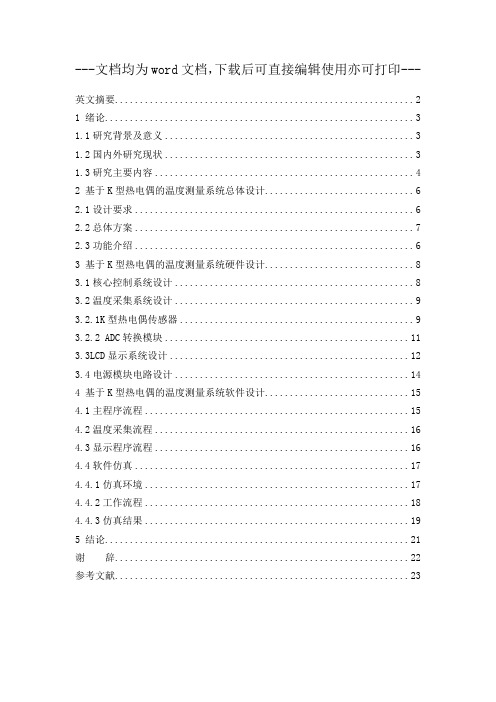
---文档均为word文档,下载后可直接编辑使用亦可打印---英文摘要 (2)1 绪论 (3)1.1研究背景及意义 (3)1.2国内外研究现状 (3)1.3研究主要内容 (4)2 基于K型热电偶的温度测量系统总体设计 (6)2.1设计要求 (6)2.2总体方案 (7)2.3功能介绍 (6)3 基于K型热电偶的温度测量系统硬件设计 (8)3.1核心控制系统设计 (8)3.2温度采集系统设计 (9)3.2.1K型热电偶传感器 (9)3.2.2 ADC转换模块 (11)3.3LCD显示系统设计 (12)3.4电源模块电路设计 (14)4 基于K型热电偶的温度测量系统软件设计 (15)4.1主程序流程 (15)4.2温度采集流程 (16)4.3显示程序流程 (16)4.4软件仿真 (17)4.4.1仿真环境 (17)4.4.2工作流程 (18)4.4.3仿真结果 (19)5 结论 (21)谢辞 (22)参考文献 (23)基于K型热电偶的温度测量系统设计摘要:K型热电偶不接触被测物中,目的是避免热平衡状态的变化,测量的敏感,响应速度快,良好的响应特性,常用于检测1000℃以上运动中的高温物体。
该测温系统结合单片机,设计以K型热电偶为温度传感器的温度测量系统。
其测量系统的测量温度可以分为三个档位,分别是高温档(500℃以上)中温档(100-500℃)低温档(100℃以下),使用前先预估待测物体温度选择合适的档位测量以提升测量精度。
通过温度传感器DS18B20在STM32L476芯片控制下进行实时温度检测并显示,能够实现快速测量环境温度。
关键词:单片机;热电偶;温度测量系统Design of temperature measurement system based on K-type thermocoupleAbstract:Non-contact temperature measurement will not be in contact with the measured object. It avoids changing the thermal equilibrium state of the object. It is sensitive when measuring. The response speed is fast and the response characteristics are good. It is usually used to detect high temperature objects in the movement of 1000°C and above. This text combines the advantage of the one-chip computer, design based on 51 one-chip computer non-contact temperature measurement system. Based on 51 single-chip non-contact temperature measurement system, the measurement temperature is divided into three gears, which are high temperature file (above 500°C), medium temperature file (100-500°C), low temperature file (below 100°C), and the object to be measured is estimated before use. Temperature Select the appropriate gear measurement to improve measurement accuracy. By using the STM32L476 chip to control the temperature sensor DS18B20 for real-time temperature detection and display, it is possible to quickly measure the ambient temperature.Keywords:single chip microcomputer; non-contact; temperature measurement; design基于K型热电偶的温度测量系统设计1 绪论1.1研究背景及意义当今社会,随着科学技术发展迅猛,社会生活水平也快速提高,企业对生产也有了更高的要求:信息化、科学化、自动化。
- 1、下载文档前请自行甄别文档内容的完整性,平台不提供额外的编辑、内容补充、找答案等附加服务。
- 2、"仅部分预览"的文档,不可在线预览部分如存在完整性等问题,可反馈申请退款(可完整预览的文档不适用该条件!)。
- 3、如文档侵犯您的权益,请联系客服反馈,我们会尽快为您处理(人工客服工作时间:9:00-18:30)。
ST STM32L476Gxx系列超低功耗MCU开发案
STM32L476Gxx器件是基于高性能ARM Cortex-M4 32位RISC核的超低功耗微控制器(MCU),工作频率高达80MHz。
Cortex-M4核具有单精度浮点单元(FPU),支持所有ARM单精度数据处理指令和数据类型。
它还实现了全套DSP指令和存储器保护单元(MPU),加强了应用安全。
STM32L476Gxx器件具有嵌入高速存储器(闪存高达1MB,SRAM高达128KB)、灵活的外接存储器控制器(FSMC)、Quad SPI闪存接口和各种增强的I/O和外设,连接2个APB总线、2个AHB总线和1个32位多AHB总线矩阵。
STM32L476Gxx器件为嵌入式闪存和SRAM嵌入了几种保护机制:读保护、写保护、专有代码读保护和防火墙。
这些器件还有三个快速12位ADC(5Msps)、两个比较器、两个运放、两个DAC通路、一个部基准电压缓冲器、一个低功耗RTC、两个通用32位计时器、两个马达控制专用16位PWM 计时器、七个通用16位计时器以及两个低功耗16位计时器。
这些器件支持外部sigma delta 调制器(DFSDM)的4个数字滤波器。
此外,还提供24条电容感应通路。
这些器件还嵌入了集成式LCD驱动器8×40或4×44,具有部设置转换器。
它们还具有标准和高级通信接口,包括:
3个I2C;
3个SPI;
3个USART、2个UART和1个低功耗UART;
2个SAI(串行音频接口);
1个SDMMC;
1个CAN;
1个USB OTG全速;
1个SWPMI(单线协议主接口);
STM32L476xx的工作温度围为-40℃~+85℃(结温+105℃)、-40℃~+105℃(结温+125℃)和-40℃~+125℃(结温+130℃),由1.71V~3.6V电源供电。
全面的节能模式实现了低功耗应用设计。
支持某些独立电源:ADC、DAC、OPAMP和比较器的模拟独立电源输入,USB的3.3V专用电源输入,14个I/O的独立供电电压低至1.08V。
V BAT输入支持RTC和备份寄存器。
STM32L476xx系列提供6种封装选项:64~144引脚封装。
STM32L476xx系列的主要特性
利用FlexPowerControl实现超低功耗
电源电压:1.71V~3.6V
温度围:-40℃~85℃/105℃/125℃
V BAT模式下的电流为300nA:为RTC和32位×32位备份寄存器供电
30nA关断模式(5个唤醒引脚)
120nA待机模式(5个唤醒引脚)
420nA待机模式+RTC
1.1μA Stop2模式,1.4μA Stop2 +RTC
100μA/MHz运行模式
批量采集模式(BAM)
4μs从停机模式唤醒
除关机以外的所有模式下的掉电复位(BOR)
互联矩阵
核:ARM 32位Cortex-M4 CPU,具有FPU、自适应实时加速器(ART Accelerator,能够从闪存实现零等待状态执行)和MPU,频率高达80MHz,性能高达
100DMIPS/1.25DMIPS/MHz(Dhrystone 2.1),采用DSP指令
时钟源
4MHz~48MHz晶体振荡器
RTC(LSE)的32kHz晶体振荡器
部16MHz工厂校准RC(±1%)
部低功耗32kHz RC(±5%)
部多速100kHz~48MHz振荡器,由LSE自动校准(精度优于±0.25%)
系统时钟的3个PLL、USB、音频ADC
RTC,具有HW日历、报警和校准功能
LCD 8×40或4×44,具有升压转换器
24条电容感应通路:支持触键、线性和旋转触摸传感器
16个计时器:2个16位高级马达控制、2个32位和5个16位通用、2个16位基础、2个低功耗16位计时器(停机模式)、2个看门狗、SysTick计时器
114个快速I/O,大多耐压5 V,14个I/O的独立电源电压低至1.08V;
存储器
1MB闪存,双库边写边读,专有代码写保护
128KB SRAM,具有32KB和硬件奇偶校验功能
静态存储器的外部存储器接口,支持SRAM、PSRAM、NOR和NAND存储器Quad SPI存储器接口
4个面向sigma delta调制器的数字滤波器
丰富的模拟外设(独立电源)
3个12位ADC,5Msps,高达16位,具有应用过采样功能,200μA/Msps 2个12位DAC,低功耗采样和保持
2个置有PGA的运放
2个超低功耗比较器
18个通信接口
USB OTG2.0全速、LPM和BCD
2个SAI(串行音频接口)
3个I2C FM+(1Mb/s)、SMBus/PMBus
6个USART(ISO 7816、LIN、IrDA、调制解调器)
3个SPI(4个SPI+Quad SPI)
CAN(2.0B Active)和SDMMC接口
SWPMI单线协议主I/F
14通路DMA控制器
真正的随机数发生器
CRC计算单元,96位唯一ID
开发支持:串行线调试(SWD)、JTAG、Embedded Trace Macrocell
图1 STM32L476xx系列框图
评估板STM32L476G-EVAL
STM32L476G-EVAL评估板设计用作意法半导体基于ARM Cortex-M4核的
STM32L476ZGT6微控制器的完整演示与开发平台,带有3个I²C总线、3个SPI和6个USART端口、CAN端口、SWPMI、2个SAI端口、12位ADC、12位DAC、LCD驱动器、部128KB SRAM和1MB闪存、Quad-SPI端口、触摸感应能力、USB OTG FS端口、LCD控制器、灵活的存储器控制器(FMC)、JTAG调试端口。
STM32L476G-EVAL可用
作用户应用开发的参考设计,虽然它并未视为最终应用。
评估板上的各种硬件特性有助于用户评估所有板载外设,例如USB、USART、数字麦克风、ADC和DAC、点矩阵TFT LCD、LCD玻璃模块、IrDA、LDR、SRAM、NOR闪存、Quad-SPI闪存、microSD卡、sigma-delta 调制器、采用SWP的智能卡、CAN收发器、EEPROM、RF-EEPROM。
扩展头让我们能够连接子板或者缠绕电路板。
主板上还整合了ST-LINK/V2-1在线调试器和闪烁装置。
图2 评估板STM32L476G-EVAL外形图
评估板STM32L476G-EVAL主要特性
STM32L476ZGT6微控制器,带有1MB闪存和128KB RAM
4种电源选项:电源插座、ST-LINK/V2-1 USB连接器、USB OTG FS连接器、子板
微控制器电源电压:3.3V或1.71V~3.6V
2个MEMS数字麦克风
2个具有独立音频容的立体声音频耳机插座输出
microSD卡槽,支持SD、SDHC、SDXC
附带4GB microSD卡
16Mb(1M×16位)SRAM器件
128Mb(8M×16位)NOR闪存
256M Quad-SPI闪存,具有双传输率(DTR)支持
RF-EEPROM,具有I²C总线
EEPROM,支持1MHz I²C总线通信速度
RS-232端口,可用于通信或MCU闪烁
IrDA收发器
USB OTG FS Micro-AB端口
CAN2.0A/B兼容端口
操纵杆,具有4路控制器和选择器
复位和唤醒/篡改按钮
触摸感应按钮
光敏电阻(LDR)
电位计
用于电源备份的纽扣电池
LCD玻璃模块子板(MB979),具有直接由STM32L476ZGT6驱动的40×8段LCD 2.8英寸320x240点矩阵彩色TFT LCD面板,具有电阻式触摸屏
智能卡连接器和SWP支持
NFC收发器连接器
用于ADC输入和DAC输出的连接器
利用双通路sigma-delta调制器实现电能计量演示
PT100热传感器,具有双通路sigma-delta调制器
MCU电流消耗测量电路
STM32L476ZGT6的比较器和运放
马达控制模块的扩展连接器
JTAG/SWD、ETM跟踪调试支持、带有USB虚拟COM端口的用户接口、嵌入式ST-LINK/V2-1调试与闪烁装置
子板的扩展连接器
图3 评估板STM32L476G-EVAL框图
图4 评估板STM32L476G-EVAL主要元件布局图。