富茁半导体MBR20150CT参数资料
MBR15XXCT中文资料
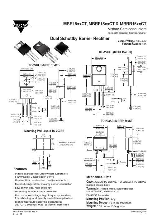
MBR15xxCT,MBRF15xxCT & MBRB15xxCTVishay Semiconductorsformerly General SemiconductorDocument Number Reverse Voltage 35 to 60VForward Current 15AMechanical DataCase:JEDEC TO-220AB, ITO-220AB & TO-263AB molded plastic bodyTerminals:Plated leads, solderable per MIL-STD-750, Method 2026Polarity:As marked Mounting Position:AnyMounting Torque:10 in-lbs maximum Weight:0.08 ounce, 2.24 gramsFeatures• Plastic package has Underwriters LaboratoryFlammability Classification 94V-0• Dual rectifier construction, positive center tap • Metal silicon junction, majority carrier conduction • Low power loss, high efficiency• Guardring for overvoltage protection• For use in low voltage, high frequency inverters,free wheeling, and polarity protection applications • High temperature soldering guaranteed:250°C/10 seconds, 0.25" (6.35mm) from caseMounting Pad Layout TO-263ABITO-220AB (MBRF15xxCT)TO-220AB (MBR15xxCT)TO-263AB (MBRB15xxCT)MBR15xxCT,MBRF15xxCT & MBRB15xxCTVishay Semiconductorsformerly General Semiconductor Document Number 88670Maximum Ratings(T C = 25°C unless otherwise noted)ParameterSymbol MBR1535CT MBR1545CT MBR1550CT MBR1560CT Unit Maximum repetitive peak reverse voltage V RRM 35455060V Working peak reverse voltage V RWM 35455060V Maximum DC blocking voltageV DC 35455060V Maximum average forward rectified current T otal device 15at TC = 105°C Per leg I F(AV)7.5A Peak repetitive forward current at T C = 105°C (rated V R , 20 KHz sq.wave)I FRM15APeak forward surge current8.3ms single half sine-wave superimposed I FSM 150A on rated load (JEDEC Method)Peak repetitive reverse surge current per leg at t p = 2.0µs, 1KH ZI RRM 1.00.5A Voltage rate of change (rated V R )dv/dt 10,000V/µs Operating junction temperature range T J –65 to +150°C Storage temperature rangeT STG –65 to +175°C RMS Isolation voltage (MBRF type only) from terminals to 4500 (NOTE 1)heatsink with t = 1.0 second, RH ≤30%V ISOL3500 (NOTE 2)V1500 (NOTE 3)Electrical Characteristics (T C = 25°C unless otherwise noted)ParameterSymbol MBR1535CT MBR1545CT MBR1550CT MBR1560CT UnitMaximum instantaneous forward voltage per leg (Note 4)at I F = 7.5A,T C = 25°C –0.75at I F = 7.5A,T C = 125°C V F 0.570.65Vat I F = 15A,T C = 25°C 0.84–at I F = 15A,T C =1 25°C 0.72–Maximum instantaneous reverse current T C = 25°C 0.1 1.0at rated DC blocking voltage per leg (Note 4)T C =125°CI R 1550mAThermal Characteristics (T C = 25°C unless otherwise noted)ParameterSymbol MBR MBRF MBRB Unit Maximum thermal resistance per legR ΘJA 60–60°C/WR ΘJC3.05.03.0Notes:(1) Clip mounting (on case), where lead does not overlap heatsink with 0.110”offset (2) Clip mounting (on case), where leads do overlap heatsink(3) Screw mounting with 4-40 screw, where washer diameter is ≤ 4.9 mm (0.19”)(4) Pulse test:300µs pulse width, 1% duty cycleOrdering InformationProductCase Package CodePackage OptionMBR1535CT - MBR1560CT TO-220AB 45Anti-Static tube, 50/tube, 2K/carton MBRF1535CT - MBRF1560CT ITO-220AB 45Anti-Static tube, 50/tube, 2K/carton 3113”reel, 800/reel, 4.8K/carton MBRB1535CT - MBRB1560CTTO-263AB45Anti-Static tube, 50/tube, 2K/carton 81Anti-Static 13”reel, 800/reel, 4.8K/cartonMBR15xxCT,MBRF15xxCT & MBRB15xxCTVishay Semiconductorsformerly General SemiconductorDocument Number Ratings andCharacteristic Curves (TA= 25°C unless otherwise noted)Case Temperature (°C)Fig. 1 – Forward CurrentDerating CurveA v e r a g e F o r w a r d C u r r e n t (A )Fig. 3 – Typical Instantaneous Forward Characteristics Per LegInstantaneous Forward Voltage (V)I n s t a n t a n e o u s F o r w a r d C u r r e n t (A )Percent of Rated Peak Reverse Voltage (%)I n s t a n t a n e o u s R e v e r s e C u r r e n t (m A )Fig. 4 – Typical Reverse Characteristics Per LegFig. 6 – Typical Transient ThermalImpedance Per Leg501001500510152025502575100125150175Number of Cycles at 60 H Zt, Pulse Duration (sec.)Fig. 2 – Maximum Non-Repetitive Peak Forward Surge Current Per LegP e a k F o r w a r d S u r g e C u r r e n t (A )0.010.1110500.0010.010.111050101001,0004,000Reverse Voltage (V)J u n c t i o n C a p a c i t a n c e (p F )T r a n s i e n t T h e r m a l I m p e d a n c e (°C W )Fig. 5 – Typical Junction Capacitance Per Leg0.010.11101000.1110100。
MBRS320;中文规格书,Datasheet资料
ACEx™ Bottomless™ CoolFET™ CROSSVOLT ™ DenseTrench™ DOME™ EcoSPARK™ E2CMOSTM EnSignaTM FACT™ FACT Quiet Series™
DISCLAIMER
FAST ® FASTr™ FRFET™ GlobalOptoisolator™ GTO™ HiSeC™ ISOPLANAR™ LittleFET™ MicroFET™ MicroPak™ MICROWIRE™
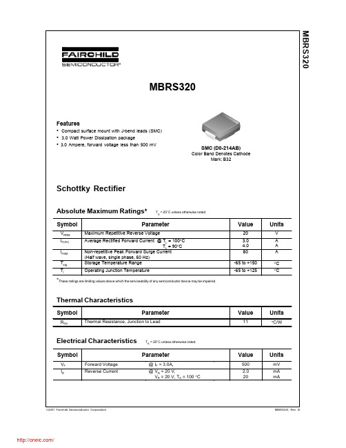
SMC (D0-214AB)
Color Band Denotes Cathode Mark: B32
Schottky Rectifier
Absolute Maximum Ratings*
Symbol
VRRM IF(AV) IFSM Tstg Tj
TA = 25°C unless otherwise noted
TA = 25°C unless otherwise noted
Parameter
@ IF = 3.0A, @ VR = 20 V, VR = 20 V, TA = 100 °C
Value
500 2.0 20
Units
mV mA mA
2001 child Semiconductor Corporation
Total Capacitance, CT [pF]
400 T A = +25 C 350 300 250 200 150 100 0 5 10 15 Reverse Voltage, VR [V] 20
Figure 3. Total Capacitance
2001 Fairchild Semiconductor Corporation
ASEMI肖特基二极管 MBR20200FCT图解 20A 200V

MBR20200FCT肖特基二极管,ASEMI品牌进口全新
型号:MBR20200FCT
品牌:ASEMI
封装:TO-220
特性:肖特基二极管
★电性参数:20A,200V
★芯片材质:SI
★正向电流(Io):20A
★芯片个数:2
★正向电压(VF):0.87V
★芯片尺寸:102MIL
★浪涌电流Ifsm:150A
★是否进口:是
★漏电流(Ir):10UA
★工作温度:-50~125
★恢复时间(Trr):<5nS
★引线数量:3
★编辑人:李绚
ASEMI品牌12年专业生产MBR20200FCT,拥有170人研发团队和8500㎡肖特基生产厂房,MBR20200FCT等肖特基均
采用俄罗斯Mikron芯片,28条台湾健鼎测试线,确保MBR20200FCT的高可靠性。
肖特基二极管MBR20200FCT参数规格:电流:20A ;电压:200V;管装:50/管;盒装:2000PCS/盒。
MBR20200FCT肖特基二极管广泛应用于开关电源、变频器、驱动器等电路,作高频、低压、大电流整流二极管、续流二极管、保护二极管使用,或在微波通信等电路中作整流二极管、小信号检波二极管使用。
欢迎咨询取样测试。
ASEMI整流小王子MBR10200FCT参数规格数据

编辑人:MM
摘要:肖特基二极管MBR10200FCT,选择ASEMI的理由不需要太多,一个就好!
肖特基二极管,市面上型号众多,品牌繁杂,我们选择时,考虑的因素也很多,MBR10200FCT是如何成为ASEMI品牌代表性的产品呢,本节就让我们来一探究竟:
MBR10200FCT其参数如下:
MBR10200FCT电压Vrrm:200V
MBR10200FCT电流If平均:10A
MBR10200FCT正向电压Vf最大:0.87V
MBR10200FCT电流,Ifs最大:150A
MBR10200FCT工作温度范围:-40°C to+150°C
MBR10200FCT封装形式:TO-220/TO-220F/ITO-220
MBR10200FCT反向恢复电流,Irrm:10UA
MBR10200FCT常用于开关电源的后端整流,ASEMI半导体拥台湾先进的健鼎一体化高速设备,同时检测产品12项参数,保障产品100%出厂合格,当然,ASEMI在封装工艺,原材料,
物流配送,等等方面均处于国际领先水平。
而这当中让ASEMI引以为豪的是米克朗芯片,这种芯片,无论是在稳定性还是在抗冲击能力上有着优于其它芯片的明显优势。
这也是国内外众多商家的所看重的。
ASEMI肖特基二极管型号大全,找找MBR4045PT属于哪一类

编辑:GGASEMI肖特基二极管的型号众多,接下来所列型号主要以电流电压大小,分为大类,再以封装区分作为辅助分类。
ASEMI肖特基二极管型号大全,找找MBR4045PT属于哪一类1A~5A 20V~150V 肖特基二极管两者型号都在用SS封装:SS110 、SS14 。
10A 45V~200V 肖特基二极管采用TO-220AC封装的有:MBR10200AC、MBR10150AC、MBR10100AC、MBR1060AC、MBR1045AC、MBR1040AC采用TO-220封装的有:MBR1040FCT、MBR10200FCT、MBR10100FCT、MBR10150FCT、 MBR1040CT、MBR10200CT、MBR1040FCT、MBT1045FCT、 MBR1045CT、MBR1040CT、 MBR1045CT、MBR1060CT、MBR1060FCT、MBR10100CT、MBT10100FCT、MBR10150CT该封装有FCT和CT结尾的型号命名,区别于前者是塑封封装、后者是铁头封装。
采用TO-251封装的有:BD1045CT、BD1060CT、BD10100CT、BD10150CT、BD10200CT、BD1040CT采用TO-252封装的有:BD1040CS、BD1045CS、BD1060CS、BD10100CS、BD10150CS、 BD10200CS 采用TO-263封装的有:MBR10200DC、MBR1040DC、MBR1045DC、MBR1060DC、MBR10100DC、MBR10150DC20A 45V~200V肖特基二极管采用TO-220AC封装的有:MBR20200AC、MBR20150AC、MBR20100AC、MBR2060AC、 MR2045AC采用TO-251封装的有:BD2060CT、BD2045CT、BD20100CT、BD20150CT、BD20200CT、采用TO-252封装的有:BD20100CS、BD20150CS、BD20200CS、BD2045CS、BD2060CS采用TO-263封装的有:MBR2045DC、MBR2060DC、MBR20100DC、MBR20150DC、MBR20200DC采用TO-220封装的有:MBR2045CT、MBR2045FCT、MBR20200FCT、MBR2060CT、 MBR20100FCT、MBR2060FCT、MBR20100CT、MBR20100FCT、 MBR20150CT、MBR20150FCT、MBR20200CT、MBR20200FCT采用TO-247/3封装的有:MBR20200PT30A 45V~200V 肖特基二极管采用TO-247/3P封装的有:MBR3045PT、MBR3060PT、MBR30100PT、MBR30150PT、MBR30200PT采用TO-263封装的有:MBR30200DC、MBR3060DC、MBR30100DC、MBR30150DC、MBR3045DC采用TO-220封装的有:MBR3045CT、MBR3045FCT、MBR3060CT、MBR3060FCT、MBR30100CT、MBT30100FCT、MBR30150CT、MBR30150FCT、 MBR30200CT、MBR30200FCT 40A 45V~200V 肖特基二极管采用TO-263封装的有:MBR4045DC、MBR40200DC、MBR4060DC、MBR40100DC、MBR40150DC采用TO-247/3P封装的有:MBR40200PT、MBR4045PT、MBR4060PT、MBR40100PT、 MBR40150PT、采用TO-220封装的有:MBR4045FCT、MBR4045CT、MBR4060FCT、MB40100FCT、 MBR4060CT、MBR40100CT60A 45V~220V 肖特基二极管采用TO-247/3P封装的有:MBR6045PT、MBR6060PT、MBR60100PT、MBR60150PT、 MBR60200PT 10A~60A 20V~100V 肖特基二极管采用ITO-220AB封装的有:SBT10150UCT、SBT10100UCT、SBT1060UCT、SBT1045UCT、SBT10150VCT、SBT10100VCT、SBT1060VCT、SBT1045VCT、SBT30150UCT、SBT2045VCT、SBT2060VCT、SBT20100VCT、SBT20150VCT、SBT2045UCT、 SBT2060UCT、SBT20100UCT、 SBT20150UCT、SBT3045VCT、SBT3060VCT、SBT30100VCT、 SBT30150VCT、SBT3045UCT、SBT3060UCT、SBT30100UCT、SBT1045UFCT、SBT30100UFCT、SBT1060UFCT、SBT10150VFCT、SBT10100VFCT、SBT1060VFCT、SBT1045VFCT、SBT10100UFCT、SBT2045VFCT、SBT10150UFCT、 SBT2060VFCT、SBT20100VFCT、SBT20150VFCT、SBT2045UFCT、SBT2060UFCT、SBT20100UFCT、SBT20150UFCT、SBT3045VFCT、SBT3060VFCT、SBT30100VFCT、 SBT30150VFCT、SBT3045UFCT、SBT3060UFCT、SBT30150UFCT、SBT1045UFCT、 SB10100LCT、SB10150LCT、SB1045LFCT、SB1045LFCT、SB30100LFCT、 SB1060LFCT、SB30150LFCT、SB10100LFCT、SB2045LFCT、SB10150LFCT、SB2060LFCT、SB20100LFCT、SB3060LCT采用TO-220AB封装的有:SB1060LCT、SB30150LCT、SB30150LCT、SB10100LCT、SB2060LCT、SB10150LCT、SB20150LCT、SB3060LCT、SB30100LCT、SB1045LCT采用TO-277封装的有:10V45这款肖特基二极管型号是超低压降、贴片小封装的。
MBR20100FCT ASEMI品牌肖特基二极管
MBR20100FCT ASEMI品牌肖特基二极管原装MBR20100FCT 型号:MBR20100FCT
品牌:ASEMI
封装:TO-220
特性:MBR20200FCT
电性参数:20A 100V
芯片材质:Mikron
正向电流(Io):20A
芯片个数:2
正向电压(VF):0.87V
芯片尺寸:102mil
浪涌电流Ifsm:150A
漏电流(Ir):150A
工作温度:-55~+150℃
恢复时间(Trr):>5nS
引线数量:3
ASEMI半导体厂家-强元芯电子专业经营分离式元器件,主要生产销售整流桥系列封装(DB、WOB、BR、KBPC、KBP、KBPM、GBU、GBL、KBL、KBJ、KBU);整流模块(MDS、MTC、MDQ、QLF、SQLF);汽车整流子(25A~50A STD&TVS Button、Cell、MUR);
肖特基二极管TO-220(MBR10100、10150、20100、20150、20200、30100、30200全塑封半塑封);肖特基TO-3P/247,整流二极管(STD、FR、HER、SF、SR、TVS、开关管、稳压管);玻璃钝化(GPP)六英寸晶圆等,各种封装参数在ASEMI都有详细介绍。
通富微电封装技术规格
通富微电是一家知名的半导体封装企业,其封装技术规格涵盖了多个方面。
以下是对其封装技术规格的简要介绍:1. 封装类型:通富微电具备多种封装类型的技术能力,包括但不限于DIP、SOP、SSOP、TSSOP、FLIPCHIP等。
这些类型分别对应不同的芯片尺寸和安装方式,能够满足不同应用场景的需求。
2. 尺寸精度:通富微电在封装过程中,对芯片和外壳的尺寸精度控制非常严格。
通过精密的定位和焊接技术,确保每个封装的芯片与外壳的尺寸和位置精度达到极高的标准,从而保证了产品的质量和性能。
3. 可靠性:通富微电在封装过程中,采用了一系列可靠性保障措施,如高温老化测试、长期可靠性测试等,以确保封装的芯片在长期使用中能够保持稳定和可靠的性能。
此外,公司还与合作伙伴共同开发了一系列耐高温、耐腐蚀、耐冲击的封装结构,提高了产品的可靠性和寿命。
4. 连接技术:通富微电在封装过程中,采用了一系列高性能的连接技术,如球栅列(BGA)、倒装芯片(FC)和电阻式键合(TAB)等。
这些连接技术能够实现芯片与外壳之间的电气和机械连接,确保了信号的传输质量和稳定性。
5. 环保材料:随着环保意识的提高,通富微电在封装过程中也注重环保材料的使用。
公司采用环保塑料外壳和无铅焊接材料,符合国家和国际环保标准,减少了产品对环境的影响。
6. 生产效率:通富微电通过自动化生产设备和生产流程的优化,提高了生产效率。
公司采用了先进的生产管理系统和生产设备,实现了高效的生产和质量控制,满足了客户对交货时间和产品质量的严格要求。
综上所述,通富微电的封装技术规格涵盖了多个方面,包括但不限于封装类型、尺寸精度、可靠性、连接技术、环保材料和生产效率等。
这些技术规格的保障,使得通富微电能够为客户提供高质量、可靠性和性能稳定的半导体产品。
士兰微 SBD20C150T F S 说明书
1. 原版
作 者: 殷资 作 者: 张科锋 作 者: 张科锋 作 者: 张科锋
杭州士兰微电子股份有限公司
http: //
版本号:2.0 共6页 第6页
额定值 2.0
包装 料管 料管 料管 料管 编带
单位 V A A C C
单位 C/W
杭州士兰微电子股份有限公司
http: //
版本号:2.1 共6页 第1页
电参数规格
参数名称 正向压降 反向漏电流
典型特性曲线
SBD20C150T/F/S 说明书
符号 VF IR
测试条件 IF=10A,TC=25C IF=10A,TC=125C VR=150V,TC =25C VR=150V,TC =125C
单位: mm
杭州士兰微电子股份有限公司
http: //
版本号:2.1 共6页 第4页
SBD20C150T/F/S 说明书
声明:
士兰保留说明书的更改权,恕不另行通知!客户在下单前应获取最新版本资料,并验证相关信息是否完整和最 新。
任何半导体产品特定条件下都有一定的失效或发生故障的可能,买方有责任在使用 Silan 产品进行系统设计和整 机制造时遵守安全标准并采取安全措施,以避免潜在失败风险可能造成人身伤害或财产损失情况的发生!
产品提升永无止境,我公司将竭诚为客户0T/F/S 版 权: 杭州士兰微电子股份有限公司
版 本: 2.1 修改记录:
1. 修改曲线 版 本: 2.0 修改记录:
1. 修改极限参数 版 本: 1.9 修改记录:
1. 修改典型特性曲线 2. 修改 TO-263-2L 封装外形图 版 本: 1.8 修改记录: 1. 修改 TO-220HW-3L 封装信息 2. 修改 TO-220-3L 封装信息 版 本: 1.7 修改记录: 1. 修改 TO-220F-3L 封装信息 2. 增加 TO-220HW-3L 封装 3. 增加 TO-263-2L 封装 版 本: 1.6 修改记录: 1. 修改产品规格分类 版 本: 1.5 修改记录: 1. 修改图 4 版 本: 1.4 修改记录: 1. 增加“正向平均整流电流”曲线 版 本: 1.3 修改记录: 1. 修改“封装外形图”
MBR20150
Summarize
Polarity
Symbol VRRM
VDC IFAV
MBR20150 150 150
20 10
Unit
A A ℃ ℃
Forward Peak Surge Current(Rated Load 8.3 Half Mssine Wave-According to JEDEC Method) Operating Junction Temperature Storage Temperature
公司地址:深圳市福田区华强北鼎城国际大厦1505室电话:86075566883108
Page 1
深圳市强元芯电子有限公司
Dual High-Voltage Schottky Rectifiers
The forward voltage and forward current curve
MBR20150
Absolute Maximum Ratings
Item Maximal Inverted Repetitive Peak Voltage
Maximal DC Interdiction Voltage Average Rectified Forward Current TC=150℃ Device unilateral Whole
Circuit and Protection Circuit.
■ MBR20150 Schottky diode,in the manufacture uses the main process technology includes: Silicon epitaxial substrate, P+ loop technology,The potential metal and the silicon alloy technology, the device uses the two chip, the common cathode, the plastic half package structure.
MBR20200CTP中文资料
MBR20200CTP SWITCHMODE™ PowerDual Schottky Rectifiering Schottky Barrier technology with a platinum barrier metal. This state–of–the–art device is designed for use in high frequency switching power supplies and converters with up to 48 volt outputs.They block up to 200 volts and offer improved Schottky performance at frequencies from 250 kHz to 5.0 MHz.•200 Volt Blocking Voltage•Low Forward V oltage Drop•Guardring for Stress Protection and High dv/dt Capability (10,000 V/µs)•Dual Diode Construction — Terminals 1 and 3 Must be Connected for Parallel Operation at Full RatingMechanical Characteristics•Case: Epoxy, Molded•Weight: 1.9 grams (approximately)•Finish: All External Surfaces Corrosion Resistant and Terminal Leads are Readily Solderable•Lead Temperature for Soldering Purposes:260°C Max. for 10 Seconds•Shipped 50 units per plastic tube•Marking: B20200PMAXIMUM RATINGS (Per Leg)Device Package Shipping ORDERING INFORMATIONMBR20200CTP TO–22050 Units/RailTHERMAL CHARACTERISTICS (Per Leg)ELECTRICAL CHARACTERISTICS (Per Leg)DYNAMIC CHARACTERISTICS (Per Leg)1001010.1i F , I N S T A N T A N E O U S F O R W A R D C U R R E N T (A )Figure 3. Typical Reverse Current V R , REVERSE VOLTAGE (VOLTS)Figure 4. Typical CapacitanceV R , REVERSE VOLTAGE (VOLTS)I R , R E V E R S E C U R R E N T (A )Figure 5. Current Derating, Case, Per Diode T C , CASE TEMPERATURE (°C)Figure 6. Forward Power Dissipation, Per DiodeI F(AV), AVERAGE FORWARD CURRENT (AMPS)I F (A V ), A V E R A G E F O R W A R D C U R R E N T (A )PACKAGE DIMENSIONSTO–220THREE–LEADTO–220ABCASE 221A–09ISSUE AASWITCHMODE is a trademark of Semiconductor Components Industries, LLC.ON Semiconductor and are trademarks of Semiconductor Components Industries, LLC (SCILLC). SCILLC reserves the right to make changes without further notice to any products herein. SCILLC makes no warranty, representation or guarantee regarding the suitability of its products for any particular purpose, nor does SCILLC assume any liability arising out of the application or use of any product or circuit, and specifically disclaims any and all liability, including without limitation special, consequential or incidental damages. “Typical” parameters which may be provided in SCILLC data sheets and/or specifications can and do vary in different applications and actual performance may vary over time. All operating parameters, including “Typicals” must be validated for each customer application by customer’s technical experts. SCILLC does not convey any license under its patent rights nor the rights of others.SCILLC products are not designed, intended, or authorized for use as components in systems intended for surgical implant into the body, or other applications intended to support or sustain life, or for any other application in which the failure of the SCILLC product could create a situation where personal injury or death may occur. Should Buyer purchase or use SCILLC products for any such unintended or unauthorized application, Buyer shall indemnify and hold SCILLC and its officers, employees, subsidiaries, affiliates, and distributors harmless against all claims, costs, damages, and expenses, and reasonable attorney fees arising out of, directly or indirectly, any claim of personal injury or death associated with such unintended or unauthorized use, even if such claim alleges that SCILLC was negligent regarding the design or manufacture of the part. SCILLC is an Equal Opportunity/Affirmative Action Employer. PUBLICATION ORDERING INFORMATIONCENTRAL/SOUTH AMERICA:Spanish Phone:303–308–7143 (Mon–Fri 8:00am to 5:00pm MST)Email:ONlit–spanish@Toll–Free from Mexico: Dial 01–800–288–2872 for Access –then Dial 866–297–9322ASIA/PACIFIC: LDC for ON Semiconductor – Asia SupportPhone:303–675–2121 (Tue–Fri 9:00am to 1:00pm, Hong Kong Time)Toll Free from Hong Kong & Singapore:001–800–4422–3781Email: ONlit–asia@JAPAN: ON Semiconductor, Japan Customer Focus Center4–32–1 Nishi–Gotanda, Shinagawa–ku, Tokyo, Japan 141–0031Phone: 81–3–5740–2700。
- 1、下载文档前请自行甄别文档内容的完整性,平台不提供额外的编辑、内容补充、找答案等附加服务。
- 2、"仅部分预览"的文档,不可在线预览部分如存在完整性等问题,可反馈申请退款(可完整预览的文档不适用该条件!)。
- 3、如文档侵犯您的权益,请联系客服反馈,我们会尽快为您处理(人工客服工作时间:9:00-18:30)。
100
50
FIG.5 - TYPICAL REVERSE
0 1 5 10 50 100
CHARACTERISTICS 100
NUMBER OF CYCLES AT 60Hz
FIG.4-TYPICAL JUNCTION CAPACITANCE
1400 1200 1000 800 600 400 200 0
REV 1.0 2015 JAN PAGE:2/2
FIG.3-MAXIMUM NON-REPETITIVE FORWARD SURGE CURRENT
250
0.1
PEAK FORWARD SURGE CURRENT,(A)
200
.01
.1
.3
.5
.7
.9
1.1
1.3
1.5
FORWARD VOLT AGE,(V)
150
Tj=25 C 8.3ms Single Half Sine Wave JEDEC method
.060 MAX. (1.5) .035 MAX. (0.9) .100 (2.54) PIN 1 PIN 3 Positive CT Suffix "C" + CASE PIN 2
.610 (15.5) MAX.
.550 (14.0) .158 (4.0) MIN. MAX. .114(2.9) .098(2.5) PIN 1 PIN 3 Negative CT Suffix "A" CASE PIN 2
Dimensions in inches and (millimeters)
MAXIMUM RATINGS AND ELECTRICAL CHARACTERISTICS
Rating 25 C ambient temperature uniess otherwies specified. Single phase half wave, 60Hz, resistive or inductive load. For capacitive load, derate current by 20%.
JUNCTION CAPACITANCE,(pF)
REVERSE LEAKAGE CURRENT, (mA)
10
1.0
Tj=75 C
.1
Tj=25 C
.01
.05
.1
.5
1
5
10
50
100
.01 0
20
40
60
80
100 120 140
REVERSE VOLTAGE,(V)
PERCENT OF RATED PEAK REVERSE VOLTAGE,(%)
20 AMP SCHOTTKY BARRIER RECTIFIERS
VOLTAGE RANGE
150 Volts
MBR20150CT
CURRENT FEATURES
* Low forward voltage drop * High current capability * High reliability * High surge current capability * Good for switching mode application
20.0 Amperes
ITO-220(FULLY INSULATED)
.412 (10.5) MAX. 3.4 f MAX. HOLE THRU .189 MAX. (4.8) .122 MAX. (3.1)
.108 (2.75)
.248 (6.3)
MECHANICAL DATA
* Case: Molded plastic * Epoxy: UL 94V-0 rate flame retardant * Lead: Lead solderable per MIL-STD-202, method 208 guranteed * Polarity: As Marked * Mounting position: Any * Weight: 2.05 grams
TYPE NUMBER
Maximum Recurrent Peak Reverse Voltage Maximum RMS Voltage Maximum DC Blocking Voltage Maximum Average Forward Rectified Current .375"(9.5mm) Lead Length at Tc=105 C Peak Forward Surge Current, 8.3 ms single half sine-wave superimposed on rated load (JEDEC method) Maximum Instantaneous Forward Voltage at 10A Maximum DC Reverse Current Ta=25 C at Rated DC Blocking Voltage Typical Junction Capacitance (Note1) Typical Thermal Resistance RqJA (Note 2) Operating Temperature Range TJ Storage Temperature Range TSTG
24 20
50
INSTANTANEOUS FORWARD CURRENT,(A)
16 12 8 4 0 0 20 40 60 80 100 120 140 160 180 200
10 5.0
1.0
Tj=25 C Pulse Width 300us 1% Duty Cycle
CASE TEMPERATURE,( C)
NOTES:
MBR20150CT 150 105 150 20 200 0.90 0.02 10 350 2.0 -55 +150 -55 +175
UNITS V V V A A V mA mA pF C/W C C
Ta=125 C
1. Measured at 1MHz and applied reverse voltage of 4.0V D.C. 2. Thermal Resistance Junction to Ambient Vertical PC Board Mounting 0.5"(12.7mm) Lead Length.
/2
RATING AND CHARACTERISTIC CURVES (MBR20150CT)
FIG.1-TYPICAL FORWARD CURRENT DERATING CURVE
AVERAGE FORWARD CURRENT,(A)
FIG.2-TYPICAL FORWARD CHARACTERISTICS