MTH01-SPI DATASHEET中英
STH10-SPI 温湿度传感器中英资料

- 完全可互换 - Small Size - 尺寸小 - Automatic Power Down - 自动断电
temperature compensation mechanism. Thus very high accurate reading of humidity in the full temperature range (0-50C) can be assured. 该STH10 是一款基于温度和相对湿度的传 感器模块,包括一个 SPI 接口(主模式)为 直接的温度和湿度读出。数字输出是预先计 算并无额外计算要求所必须的。改系统适用 于两个传感器要素:NTC 型高精度温度传 感器和电阻式相对湿度传感器来自日本。有 一个非常独特的专利和相对湿度的计算算 法,该系统通过良好的温度调节补偿机制可 以保证准确相对湿度输出。如此高精度读湿 度在整个温度范围( 0 - 50 C )都可以保 证。
2.2.3 SDAT SDAT is to transfer data to MCU. The SDAT line is valid after SCK goes high. Once data are all out, SDAT line will
Figure 2: Reduce IO Usage Application
mt8941中文资料_数据手册_IC数据表
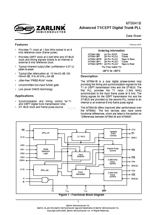
1Features•Provides T1 clock at 1.544 MHz locked to an 8 kHz reference clock (frame pulse)•Provides CEPT clock at 2.048 MHz and ST-BUS clock and timing signals locked to an internal or external 8 kHz reference clock•Typical inherent output jitter (unfiltered)= 0.07 UI peak-to-peak•Typical jitter attenuation at: 10 Hz=23 dB,100 Hz=43 dB, 5 to 40 kHz ≥ 64 dB •Jitter-free “FREE-RUN” mode •Uncommitted two-input NAND gate •Low power CMOS technologyApplications•Synchronization and timing control for T1 and CEPT digital trunk transmission links •ST- BUS clock and frame pulse sourceDescriptionThe MT8941B is a dual digital phase-locked loop providing the timing and synchronization signals for the T1 or CEPT transmission links and the ST-BUS. The first PLL provides the T1 clock (1.544 MHz)synchronized to the input frame pulse at 8 kHz. The timing signals for the CEPT transmission link and the ST-BUS are provided by the second PLL locked to an internal or an external 8 kHz frame pulse signal.The MT8941B offers improved jitter performance overthe MT8940. The two devices also have somefunctional differences, which are listed in the section on“Differences between MT8941B and MT8940”.February 2005Ordering InformationMT8941BE 24 Pin PDIP Tubes MT8941BP 28 Pin PLCC Tubes MT8941BPR 28 Pin PLCC Tape & Reel MT8941BP128 Pin PLCC*TubesMT8941BPR128 Pin PLCC*Tape & Reel*Pb Free Matte Tin-40°C to +85°CMT8941BAdvanced T1/CEPT Digital Trunk PLLData SheetFigure 1 - Functional Block DiagramF0iC12iMS0MS1MS2MS3C8KbC16iAi BiYoV DD V SSRSTCVb CV ENCVF0bC4b C4o ENC4o C2oC2o ENC2o2:1 MUXVariable Clock ControlMode Selection LogicDPLL #2Input SelectorClock GeneratorFrame Pulse Control4.096 MHz Clock Control2.048 MHz Clock ControlDPLL #1https://MT8941BData SheetFigure 2 - Pin ConnectionsPin DescriptionPin #Name DescriptionDIPPLCC11EN CV Variable clock enable (TTL compatible input) - This input directly controls the three statesof CV (pin 22) under all modes of operation. When HIGH, enables CV and when LOW, puts it in high impedance condition. It also controls the three states of CVb signal (pin 21) if MS1 is LOW. When ENCV is HIGH, the pin CVb is an output and when LOW, it is in high impedance state. However, if MS1 is HIGH, CVb is always an input.22MS0Mode select ‘0’ input (TTL compatible) - This input in conjunction with MS1 (pin 4) selects the major mode of operation for both DPLLs. (Refer to Tables 1 and 2.)33C12i 12.352 MHz Clock input (TTL compatible) - Master clock input for DPLL #1.46MS1Mode select-1 input (TTL compatible) - This input in conjunction with MS0 (pin 2) selects the major mode of operation for both DPLLs. (Refer to Tables 1 and 2.)57F0i Frame pulse input (TTL compatible) - This is the frame pulse input at 8 kHz. DPLL #1 locks to the falling edge of this input to generate T1 (1.544 MHz) clock.68F0bFrame pulse Bidirectional (TTL compatible input and Totem-pole output) - Depending on the minor mode selected for DPLL #2, it provides the 8 kHz frame pulse output or acts as an input to an external frame pulse.79MS2Mode select-2 input (TTL compatible) - This input in conjunction with MS3 (pin 17) selects the minor mode of operation for DPLL #2. (Refer to Table 3.)810C16i16.384 MHz Clock input (TTL compatible) - Master clock input for DPLL #2.911EN C4o Enable 4.096 MHz clock (TTL compatible input) - This active high input enables C4o (pin11) output. When LOW, the output C4o is in high impedance condition.1012C8Kb Clock 8 kHz Bidirectional (TTL compatible input and Totem-pole output) - This is the 8kHz input signal on the falling edge of which the DPLL #2 locks during its NORMAL mode. When DPLL #2 is in SINGLE CLOCK mode, this pin outputs an 8 kHz internal signal provided by DPLL #1 which is also connected internally to DPLL #2.28 PIN PLCC24 PIN PDIP123456789101112131415162423222120191817ENVC MS0C12i MS1F0i F0b MS2C16i ENC4o C8Kb C4o VSS VDD RST CV CVb Yo Bi Ai MS3ENC2o C2o C2o C4b456789101125242322212019•N C NC CVb Yo Bi Ai MS3ENC2oNC MS1F0i F0b MS2C16i ENC4o C 2o 32128272612131415161718C 12i M S 0E N C V VD D R S T C V C 8K b C 4o V S S C 4b C 2o N Chttps://MT8941B Data Sheet 1113C4o Clock 4.096 MHz (Three state output) - This is the inverse of the signal appearing on pin13 (C4b) at 4.096 MHz and has a rising edge in the frame pulse (F0b) window. The highimpedance state of this output is controlled by ENC4o (pin 9).1214V SS Ground (0 Volt)1315C4b Clock 4.096 MHz- Bidirectional (TTL compatible input and Totem-pole output) - When the mode select bit MS3 (pin 17) is HIGH, it provides the 4.096 MHz clock output with thefalling edge in the frame pulse (F0b) window. When pin 17 is LOW, C4b is an input to anexternal clock at 4.096 MHz.1416C2o Clock 2.048 MHz (Three state output) - This is the divide by two output of C4b (pin 13) and has a falling edge in the frame pulse (F0b) window. The high impedance state of this outputis controlled by EN C2o (pin 16).1517C2o Clock 2.048 MHz (Three state output) - This is the divide by two output of C4b (pin 13) and has a rising edge in the frame pulse (F0b) window. The high impedance state of this output iscontrolled by EN C2o (pin 16).1619EN C2o Enable 2.048 MHz clock (TTL compatible input) - This active high input enables both C2o and C2o outputs (pins 14 and 15). When LOW, these outputs are in high impedancecondition.1720MS3Mode select 3 input (TTL compatible) - This input in conjunction with MS2 (pin 7) selects the minor mode of operation for DPLL #2. (Refer to Table 3.)18, 1921,22Ai, Bi Inputs A and B (TTL compatible) -These are the two inputs of the uncommitted NAND gate.2023Y o Output Y (Totem pole output) - Output of the uncommitted NAND gate.2124CVb Variable clock Bidirectional (TTL compatible input and Totem-pole output) - When acting as an output (MS1-LOW) during the NORMAL mode of DPLL #1, this pin provides the1.544 MHz clock locked to the input frame pulse F0i (pin 5). When MS1 is HIGH, it is aninput to an external clock at 1.544 MHz or 2.048 MHz to provide the internal signal at 8 kHzto DPLL #2.2226CV Variable clock (Three state output) - This is the inverse output of the signal appearing on pin 21, the high impedance state of which is controlled by EN CV (pin 1).2327RST Reset (Schmitt trigger input) - This input (active LOW) puts the MT8941B in its reset state.To guarantee proper operation, the device must be reset after power-up. The time constantfor a power-up reset circuit (see Figures 9-13) must be a minimum of five times the rise timeof the power supply. In normal operation, the RST pin must be held low for a minimum of60nsec to reset the device.2428V DD V DD (+5 V) Power supply.4, 5, 18, 25NC No Connection.Pin Description (continued)Pin #Name DescriptionDIP PLCChttps://MT8941BData SheetFunctional DescriptionThe MT8941B is a dual digital phase-locked loop providing the timing and synchronization signals to the interface circuits for T1 and CEPT (30+2) Primary Multiplex Digital Transmission links. As shown in the functional block diagram (see Figure 1), the MT8941B has two digital phase-locked loops (DPLLs), associated output controls and the mode selection logic circuits. The two DPLLs, although similar in principle, operate independently to provide T1(1.544 MHz) and CEPT (2.048 MHz) transmission clocks and ST-BUS timing signals.The principle of operation behind the two DPLLs is shown in Figure 3. A master clock is divided down to 8 kHz where it is compared with the 8 kHz input, and depending on the output of the phase comparison, the master clock frequency is corrected.Figure 3 - DPLL PrincipleThe MT8941B achieves the frequency correction in both directions by using three methods; speed-up, slow-down and no-correction.As shown in Figure 4, the falling edge of the 8 kHz input signal (C8Kb for DPLL #2 or F0i for DPLL # 1) is used to sample the internally generated 8 kHz clock and the correction signal (CS) once in every frame (125 µs). If the sampled CS is “1”, then the DPLL makes a speed-up or slow-down correction depending upon the sampled value of the internal 8 kHz signal. A sampled ”0” or “1” causes the frequency correction circuit to respectively stretch or shrink the master clock by half a period at one instant in the frame. If the sampled CS is “0”, then the DPLL makes no correction on the master clock input. Note that since the internal 8 kHz signal and the CS signal are derived from the master clock, a correction will cause both clocks to stretch or shrink simultaneously by an amount equal to half the period of the master clock.Once in synchronization, the falling edge of the reference signal (C8Kb or F0i) will be aligned with either the falling or the rising edge of CS. It is aligned with the rising edge of CS when the reference signal is slower than the internal 8 kHz signal. On the other hand, the falling edge of the reference signal will be aligned with the falling edge of CS if the reference signal is faster than the internal 8 kHz signal.Figure 4 - Phase ComparisonMaster clock(12.352 MHz / 16.384 MHz)Frequency Correction÷ 8Output(1.544 MHz / 2.048 MHz)Input (8 kHz)Phase Comparison ÷ 193 /÷ 256C8Kb (DPLL #2)or F0i (DPLL #1)sampling edgeInterna l 8 kHzcorrectioncorrectionCS speed-up regionslow-down regiont CSt CSFno-correctionF0b(DPLL #2)DPLL #1: DPLL #2:t CSF = 766 × T P16where, T P12 is the 12.352 MHz master clock oscillator period for DPLL #1 and T P16 is the 16.384 MHz master clock period for DPLL #2.t CS = 4 × T P12 ± 0.5 × T P12t CS = 512 × T P16 ± 0.5 × T P16https://MT8941B Data SheetInput-to-Output Phase RelationshipThe no-correction window size is 324 ns for DPLL #1 and 32 µs for DPLL #2. It is possible for the relative phase of the reference signal to swing inside the no-correction window depending on its jitter and the relative drift of the master clock. As a result, the phase relationship between the input signal and the output clocks (and frame pulse in case of DPLL #2) may vary up to a maximum of window size. This situation is illustrated in Figure 4. The maximum phase variation for DPLL #1 is 324 ns and for DPLL #2 it is 32 µs. However, this phase difference can be absorbed by the input jitter buffer of Zarlink’s T1/CEPT devices.The no-correction window acts as a filter for low frequency jitter and wander since the DPLL does not track the reference signal inside it. The size of the no-correction window is less than or equal to the size of the input jitter buffer on the T1 and CEPT devices to guarantee that no slip will occur in the received T1/CEPT frame.The circuit will remain in synchronization as long as the input frequency is within the lock-in range of the DPLLs (refer to the section on “Jitter Performance and Lock-in Range” for further details). The lock-in range is wide enough to meet the CCITT line rate specification (1.544 MHz ±32 ppm and 2.048 MHz ±50 ppm) for the High Capacity Terrestrial Digital Service.The phase sampling is done once in a frame (8 kHz) for each DPLL. The divisions are set at 8 and 193 for DPLL #1, which locks to the falling edge of the input at 8 kHz to generate T1 (1.544 MHz) clock. For DPLL #2, the divisions are set at 8 and 256 to provide the CEPT/ST-BUS clock at 2.048 MHz synchronized to the falling edge of the input signal (8 kHz). The master clock source is specified to be 12.352 MHz for DPLL #1 and 16.384 MHz for DPLL #2 over the entire temperature range of operation.The inputs MS0 to MS3 are used to select the operating mode of the MT8941B, see Tables 1 to 4. All the outputs are controlled to the high impedance condition by their respective enable controls. The uncommitted NAND gate is available for use in applications involving Zarlink’s MT8976/ MH89760 (T1 Interfaces) and MT8979/MH89790 https://(CEPT Interfaces).Modes of OperationThe operation of the MT8941B is categorized into major modes and minor modes. The major modes are defined for both DPLLs by the mode select pins MS0 and MS1. The minor modes are selected by pins MS2 and MS3 and are applicable only to DPLL #2. There are no minor modes for DPLL #1.Major modes of DPLL #1DPLL #1 can be operated in three major modes as selected by MS0 and MS1 (Table 1). When MS1 is LOW, it is in NORMAL mode, which provides a T1 (1.544 MHz) clock signal locked to the falling edge of the input frame pulse F0i (8 kHz). DPLL #1 requires a master clock input of 12.352 MHz (C12i). In the second and third major modes (MS1 is HIGH), DPLL #1 is set to DIVIDE an external 1.544 MHz or 2.048 MHz signal applied at CVb (pin 21). The division can be set by MS0 to be either 193 (LOW) or 256 (HIGH). In these modes, the 8 kHz output at C8Kb is connected internally to DPLL #2, which operates in SINGLE CLOCK mode.Major modes of DPLL #2There are four major modes for DPLL #2 selectable by MS0 and MS1, as shown in Table 2. In all these modes DPLL #2 provides the CEPT PCM30 timing, and the ST-BUS clock and framing signals.In NORMAL mode, DPLL #2 provides the CEPT/ST-BUS compatible timing signals locked to the falling edge of the 8 kHz input signal (C8Kb). These signals are 4.096 MHz (C4o and C4b) and 2.048 MHz (C2o and C2o) clocks, and the 8 kHz frame pulse (F0b) derived from the 16.384 MHz master clock. This mode can be the same as the FREE-RUN mode if the C8Kb pin is tied to V DD or V SS.MT8941BData SheetTable 1 - Major Modes of DPLL #1Table 2 - Major Modes of DPLL #2M S 0M S 1Mode of Operation FunctionX 0NORMAL Provides the T1 (1.544 MHz) clock synchronized to the falling edge of the input frame pulse (F0i).01DIVIDE-1DPLL #1 divides the CVb input by 193. The divided output is connected to DPLL #2.11DIVIDE-2DPLL #1 divides the CVb input by 256. The divided output is connected to DPLL #2.Note:X: indicates don’t careM S 0M S 1Mode of Operation FunctionNORMALProvides CEPT/ST-BUS timing signals locked to the falling edge of the 8 kHz input signal at C8Kb.10FREE-RUN Provides CEPT/ST-BUS timing and framing signals with no external inputs, except themaster clock.1SINGLECLOCK-1Provides CEPT/ST-BUS timing signals locked to the falling edge of the 8 kHz internal signal provided by DPLL #1.11SINGLE CLOCK-2Provides CEPT/ST-BUS timing signals locked to the falling edge of the 8 kHz internal signal provided by DPLL #1.https://MT8941BData SheetTable 3 - Minor Modes of DPLL #2In FREE-RUN mode, DPLL #2 generates the stand-alone CEPT and ST-BUS timing and framing signals with no external inputs except the master clock set at 16.384 MHz. The DPLL makes no correction in this configuration and provides the timing signals without any jitter.The operation of DPLL #2 in SINGLE CLOCK-1 mode is identical to SINGLE CLOCK-2 mode, providing the CEPT and ST-BUS compatible timing signals synchronized to the internal 8 kHz signal obtained from DPLL#1 in DIVIDE mode. When SINGLE CLOCK-1 mode is selected for DPLL #2, it automatically selects the DIVIDE-1 mode for DPLL #1, and thus, an external 1.544 MHz clock signal applied at CVb (pin 21) is divided by DPLL #1 to generate the internal signal at 8 kHz on to which DPLL #2 locks. Similarly when SINGLE CLOCK-2 mode is selected, DPLL #1 is in DIVIDE-2 mode, with an external signal of 2.048 MHz providing the internal 8 kHz signal to DPLL #2. In both these modes, this internal signal is available on C8Kb (pin 10) and DPLL #2 locks to the falling edge to provide the CEPT and ST-BUS compatible timing signals. This is in contrast to the Normal mode where these timing signals are synchronized with the falling edge of the 8 kHz signal on C8Kb. Minor modes of DPLL #2The minor modes for DPLL #2 depends upon the status of the mode select bits MS2 and MS3 (pins 7 and 17).M S 2M S 3Functional Description11Provides CEPT/ST-BUS 4.096 MHz and 2.048 MHz clocks and 8kHz frame pulse depending on the major mode selected.01Provides CEPT/ST-BUS 4.096 MHz & 2.048 MHz clocksdepending on the major mode selected while F0b acts as an input. However, the input on F0b has no effect on the operation of DPLL #2 unless it is in FREE-RUN mode.00Overrides the major mode selected and accepts properly phase related external 4.096 MHz clock and 8 kHz frame pulse to provide the ST-BUS compatible clock at 2.048 MHz.10Overrides the major mode selected and accepts a 4.096 MHz external clock to provide the ST-BUS clock and frame pulse at 2.048 MHz and 8 kHz, respectively.https://MT8941BData SheetTable 4 - Summary of Modes of Operation - DPLL #1 and #2When MS3 is HIGH, DPLL #2 operates in any of the major modes selected by MS0 and MS1. When MS3 is LOW,it overrides the major mode selected and DPLL#2 accepts an external clock of 4.096 MHz on C4b (pin 13) to provide the 2.048 MHz clocks (C2o and C2o) and the 8 kHz frame pulse (F0b) compatible with the ST-BUS format.The mode select bit MS2 controls the direction of the signal on F0b (pin 6).When MS2 is LOW, the F0b pin is an 8 kHz frame pulse input. This input is effective only when MS3 is also LOW and pin C4b is fed by a 4.096 MHz clock, which has a proper phase relationship with the signal on F0b (refer Figure 18). Otherwise, the input on pin F0b will have no bearing on the operation of DPLL #2, unless it is in FREE-RUN mode as selected by MS0 and MS1. In FREE-RUN mode, the input on F0b is treated the same way as the C8Kb input is in NORMAL mode. The frequency of the signal on F0b should be 16 kHz for DPLL #2 to lock and generate the ST-BUS compatible clocks at 4.096 MHz and 2.048 MHz.Mode #M S 0M S 1M S 2M S 3Operating ModesDPLL #1DPLL #200000NORMAL MODE:Provides the T1 (1.544 MHz) clocksynchronized to the falling edge of the input frame pulse (F0i).Properly phase related External 4.096 MHzclock and 8 kHz frame pulse provide the ST-BUS clock at 2.048 MHz.10001NORMAL MODE NORMAL MODE:F0b is an input but has no function in this mode.21NORMAL MODE External 4.096 MHz provides the ST-BUS clock and Frame Pulse at 2.048 MHz and 8 kHz, respectively.30011NORMAL MODENORMAL MODE:Provides the CEPT/ST-BUS compatible timing signals locked to the 8 kHz input signal (C8Kb).40100DIVIDE-1 MODE Same as mode ‘0’.50101DIVIDE-1 MODE SINGLE CLOCK-1 MODEF0b is an input but has no function in this mode.611DIVIDE-1 MODESame as mode 2.70111DIVIDE-1 MODE:Divides the CVb input by 193. The divided output is connected to DPLL #2.SINGLE CLOCK-1 MODE:Provides the CEPT/ST-BUS compatible timing signals locked to the 8 kHz internal signal provided by DPLL #1.81000NORMAL MODESame as mode ‘0’.91001NORMAL MODEF0b is an input and DPLL #2 locks on toit only if it is at 16 kHz to provide the ST-BUS control signals.1011NORMAL MODE Same as mode 2.111011NORMAL MODEFREE-RUN MODE:Provides the ST-BUS timing signals with no external inputs except the master clock.121100DIVIDE-2 MODE Same as mode ‘0’.131101DIVIDE-2 MODE SINGLE CLOCK-2 MODE:F0b is an input but has no function in this mode.14111DIVIDE-2 MODESame as mode 2.151111DIVIDE-2 MODE:Divides the CVb input by 256. The divided output is connected to DPLL#2.SINGLE CLOCK-2 MODE:Provides the CEPT/ST-BUS compatible timing signals locked to the 8 kHz internal signal provided by DPLL #1.https://MT8941BData SheetWhen MS2 is HIGH, the F0b pin provides the frame pulse output compatible with the ST-BUS format and locked to the internal or external input signal as determined by the other mode select pins.Table 4 summarizes the modes of the two DPLL. It should be noted that each of the major modes selected for DPLL #2 can have any of the minor modes, although some of the combinations are functionally similar. The required operation of both DPLL #1 and DPLL #2 must be considered when determining MS0-MS3.Table 5 - Functions of the Bidirectional Signals in Each ModeThe direction and frequency of each of the bidirectional signals are listed in Table 5 for each of the given modes in Table 4.Jitter Performance and Lock-in RangeThe output jitter of a DPLL is composed of the intrinsic jitter, measured when no jitter is present at the input, and the output jitter resulting from jitter on the input signal. The spectrum of the intrinsic jitter for both DPLLs of the MT8941B is shown in Figure 5. The typical peak-to-peak value for this jitter is 0.07UI. The transfer function, which is the ratio of the output jitter to the input jitter (both measured at a particular frequency), is shown in Figure 6 for DPLL #1 and Figure 7 for DPLL #2. The transfer function is measured when the peak-to-peak amplitude of the sinusoidal input jitter conforms to the following:10 Hz - 100 Hz : 13.6 µs100 Hz - 10 kHz : 20 dB/decade roll-off > 10 kHz : 97.2 nsThe ability of a DPLL to phase-lock the input signal to the reference signal and to remain locked depends upon its lock-in range. The lock-in range of the DPLL is specified in terms of the maximum frequency variation in the 8 kHz reference signal. It is also directly affected by the oscillator frequency tolerance. Table 6 lists different values for the lock-in range and the corresponding oscillator frequency tolerance for DPLL #1 and DPLL #2. The smaller the tolerance value, the larger the lock-in range.Mode #F0b (kHz)C4b (MHz)C8Kb (kHz)CVb (MHz)0i:8i:4.096i:X o:1.5441i:X o:4.096i:8o:1.5442o:8i:4.096i:X o:1.5443o:8o:4.096i:8o:1.5444i:8i:4.096i:X i:1.5445i:X o:4.096o:8i:1.5446o:8i:4.096i:X i:1.5447o:8o:4.096o:8i:1.5448i:8i:4.096i:X o:1.5449i:16o:4.096i:X o:1.54410o:8i:4.096i:X o:1.54411o:8o:4.096i:X o:1.54412i:8i:4.096i:X i:2.40813i:X o:4.096o:8i:2.40814o:8i:4.096i:X i:2.40815o:8o:4.096o:8i:2.408Note:i: Inputo: OutputX: “don’t care” input. Connect to V DD or V SS.https://MT8941BData SheetThe T1 and CEPT standards specify that, for free running equipment, the output clock tolerance must be less than or equal to ±32ppm and ±50ppm respectively. This requirement restricts the oscillators of DPLL #1 and DPLL #2to have maximum tolerances of ±32ppm and ±50ppm respectively.Table 6 - Lock-in Range vs. Oscillator Frequency ToleranceFigure 5 - The Spectrum of the Inherent Jitter for either PLLOscillator Clock* Tolerance (±ppm)Lock-in Range (±Hz)DPLL #1DPLL #25 2.55 1.9110 2.51 1.8720 2.43 1.7932 2.33 1.6950 2.19 1.55100 1.79 1.15150 1.39.751751.19.55Note:* Please refer to the section on “Jitter Performance and Lock-inRange” for recommended oscillator tolerances for DPLL #1 & #2.https://MT8941B Data SheetFigure 6 - The Jitter Transfer Function for PLL1https://Figure 7 - The Jitter Transfer Function for PLL2However, if DPLL #1 and DPLL #2 are daisy-chained as shown in Figures 9 and 10, the output clock tolerance of DPLL #1 will be equal to that of the DPLL #2 oscillator when DPLL #2 is free-running. In this case, the oscillator tolerance of DPLL #1 has no impact on its output clock tolerance. For this reason, it is recommended to use a ±32ppm oscillator for DPLL #2 and a ±100 ppm oscillator for DPLL #1.MT8941BData SheetDifferences between MT8941B and MT8940The MT8941B and MT8940 are pin and mode compatible for most applications. However, the user should take note of the following differences between the two parts.Figure 8 - Application Differences between the MT8940 and MT8941Ba) Distributed TimingM U XMT8940MT89408 kHz Reference Signal8 kHz Reference SignalLine Card 1ClocksLine Card nClocksData BusLine Card 1Line Card nMT8941BM U X8 kHz Reference Signal8 kHz Reference SignalClocksb) Centralized TimingData Bushttps://MT8941B Data Sheet Besides the improved jitter performance, the MT8941B differs from the MT8940 in five other areas:1.Input pins on the MT8941B do not incorporate internal pull-up or pull-down resistors. In addition, the output con-figuration of the bidirectional C8Kb pin has been converted from an open drain output to a Totem-pole output.2.The MT8941B includes a no-correction window to filter out low frequency jitter and wander as illustrated in Fig-ure 4. Consequently, there is no constant phase relationship between reference signal F0i of DPLL # 1 or C8Kb of DPLL #2 and the output clocks of DPLL #1 or DPLL #2. Figure 4 shows the new phase relationship between C8Kb and the DPLL #2 output clocks. Figure 8 illustrates an application where the MT8941B cannot replace the MT8940 and suggests an alternative solution.3.The MT8941B must be reset after power-up in order to guarantee proper operation, which is not the case for theMT8940.4.For the MT8941B, DPLL #2 locks to the falling edge of the C8Kb reference signal. DPLL#2 of the MT8940locks on to the rising edge of C8Kb.5.While the MT8940 is available only in a 24 pin plastic DIP, the MT8941B has an additional 28 pin PLCC packageoption.ApplicationsThe following figures illustrate how the MT8941B can be used in a minimum component count approach in providing the timing and synchronization signals for the Zarlink T1 or CEPT interfaces, and the ST-BUS. The hardware selectable modes and the independent control over each PLL adds flexibility to the interface circuits. It can be easily reconfigured to provide the timing and control signals for both the master and slave ends of the link.https://Synchronization and Timing Signals for the T1 Transmission LinkFigures 9 and 10 show examples of how to generate the timing signals for the master and slave ends of a T1 link. At the master end of the link (Figure 9), DPLL #2 is the source of the ST-BUS signals derived from the crystal clock. The frame pulse output is looped back to DPLL #1 (in NORMAL mode), which locks to it to generate the T1 line clock. The timing relationship between the 1.544 MHz T1 clock and the 2.048 MHz ST-BUS clock meets the requirements of the MH89760/760B. The crystal clock at 12.352 MHz is used by DPLL #1 to generate the 1.544 MHz clock, while DPLL #2 (in FREE-RUN mode) uses the 16.384 MHz crystal oscillator to generate the ST-BUS clocks for system timing. The generated ST-BUS signals can be used to synchronize the system and the switching equipment at the master end.MT8941BData SheetFigure 9 - Synchronization at the Master End of the T1 Transmission LinkFigure 10 - Synchronization at the Slave End of the T1 Transmission LinkCrystal Clock(16.384 MHz)Crystal Clock(12.352 MHz)MT8941B MS0MS1MS2MS3F0i C12i EN CV C8Kb C16i EN C4o EN C2oV SSV DDCVbC4b C2oF0b RSTMH89760BC1.5i C2iF0iDSTi DSTo CSTi CSTo TxT TxR RxT RxRMT8980/81ST-BUS SWITCHT1LINK(1.544 Mbps)TRANSMITRECEIVE Mode of Operation for the MT8941BDPLL #1 - NORMAL (MS0 = X; MS1 = 0)DPLL #2 - FREE-RUN (MS0=1; MS2=1; MS3=1)V DDRCCrystal Clock(16.384 MHz)Crystal Clock(12.352 MHz)MT8941B MS0MS1MS2MS3F0i C12i EN CV C8Kb C16i EN C4o EN C2oV SSV DDCVbC4b C2o F0bRSTMH89760B C1.5i C2iF0i DSTi DSTo CSTi CSTo TxT TxR RxT RxRMT8980/81ST-BUS SWITCHT1LINK (1.544 Mbps)TRANSMITRECEIVEMode of Operation for the MT8941BDPLL #1 - NORMAL (MS1=0)DPLL #2 - NORMAL (MS0=0; MS1=0; MS2=1; MS3=1)V DDRCE8Kohttps://。
ICS557-01 Datasheet说明书

PCI-EXPRESS CLOCK SOURCEDescriptionThe ICS557-01 is a clock chip designed for use inPCI-Express Cards as a clock source. It provides a pair of differential outputs at 100 MHz in a small 8-pin SOIC package.Using IDT’s patented Phase-Locked Loop (PLL) techniques, the device takes a 25 MHz crystal input and produces HCSL (Host Clock Signal Level) differential outputs at 100 MHz clock frequency. LVDS signal levels can also be supported via an alternative termination scheme.Features•Supports PCI-Express TM HCSL Outputs0.7 V current mode differential pair •Supports LVDS Output Levels•Packaged in 8-pin SOIC•RoHS 5 (green ) or RoHS 6 (green and lead free) compliant packaging•Operating voltage of 3.3 V•Low power consumption•Input frequency of 25 MHz•Short term jitter 100 ps (peak-to-peak)•Output Enable via pin selection•Industrial temperature range availableBlock DiagramPin Assignment Pin DescriptionsPin NumberPinNamePinTypePin Description1OE Input Output Enable signal(H = outputs are enabled, L = outputs are disabled/tristated).Internal pull-up resistor.2X1Input Crystal or clock input. Connect to a 25 MHz crystal or single ended clock. 3X2XO Crystal Connection. Connect to a parallel mode crystal.Leave floating if clock input.4GND Power Connect to ground.5IREF Output A 475Ω precision resistor connected between this pin and groundestablishes the external reference current.6CLK Output HCSL differential complementary clock output.7CLK Output HCSL differential clock output.8VDD Power Connect to +3.3 V.Applications Information External ComponentsA minimum number of external components are required for proper operation.Decoupling CapacitorsDecoupling capacitors of 0.01 μF should be connected between VDD and the ground plane (pin 4) as close to the VDD pin as possible. Do not share ground vias between components. Route power from power source through the capacitor pad and then into IDT pin.CrystalA 25 MHz fundamental mode parallel resonant crystal with C L = 16 pF should be used. This crystal must have less than 300 ppm of error across temperature in order for theICS557-01 to meet PCI Express specifications.Crystal CapacitorsCrystal capacitors are connected from pins X1 to ground and X2 to ground to optimize the accuracy of the output frequency.C L= Crystal’s load capacitance in pFCrystal Capacitors (pF) = (C L- 8) * 2For example, for a crystal with a 16 pF load cap, each external crystal cap would be 16 pF. (16-8)*2=16.Current Source (Iref) Reference Resistor - R RIf board target trace impedance (Z) is 50Ω, then R R = 475Ω(1%), providing IREF of 2.32 mA. The output current (I OH) is equal to 6*IREF.Output TerminationThe PCI-Express differential clock outputs of the ICS557-01 are open source drivers and require an external series resistor and a resistor to ground. These resistor values and their allowable locations are shown in detail in thePCI-Express Layout Guidelines section.The ICS557-01can also be configured for LVDS compatible voltage levels. See the LVDS Compatible Layout Guidelines sectionGeneral PCB Layout RecommendationsFor optimum device performance and lowest output phase noise, the following guidelines should be observed.1. Each 0.01µF decoupling capacitor should be mounted on the component side of the board as close to the VDD pin as possible.2. No vias should be used between decoupling capacitor and VDD pin.3. The PCB trace to VDD pin should be kept as short as possible, as should the PCB trace to the ground via. Distance of the ferrite bead and bulk decoupling from the device is less critical.4. An optimum layout is one with all components on the same side of the board, minimizing vias through other signal layers (any ferrite beads and bulk decoupling capacitors can be mounted on the back). Other signal traces should be routed away from the ICS557-01.This includes signal traces just underneath the device, or on layers adjacent to the ground plane layer used by the device.PCI-Express Layout GuidelinesFigure 1: PCI-Express Device RoutingTypical PCI-Express (HCSL) WaveformLVDS Compatible Layout GuidelinesFigure: LVDS Device RoutingTypical LVDS WaveformAbsolute Maximum RatingsStresses above the ratings listed below can cause permanent damage to the ICS557-01. These ratings are stress ratings only. Functional operation of the device at these or any other conditions above those indicated in the operational sections of the specifications is not implied. Exposure to absolute maximum rating conditions for extended periods can affect product reliability. Electrical parameters are guaranteed only over the recommended operating temperature range.DC Electrical CharacteristicsUnless stated otherwise, VDD = 3.3 V ±5%, Ambient Temperature -40 to +85°C1 Single edge is monotonic when transitioning through region.2 Inputs with pull-ups/-downs are not included.ItemRatingSupply Voltage, VDD, VDDA 5.5 VAll Inputs and Outputs-0.5 V to VDD+0.5 V Ambient Operating Temperature (commercial)0 to +70°C Ambient Operating Temperature (industrial)-40 to +85°C Storage Temperature -65 to +150°C Junction Temperature 125°C Soldering Temperature 260°CESD Protection (Input)2000 V min. (HBM)ParameterSymbolConditions Min.Typ.Max.UnitsSupply Voltage V 3.135 3.465Input High Voltage 1V IH 2.0VDD +0.3V Input Low Voltage 1V IL VSS-0.30.8V Input Leakage Current 2I IL 0 < Vin < VDD-55μA Operating Supply Current I DD With 50Ω and 2 pF load 55mA I DDOE OE =Low35mA Input Capacitance C IN Input pin capacitance 7pF Output Capacitance C OUT Output pin capacitance 6pF Pin Inductance L PIN 5nH Output Resistance Rout CLK outputs 3.0k ΩPull-up ResistorR PUPOE60k ΩAC Electrical Characteristics - CLK/CLKUnless stated otherwise, VDD=3.3 V ±5%, Ambient Temperature -40 to +85°C1 Test setup is R L =50 ohms with2 pF , R R = 475Ω (1%).2 Measurement taken from a single-ended waveform.3 Measurement taken from a differential waveform.4Measured at the crossing point where instantaneous voltages of both CLKOUT and CLKOUT are equal.5 CLKOUT pins are tri-stated when OE is low asserted. CLKOUT is driven differential when OE is high.Thermal Characteristics (8-pin SOIC)ParameterSymbolConditions Min.Typ.Max.UnitsInput Frequency 25MHz Output Frequency 100MHzOutput High Voltage 1,2V OH 660700850mV Output Low Voltage 1,2V OL-150027mV Crossing Point Voltage 1,2Absolute250350550mV Crossing Point Voltage 1,2,4Variation over all edges140mV Jitter, Cycle-to-Cycle 1,380ps Rise Time 1,2t OR From 0.175 V to 0.525 V 175332700ps Fall Time 1,2t OFFrom 0.525 V to 0.175 V175344700ps Rise/Fall Time Variation 1,2125ps Duty Cycle 1,34555%Output Enable Time 5All outputs 30µs Output Disable Time 5All outputs30µs Stabilization Time t STABLEFrom power-up VDD=3.3 V3.0ms Spread Change Timet SPREAD Settling period after spread change3.0msParameterSymbolConditionsMin.Typ.Max.UnitsThermal Resistance Junction to AmbientθJA Still air150°C/W θJA 1 m/s air flow 140°C/W θJA 3 m/s air flow120°C/W Thermal Resistance Junction to CaseθJC40°C/WMarking Diagram (ICS557M-01LF) Marking Diagram (ICS557MI-01LF)Notes:1. ###### is the lot code.2. YYWW is the last two digits of the year, and the week number that the part was assembled.3. “L ” designates Pb (lead) free packaging.4. “I” denotes industrial temperature.5. Bottom marking: (orgin). Origin = country of origin if not USA.Package Outline and Package Dimensions (8-pin SOIC, 150 Mil. Narrow Body) Package dimensions are kept current with JEDEC Publication No. 95Ordering InformationPart / Order Number Marking Shipping Packaging Package Temperature 557M-01LF See Page 8Tubes8-pin SOIC0 to +70° C557M-01LFT Tape and Reel8-pin SOIC0 to +70° C557MI-01LF Tubes8-pin SOIC-40 to +85° C557MI-01LFT Tape and Reel8-pin SOIC-40 to +85° C"LF" suffix to the part number are the Pb-Free configuration and are RoHS compliant.While the information presented herein has been checked for both accuracy and reliability, Integrated Device Technology (IDT) assumes no responsibility for either its use or for the infringement of any patents or other rights of third parties, which would result from its use. No other circuits, patents, or licenses are implied. This product is intended for use in normal commercial applications. Any other applications such as those requiring extended temperature range, high reliability, or other extraordinary environmental requirements are not recommended without additional processing by IDT. IDT reserves the right to change any circuitry or specifications without notice. IDT does not authorize or warrant any IDT product for use in life support devices or critical medical instruments.Corporate HeadquartersIntegrated Device Technology, For Sales800-345-7015408-284-8200Fax: 408-284-2775For Tech Support/go/clockhelpInnovate with IDT and accelerate your future networks. Contact:www.IDT .com。
Atmel AT25128B 256B 131K 16K 电池电源 EEPROM 数据手册说明书

AT25128B and AT25256BSPI Serial EEPROM128K (16,384 x 8), 256K (32,768 x 8)DATASHEET Features●Serial Peripheral Interface (SPI) Compatible●Supports SPI Modes 0 (0,0) and 3 (1,1)Data Sheet Describes Mode 0 Operation●Low-voltage and Standard-voltage OperationV CC = 1.8V to 5.5V●20MHz Clock Rate (5V)●64-byte Page Mode and Byte Write Operation●Block Write ProtectionProtect 1/4, 1/2, or Entire Array●Write Protect (WP) Pin and Write Disable Instructions for Both Hardware andSoftware Data Protection●Self-timed Write Cycle (5ms max)●High ReliabilityEndurance: 1,000,000 Write CyclesData Retention: 100 Years●Green (Pb/Halogen-free/RoHS Compliant) Packaging Options●Die Sales: Wafer Form, Waffle Pack, and Bumped WafersDescriptionThe Atmel® AT25128B/256B provides 131,072/262,144 bits of Serial Electrically Erasable Programmable Read-Only Memory (EEPROM) organized as16,384/32,768 words of 8 bits each. The device is optimized for use in many industrial and commercial applications where low-power and low-voltage operation are essential. The AT25128B/256B is available in space saving JEDEC SOIC, TSSOP, UDFN, and VFBGA packages.The AT25128B/256B is enabled through the Chip Select pin (CS) and accessed via a 3-Wire interface consisting of Serial Data Input (SI), Serial Data Output (SO), and Serial Clock (SCK). All programming cycles are completely self-timed, and no separate erase cycle is required before write.Block Write protection is enabled by programming the status register with one of four blocks of Write Protection. Separate Program Enable and Program Disable instructions are provided for additional data protection. Hardware Data Protection is provided via the WP pin to protect against inadvertent write attempts. The HOLD pin may be used to suspend any serial communication without resetting the serial sequence.AT25128B/256B [DATASHEET]Atmel-8698E-SEEPROM-AT25128B-256B-Datasheet_01201521.Pin ConfigurationsTable 1-1.Pin Configurations 2.Absolute Maximum Ratings*Operating Temperature . . . . . . . . . . .-55︒C to +125︒C Storage Temperature. . . . . . . . . . . . .-65︒C to +150︒C Voltage on any pinwith respect to ground . . . . . . . . . . . . . -1.0V to +7.0V Maximum Operating Voltage . . . . . . . . . . . . . . . 6.25V DC Output Current. . . . . . . . . . . . . . . . . . . . . . .5.0mA*Notice:Stresses beyond those listed under “AbsoluteMaximum Ratings” may cause permanent damage to the device. This is a stress rating only and functional operation of the device at these or any other conditions beyond those indicated in the operational sections of this specification is not implied. Exposure to absolute maximum rating conditions forextended periods may affect device reliability.Note: Drawings are not to scale.8-lead SOICCS SO WP GNDV CC HOLD SCK SI12348765Top ViewTop View8-lead TSSOP12348765CS SO WP GNDV CC HOLD SCK SIV CC HOLD SCK SICS SO WP GND123487658-ball VFBGABottom View8-pad UDFNBottom ViewV CC HOLD SCK SI CS SO WP GND123487653AT25128B/256B [DATASHEET]Atmel-8698E-SEEPROM-AT25128B-256B-Datasheet_0120153.Block DiagramFigure 3-1.Block DiagramV CCAT25128B/256B [DATASHEET]Atmel-8698E-SEEPROM-AT25128B-256B-Datasheet_01201544.Electrical Characteristics4.1Pin Capacitance (1)Table 4-1.Pin CapacitanceNote:1.This parameter is characterized and is not 100% tested.4.2DC CharacteristicsTable 4-2.DC CharacteristicsNote:1.V IL min and V IH max are reference only and are not tested.Applicable over recommended operating range from T A = 25°C, f = 1MHz, V CC = +5V (unless otherwise noted).Applicable over recommended operating range from: T AI = -40︒C to +85︒C, V CC = +1.8V to +5.5V, (unless otherwise noted).5AT25128B/256B [DATASHEET]Atmel-8698E-SEEPROM-AT25128B-256B-Datasheet_0120154.3AC CharacteristicsTable 4-3.AC CharacteristicsApplicable over recommended operating range from T AI = -40 to +85°C, V CC = As Specified, CL = 1 TTL Gate and 30pF (unless otherwise noted).AT25128B/256B [DATASHEET]Atmel-8698E-SEEPROM-AT25128B-256B-Datasheet_0120156Note:1.This parameter is characterized and is not 100% tested.5.Serial Interface DescriptionMaster: The device that generates the serial clock.Slave: Because the Serial Clock pin (SCK) is always an input, the AT25128B/256B always operates as a slave.Transmitter/Receiver: The AT25128B/256B has separate pins designated for data transmission (SO) and reception (SI).MSB: The Most Significant Bit (MSB) is the first bit transmitted and received.Serial Opcode: After the device is selected with CS going low, the first byte will be received. This byte contains the opcode which defines the operations to be performed.Invalid Opcode: If an invalid opcode is received, no data will be shifted into the AT25128B/256B, and the serial output pin (SO) will remain in a high-impedance state until the falling edge of CS is detected again. This will reinitialize the serial communication.Chip Select: The AT25128B/256B is selected when the CS pin is low. When the device is not selected, data will not be accepted via the SI pin, and the SO pin will remain in a high-impedance state.Hold: The HOLD pin is used in conjunction with the CS pin to select the AT25128B/256B. When the device is selected and a serial sequence is underway, HOLD can be used to pause the serial communication with the master device without resetting the serial sequence. To pause, the HOLD pin must be brought low while the SCK pin is low. To resume serial communication, the HOLD pin is brought high while the SCK pin is low (SCK may still toggle during HOLD). Inputs to the SI pin will be ignored while the SO pin is in the high-impedance state.Write Protect: The Write Protect pin (WP) will allow normal read/write operations when held high. When the WP pin is brought low and WPEN bit is one, all write operations to the status register are inhibited. WP going low while CS is still low will interrupt a write to the status register. If the internal write cycle has already been initiated, WP going low will have no effect on any write operation to the status register. The WP pin function is blocked when the WPEN bit in the status register is zero. This will allow the user to install the AT25128B/256B in a system with the WP pin tied to ground and still be able to write to the status register. All WP pin functions are enabled when the WPEN bit is set to one.Table 4-3.AC Characteristics (Continued)Applicable over recommended operating range from T AI = -40 to +85°C, V CC = As Specified, CL = 1 TTL Gate and 30pF (unless otherwise noted).7AT25128B/256B [DATASHEET]Atmel-8698E-SEEPROM-AT25128B-256B-Datasheet_012015Figure 5-1.SPI Serial InterfaceMaster :MicrocontrollerSlave :AT25128B/256BAT25128B/256B [DATASHEET]Atmel-8698E-SEEPROM-AT25128B-256B-Datasheet_01201586.Functional DescriptionThe AT25128B/256B is designed to interface directly with the synchronous Serial Peripheral Interface (SPI) of the 6800 series of microcontrollers.The AT25128B/256B utilizes an 8-bit instruction register. The list of instructions and their operation codes are contained in Figure 6-1. All instructions, addresses, and data are transferred with the MSB first and start with a high-to-low CS transition.Table 6-1.Instruction Set for the AT25010B/020B/040BWrite Enable (WREN): The device will power-up in the Write Disable state when V CC is applied. Allprogramming instructions must therefore be preceded by a Write Enable instruction. The WP pin must be held high during a WREN instruction.Write Disable (WRDI): To protect the device against inadvertent writes, the Write Disable instruction disables all programming modes. The WRDI instruction is independent of the status of the WP pin.Read Status Register (RDSR): The Read Status Register instruction provides access to the status register. The Read/Busy and Write Enable status of the device can be determined by the RDSR instruction. Similarly, the Block Write Protection bits indicate the extent of protection employed. These bits are set by using the WRSR instruction.Table 6-2.Status Register FormatTable 6-3.Read Status Register Bit Definition9AT25128B/256B [DATASHEET]Atmel-8698E-SEEPROM-AT25128B-256B-Datasheet_012015Write Status Register (WRSR): The WRSR instruction allows the user to select one of four levels of protection. The AT25128B/256B is divided into four array segments. None, one-quarter (¼), one-half (½), or all of the memory segments can be protected. Any of the data within any selected segment will therefore be read-only. The block write protection levels and corresponding status register control bits are shown in Table 6-4.Bits BP1, BP0, and WPEN are nonvolatile cells that have the same properties and functions as the regular memory cells (e.g., WREN, t WC , RDSR).Table 6-4.Block Write Protect BitsThe WRSR instruction also allows the user to enable or disable the write protect (WP) pin through the use of the Write Protect Enable (WPEN) bit. Hardware write protection is enabled when the WP pin is low and the WPEN bit is one. The hardware write protection is disabled when either the WP pin is high or the WPEN bit is zero. When the device is hardware write protected, writes to the Status Register including the Block Protect bits, the WPEN bit, and the block protected sections in the memory array are disabled. Writes are only allowed to sections of the memory which are not block-protected.Note:When the WPEN bit is hardware write protected, it cannot be changed back to zero as long as the WP pin is held low.Table 6-5.WPEN Operation Read Sequence (READ): Reading the AT25128B/256B via the SO pin requires the following sequence. After the CS line is pulled low to select a device, the Read opcode is transmitted via the SI line followed by the byte address to be read (Table 6-6). Upon completion, any data on the SI line will be ignored. The data (D7 – D0) at the specified address is then shifted out onto the SO line. If only one byte is to be read, the CS line should be driven high after the data comes out. The Read Sequence can be continued since the byte address isautomatically incremented and data will continue to be shifted out. When the highest address is reached, the address counter will roll-over to the lowest address allowing the entire memory to be read in one continuous read cycle.AT25128B/256B [DATASHEET]Atmel-8698E-SEEPROM-AT25128B-256B-Datasheet_01201510Write Sequence (WRITE): In order to program the AT25128B/256B, the Write Protect pin (WP) must be held high and two separate instructions must be executed. First, the device must be write enabled via the WREN instruction. Then a Write (WRITE) instruction may be executed. Also, the address of the memory location(s) to be programmed must be outside the protected address field location selected by the Block Write Protection level. During an internal write cycle, all commands will be ignored except the RDSR instruction.A Write instruction requires the following sequence. After the CS line is pulled low to select the device, the Write opcode is transmitted via the SI line followed by the byte address and the data (D7 D0) to be programmed (see Table 6-6 for the address key). Programming will start after the CS pin is brought high. The low-to-hightransition of the CS pin must occur during the SCK low time immediately after clocking in the D0 (LSB) data bit.The Ready/Busy status of the device can be determined by initiating a Read Status Register (RDSR)instruction. If Bit 0 is one, the write cycle is still in progress. If Bit 0 is zero, the write cycle has ended. Only the RDSR instruction is enabled during the write programming cycle.The AT25128B/256B is capable of an 64-byte Page Write operation. After each byte of data is received, the six low-order address bits are internally incremented by one; the high-order bits of the address will remain constant. If more than 64 bytes of data are transmitted, the address counter will roll-over, and the previously written data will be overwritten. The AT25128B/256B is automatically returned to the Write Disable state at the completion of a write cycle.Note:If the WP pin is brought low or if the device is not Write Enabled (WREN), the device will ignore the Write instruction and will return to the standby state, when CS is brought high. A new CS falling edge is required to reinitiate the serial communication.Table 6-6.Address Key7.Timing Diagrams — SPI Mode 0 (0,0)Figure 7-1.Synchronous Data Timing (for Mode 0)Figure 7-2.WREN TimingFigure 7-3.WRDI TimingSOSISCKCSV V ILV V ILV V ILV V SOSISCK CSWREN OpcodeHI-ZSOSISCK CSWRDI OpcodeHI-ZAT25128B/256B [DATASHEET]12Figure 7-5.WRSR TimingFigure 7-6.READ TimingSOSISCKCSSOSISCKCSInstruction76543210Data InHigh-impedanceMSBSOSI SCKCSFigure 7-8.HOLD TimingSOSISCKCSInstructionByte AddressData InHigh-impedance7654321015 14 13 (3)210HOLDSOSCKCSt HDAT25128B/256B [DATASHEET]148.Ordering Code DetailAtmel DesignatorProduct FamilyDevice DensityDevice RevisionShipping Carrier OptionOperating Voltage128 = 128 kilobit 256 = 256 kilobit25 = Standard SPI Serial EPPROMB or Blank = Bulk (Tubes)T = Tape and Reel, Standard Quantity Option E = Tape and Reel, Expanded Quantity OptionL = 1.8V to 5.5VPackage Device Grade or Wafer/Die ThicknessH = Green, NiPdAu Lead Finish, Industrial Temperature Range (-40°C to +85°C)U = Green, Matte Sn Lead Finish, Industrial Temperature Range (-40°C to +85°C)11 = 11mil Wafer ThicknessPackage OptionSS = JEDEC SOIC X = TSSOP MA = UDFN C = VFBGAWWU = Wafer UnsawnWDT = Die in Tape and ReelA T 25128B -S S H L -B9.Part MarkingsNote: 1.Contact Atmel Sales for Wafer sales.AT25128B/256B [DATASHEET]1611.18S1 — 8-lead JEDEC SOICAT25128B/256B [DATASHEET]1811.28X — 8-lead TSSOP11.38MA2 — 8-pad UDFNAT25128B/256B [DATASHEET]2011.48U2-1 — 8-ball VFBGA21AT25128B/256B [DATASHEET]Atmel-8698E-SEEPROM-AT25128B-256B-Datasheet_01201512.Revision HistoryX X X X X XAtmel Corporation 1600 Technology Drive, San Jose, CA 95110 USA T: (+1)(408) 441.0311F: (+1)(408) 436.4200| © 2015 Atmel Corporation. / Rev.: Atmel-8698E-SEEPROM-AT25128B-256B-Datasheet_012015.Atmel ®, Atmel logo and combinations thereof, Enabling Unlimited Possibilities ®, and others are registered trademarks or trademarks of Atmel Corporation in U.S. and other countries. Other terms and product names may be trademarks of others.DISCLAIMER: The information in this document is provided in connection with Atmel products. No license, express or implied, by estoppel or otherwise, to any intellectual property right is granted by this document or in connection with the sale of Atmel products. EXCEPT AS SET FORTH IN THE ATMEL TERMS AND CONDITIONS OF SALES LOCATED ON THE ATMEL WEBSITE, ATMEL ASSUMES NO LIABILITY WHATSOEVER AND DISCLAIMS ANY EXPRESS, IMPLIED OR STATUTORY WARRANTY RELATING TO ITS PRODUCTS INCLUDING, BUT NOT LIMITED TO, THE IMPLIED WARRANTY OF MERCHANTABILITY, FITNESS FOR A PARTICULAR PURPOSE, OR NON-INFRINGEMENT. IN NO EVENT SHALL ATMEL BE LIABLE FOR ANY DIRECT, INDIRECT, CONSEQUENTIAL, PUNITIVE, SPECIAL OR INCIDENTAL DAMAGES (INCLUDING, WITHOUT LIMITATION, DAMAGES FOR LOSS AND PROFITS, BUSINESS INTERRUPTION, OR LOSS OF INFORMATION) ARISING OUT OF THE USE OR INABILITY TO USE THIS DOCUMENT, EVEN IF ATMEL HAS BEEN ADVISED OF THE POSSIBILITY OF SUCH DAMAGES. Atmel makes no representations or warranties with respect to the accuracy or completeness of the contents of this document and reserves the right to make changes to specifications and products descriptions at any time without notice. Atmel does not make any commitment to update the information contained herein. Unless specifically provided otherwise, Atmel products are not suitable for, and shall not be used in, automotive applications. Atmel products are not intended,authorized, or warranted for use as components in applications intended to support or sustain life.SAFETY-CRITICAL, MILITARY, AND AUTOMOTIVE APPLICATIONS DISCLAIMER: Atmel products are not designed for and will not be used in connection with any applications where the failure of such products would reasonably be expected to result in significant personal injury or death (“Safety-Critical Applications”) without an Atmel officer's specific written consent. Safety-Critical Applications include, without limitation, life support devices and systems, equipment or systems for the operation of nuclear facilities and weapons systems.Atmel products are not designed nor intended for use in military or aerospace applications or environments unless specifically designated by Atmel as military-grade. Atmel products are not designed nor intended for use in automotive applications unless specifically designated by Atmel as automotive-grade.。
D45H11;中文规格书,Datasheet资料

D45H11 — PNP Power Amplifier© 2012 Fairchild Semiconductor Corporation D45H11 Rev. A11June 2012D45H11PNP Power Amplifier•This device is designed for power amplifier, regulator and switching circuits where speed is important.•Sourced from process 5Q.Absolute Maximum RatingsElectrical Characteristics T a = 25°C unless otherwise notedThermal Characteristics T a = 25°C unless otherwise noted* Note) Device mounted on FR-$ PCB 36mm*18mm*1.5mm: Mounting pad for the collector lead min. 6cm2.SymbolParameterValueUnitsV CEO Collector-Emitter Voltage-80V I C Collector Current - Continuous-10A T J , T STGOperating and Storage Junction Temperature Range-55 to +150°CSymbolParameter Test Condition Min.Max.UnitsOff Characteristics V (BR)CEO Collector-Emitter Breakdown Voltage I C = -100mA, I B = 0-80V I CBO Collector-Cutoff Current V CB = -80V, I E = 0-10μA I EBO Emitter-Cutoff Current V EB = -5V, I C = 0-100μAOn Characteristics *h FE DC Current GainV CE = -1V, I C = -2A V CE = -1V, I C = -4A 6040V CE (sat)Collector-Emitter Saturation Voltage I C = -8A,I B = -0.4A -1.0V V BE (sat)Base-Emitter Saturation Voltage I C = -8A,I B = -0.8A -1.5V V BE (on)Base-Emitter On Voltage V CE = -2V, I C = -10mA -0.54-0.65V Small Signal Characteristicsf TCurrent Gain Bandwidth ProductI C = -500mA, V CE = -10V40MHZSymbolParameterMax.UnitsP D Total Device DissipationDerate above 25°C60480W mW/°C R θJC Thermal Resistance, Junction to Case 2.1°C/W R θJAThermal Resistance, Junction to Ambient62.5°C/W1TO-2201. Base2. Collector3. EmitterMark: D45H11The following includes registered and unregistered trademarks and service marks, owned by Fairchild Semiconductor and/or its global subsidiaries, and is notAX-CAP¥*BitSiC¥Build it Now¥CorePLUS¥CorePOWER¥CROSSVOLT¥CTL¥Current Transfer Logic¥DEUXPEED®Dual Cool™ EcoSPARK®EfficientMax¥ESBC¥®Fairchild®Fairchild Semiconductor®FACT Quiet Series¥FACT®FAST®FastvCore¥FETBench¥FlashWriter®*FPS¥Global Power ResourceGreenBridge¥Green FPS¥Green FPS¥ e-Series¥G max¥GTO¥IntelliMAX¥ISOPLANAR¥Making Small Speakers Sound Louderand Better™MegaBuck¥MICROCOUPLER¥MicroFET¥MicroPak¥MicroPak2¥MillerDrive¥MotionMax¥Motion-SPM¥mWSaver¥OptoHiT¥OPTOLOGIC®OPTOPLANAR®®Programmable Active Droop¥QFET®QS¥Quiet Series¥RapidConfigure¥¥Saving our world, 1mW/W/kW at a time™SignalWise¥SmartMax¥SMART START¥Solutions for Your Success¥SPM®STEALTH¥SuperFET®SuperSOT¥-3SuperSOT¥-6SuperSOT¥-8SupreMOS®SyncFET¥Sync-Lock™®*The Power Franchise®TinyBoost¥TinyBuck¥TinyCalc¥TinyLogic®TINYOPTO¥TinyPower¥TinyPWM¥TinyWire¥TranSiC¥TriFault Detect¥TRUECURRENT®*P SerDes¥UHC®Ultra FRFET¥UniFET¥VCX¥VisualMax¥VoltagePlus¥XS™* Trademarks of System General Corporation, used under license by Fairchild Semiconductor.DISCLAIMERFAIRCHILD SEMICONDUCTOR RESERVES THE RIGHT TO MAKE CHANGES WITHOUT FURTHER NOTICE TO ANY PRODUCTS HEREIN TO IMPROVE RELIABILITY, FUNCTION, OR DESIGN. FAIRCHILD DOES NOT ASSUME ANY LIABILITY ARISING OUT OF THE APPLICATION OR USE OF ANY PRODUCT OR CIRCUIT DESCRIBED HEREIN; NEITHER DOES IT CONVEY ANY LICENSE UNDER ITS PATENT RIGHTS, NOR THE RIGHTS OF OTHERS. THESE SPECIFICATIONS DO NOT EXPAND THE TERMS OF FAIRCHILD’S WORLDWIDE TERMS AND CONDITIONS, SPECIFICALLY THE WARRANTY THEREIN, WHICH COVERS THESE PRODUCTS.LIFE SUPPORT POLICYFAIRCHILD’S PRODUCTS ARE NOT AUTHORIZED FOR USE AS CRITICAL COMPONENTS IN LIFE SUPPORT DEVICES OR SYSTEMS WITHOUT THE EXPRESS WRITTEN APPROVAL OF FAIRCHILD SEMICONDUCTOR CORPORATION.As used herein:1. Life support devices or systems are devices or systems which, (a)are intended for surgical implant into the body or (b) support or sustain life, and (c) whose failure to perform when properly used in accordance with instructions for use provided in the labeling, can be reasonably expected to result in a significant injury of the user. 2. A critical component in any component of a life support, device, orsystem whose failure to perform can be reasonably expected to cause the failure of the life support device or system, or to affect its safety or effectiveness.ANTI-COUNTERFEITING POLICYFairchild Semiconductor Corporation's Anti-Counterfeiting Policy. Fairchild's Anti-Counterfeiting Policy is also stated on our external website, , under Sales Support.Counterfeiting of semiconductor parts is a growing problem in the industry. All manufacturers of semiconductor products are experiencing counterfeiting of their parts. Customers who inadvertently purchase counterfeit parts experience many problems such as loss of brand reputation, substandard performance, failed applications, and increased cost of production and manufacturing delays. Fairchild is taking strong measures to protect ourselves and our customers from the proliferation of counterfeit parts. Fairchild strongly encourages customers to purchase Fairchild parts either directly from Fairchild or from Authorized Fairchild Distributors who are listed by country on our web page cited above. Products customers buy either from Fairchild directly or from Authorized Fairchild Distributors are genuine parts, have full traceability, meet Fairchild's quality standards for handling and storage and provide access to Fairchild's full range of up-to-date technical and product information. Fairchild and our Authorized Distributors will stand behind all warranties and will appropriately address any warranty issues that may arise. Fairchild will not provide any warranty coverage or other assistance for parts bought from Unauthorized Sources. Fairchild is committed to combat this global problem and encourage our customers to do their part in stopping this practice by buying direct or from authorized distributors.PRODUCT STATUS DEFINITIONSDefinition of TermsDatasheet Identification Product Status DefinitionAdvance Information Formative / In DesignDatasheet contains the design specifications for product development. Specifications may change分销商库存信息: FAIRCHILDD45H11。
NUS5531MTR2G;中文规格书,Datasheet资料
• Main Switch and Battery Charging Mux for Portable Electronics • Optimized for Commercial PMUs from Top Suppliers (See Figure 2)
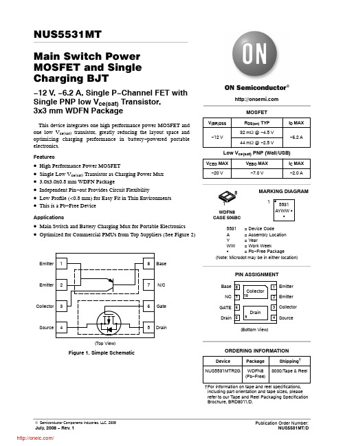
Emitter 1 Emitter 2 Collector 3 Source 4
t ≤ 10 s
TA = 25°C TA = 85°C TA = 25°C
TA = 25°C
VDSS VGS ID
PD
−12
V
±8.0
V
−5.47
A
−4.0
−6.2
1.46
W
2.1
Continuous Drain Current (Note 2)
Steady State TA = 25°C
ID
−4.4
(Note: Microdot may be in either location)
PIN ASSIGNMENT
Base 8 NC 7
Collector
10
GATE 6 Drain 5
Drain
9
1 Emitter 2 Emitter 3 Collector 4 Source
(Bottom View)
TL
260
°C
THERMAL RESISTANCE RATINGS
Parameter
Symbol
Max
Units
Junction−to−Ambient – Steady State (Note 3)
RqJA
299
°C/W
Junction−to−Ambient – t < 10 s (Note 3)
W25Q128JVSIQ规格书_W25Q128JVSIQ中文资料_W25Q128JVSIQ Datasheet
Publication Release Date: May 02, 2017Revision D3V 128M-BITSERIAL FLASH MEMORY WITH DUAL/QUAD SPI- 1 -Table of Contents1. GENERAL DESCRIPTIONS ............................................................................................................. 42. FEATURES ....................................................................................................................................... 43.PACKAGE TYPES AND PIN CONFIGURATIONS ........................................................................... 5 3.1 Pin Configuration SOIC 208-mil ........................................................................................... 5 3.2 Pad Configuration WSON 6x5-mm/ 8x6-mm ....................................................................... 5 3.3 Pin Description SOIC 208-mil, WSON 6x5-mm / 8x6-mm ................................................... 5 3.4 Pin Configuration SOIC 300-mil ........................................................................................... 6 3.5 Pin Description SOIC 300-mil ............................................................................................... 6 3.6 Ball Configuration TFBGA 8x6-mm (5x5 or 6x4 Ball Array) ................................................. 7 3.7Ball Description TFBGA 8x6-mm ......................................................................................... 7 4. PIN DESCRIPTIONS ........................................................................................................................ 8 4.1 Chip Select (/CS) .................................................................................................................. 8 4.2 Serial Data Input, Output and IOs (DI, DO and IO0, IO1, IO2, IO3) ..................................... 8 4.3 Write Protect (/WP) .............................................................................................................. 8 4.4 HOLD (/HOLD) ..................................................................................................................... 8 4.5 Serial Clock (CLK) ................................................................................................................ 8 4.6Reset (/RESET) (8)5. BLOCK DIAGRAM ............................................................................................................................ 96.FUNCTIONAL DESCRIPTIONS ..................................................................................................... 10 6.1 Standard SPI Instructions ................................................................................................... 10 6.2 Dual SPI Instructions .......................................................................................................... 10 6.3 Quad SPI Instructions ......................................................................................................... 10 6.4 Software Reset & Hardware /RESET pin ........................................................................... 10 6.5Write Protection (11)6.5.1 Write Protect Features (11)7. STATUS AND CONFIGURATION REGISTERS ............................................................................ 12 7.1Status Registers (12)7.1.1 Erase/Write In Progress (BUSY) – Status Only ................................................................ 12 7.1.2 Write Enable Latch (WEL) – Status Only .......................................................................... 12 7.1.3 Block Protect Bits (BP2, BP1, BP0) – Volatile/Non-Volatile Writable ................................ 12 7.1.4 Top/Bottom Block Protect (TB) – Volatile/Non-Volatile Writable ....................................... 13 7.1.5 Sector/Block Protect Bit (SEC) – Volatile/Non-Volatile Writable ....................................... 13 7.1.6 Complement Protect (CMP) – Volatile/Non-Volatile Writable ............................................ 13 7.1.1 Status Register Protect (SRP, SRL) – Volatile/Non-Volatile Writable ............................... 14 7.1.2 Erase/Program Suspend Status (SUS) – Status Only . (15)Publication Release Date: May 02, 2017- 2 - Revision D7.1.3 Security Register Lock Bits (LB3, LB2, LB1) – Volatile/Non-Volatile OTP Writable .......... 15 7.1.4 Quad Enable (QE) – Volatile/Non-Volatile Writable .......................................................... 15 7.1.5 Write Protect Selection (WPS) – Volatile/Non-Volatile Writable ....................................... 16 7.1.6 Output Driver Strength (DRV1, DRV0) – Volatile/Non-Volatile Writable ........................... 16 7.1.7 Reserved Bits – Non Functional ........................................................................................ 16 7.1.8 W25Q128JV Status Register Memory Protection (WPS = 0, CMP = 0) ............................... 17 7.1.9 W25Q128JV Status Register Memory Protection (WPS = 0, CMP = 1) ............................... 18 7.1.10 W25Q128JV Individual Block Memory Protection (WPS=1) . (19)8. INSTRUCTIONS ............................................................................................................................. 20 8.1Device ID and Instruction Set Tables (20)8.1.1 Manufacturer and Device Identification ................................................................................ 20 8.1.2 Instruction Set Table 1 (Standard SPI Instructions)(1)........................................................... 21 8.1.3 Instruction Set Table 2 (Dual/Quad SPI Instructions) ........................................................... 22 Notes: (22)8.2 Instruction Descriptions (23)8.2.1 Write Enable (06h) ............................................................................................................... 23 8.2.2 Write Enable for Volatile Status Register (50h) .................................................................... 23 8.2.3 Write Disable (04h) ............................................................................................................... 24 8.2.4 Read Status Register-1 (05h), Status Register-2 (35h) & Status Register-3 (15h) .............. 24 8.2.5 Write Status Register-1 (01h), Status Register-2 (31h) & Status Register-3 (11h) .............. 25 8.2.6 Read Data (03h) ................................................................................................................... 27 8.2.7 Fast Read (0Bh) ................................................................................................................... 28 8.2.8 Fast Read Dual Output (3Bh) ............................................................................................... 29 8.2.9 Fast Read Quad Output (6Bh) .............................................................................................. 30 8.2.10 Fast Read Dual I/O (BBh) ................................................................................................... 31 8.2.11 Fast Read Quad I/O (EBh) ................................................................................................. 32 8.2.12 Set Burst with Wrap (77h) .................................................................................................. 34 8.2.13 Page Program (02h) ........................................................................................................... 35 8.2.14 Quad Input Page Program (32h) ........................................................................................ 36 8.2.15 Sector Erase (20h) ............................................................................................................. 37 8.2.16 32KB Block Erase (52h) ..................................................................................................... 38 8.2.17 64KB Block Erase (D8h) ..................................................................................................... 39 8.2.18 Chip Erase (C7h / 60h) ....................................................................................................... 40 8.2.19 Erase / Program Suspend (75h) ......................................................................................... 41 8.2.20 Erase / Program Resume (7Ah) ......................................................................................... 42 8.2.21 Power-down (B9h) .............................................................................................................. 43 8.2.22 Release Power-down / Device ID (ABh) ............................................................................. 44 8.2.23 Read Manufacturer / Device ID (90h) ................................................................................. 45 8.2.24 Read Manufacturer / Device ID Dual I/O (92h) ................................................................... 46 8.2.25 Read Manufacturer / Device ID Quad I/O (94h) ................................................................. 47 8.2.26 Read Unique ID Number (4Bh). (48)- 3 -8.2.27 Read JEDEC ID (9Fh) ........................................................................................................ 49 8.2.28 Read SFDP Register (5Ah) ................................................................................................ 50 8.2.29 Erase Security Registers (44h) ........................................................................................... 51 8.2.30 Program Security Registers (42h) ...................................................................................... 52 8.2.31 Read Security Registers (48h) ........................................................................................... 53 8.2.32 Individual Block/Sector Lock (36h) ..................................................................................... 54 8.2.33 Individual Block/Sector Unlock (39h) .................................................................................. 55 8.2.34 Read Block/Sector Lock (3Dh) ........................................................................................... 56 8.2.35 Global Block/Sector Lock (7Eh) .......................................................................................... 57 8.2.36 Global Block/Sector Unlock (98h) ....................................................................................... 57 8.2.37 Enable Reset (66h) and Reset Device (99h) . (58)9.ELECTRICAL CHARACTERISTICS (59)9.1 Absolute Maximum Ratings (1) ............................................................................................ 59 9.2 Operating Ranges............................................................................................................... 59 9.3 Power-Up Power-Down Timing and Requirements ............................................................ 60 9.4 DC Electrical Characteristics- ............................................................................................. 61 9.5 AC Measurement Conditions .............................................................................................. 62 9.6 AC Electrical Characteristics (6) ........................................................................................... 63 9.7 Serial Output Timing ........................................................................................................... 65 9.8 Serial Input Timing .............................................................................................................. 65 9.9/WP Timing ......................................................................................................................... 65 10. PACKAGE SPECIFICATIONS ........................................................................................................ 66 10.1 8-Pin SOIC 208-mil (Package Code S) .............................................................................. 66 10.2 16-Pin SOIC 300-mil (Package Code F) ............................................................................ 67 10.3 8-Pad WSON 6x5-mm (Package Code P) ......................................................................... 68 10.4 8-Pad WSON 8x6-mm (Package Code E) ......................................................................... 69 10.5 24-Ball TFBGA 8x6-mm (Package Code B, 5x5-1 ball array) ............................................ 70 10.624-Ball TFBGA 8x6-mm (Package Code C, 6x4 ball array) ............................................... 71 11. ORDERING INFORMATION .......................................................................................................... 72 11.1Valid Part Numbers and Top Side Marking (73)12. REVISION HISTORY (74)Publication Release Date: May 02, 2017- 4 - Revision D1. GENERAL DESCRIPTIONSThe W25Q128JV (128M-bit) Serial Flash memory provides a storage solution for systems with limited space, pins and power. The 25Q series offers flexibility and performance well beyond ordinary Serial Flash devices. They are ideal for code shadowing to RAM, executing code directly from Dual/Quad SPI (XIP) and storing voice, text and data. The device operates on a single 2.7V to 3.6V power supply with current consumption as low as 1µA for power-down. All devices are offered in space-saving packages.The W25Q128JV array is organized into 65,536 programmable pages of 256-bytes each. Up to 256 bytes can be programmed at a time. Pages can be erased in groups of 16 (4KB sector erase), groups of 128 (32KB block erase), groups of 256 (64KB block erase) or the entire chip (chip erase). The W25Q128JV has 4,096 erasable sectors and 256 erasable blocks respectively. The small 4KB sectors allow for greater flexibility in applications that require data and parameter storage. (See Figure 2.)The W25Q128JV supports the standard Serial Peripheral Interface (SPI), Dual/Quad I/O SPI: Serial Clock, Chip Select, Serial Data I/O0 (DI), I/O1 (DO), I/O2 and I/O3. SPI clock frequencies of W25Q128JV of up to 133MHz are supported allowing equivalent clock rates of 266MHz (133MHz x 2) for Dual I/O and 532MHz (133MHz x 4) for Quad I/O when using the Fast Read Dual/Quad I/O. These transfer rates can outperform standard Asynchronous 8 and 16-bit Parallel Flash memories.Additionally, the device supports JEDEC standard manufacturer and device ID and SFDP, and a 64-bit Unique Serial Number and three 256-bytes Security Registers.2. FEATURES∙ New Family of SpiFlash Memories – W25Q128JV: 128M-bit / 16M-byte – Standard SPI: CLK, /CS, DI, DO – Dual SPI: CLK, /CS, IO 0, IO 1 – Quad SPI: CLK, /CS, IO 0, IO 1, IO 2, IO 3 – Software & Hardware Reset (1) ∙ Highest Performance Serial Flash – 133MHz Single, Dual/Quad SPI clocks – 266/532MHz equivalent Dual/Quad SPI – 66MB/S continuous data transfer rate – Min. 100K Program-Erase cycles per sector – More than 20-year data retention ∙ Efficient “Continuous Read”– Continuous Read with 8/16/32/64-Byte Wrap– As few as 8 clocks to address memory– Allows true XIP (execute in place) operation ∙ Low Power, Wide Temperature Range– Single 2.7 to 3.6V supply– <1µA Power-down (typ.)– -40°C to +85°C operating range∙ Flexible Architecture with 4KB sectors – Uniform Sector/Block Erase (4K/32K/64K-Byte) – Program 1 to 256 byte per programmable page – Erase/Program Suspend & Resume ∙ Advanced Security Features – Software and Hardware Write-Protect – Power Supply Lock-Down – Special OTP protection – Top/Bottom, Complement array protection – Individual Block/Sector array protection – 64-Bit Unique ID for each device – Discoverable Parameters (SFDP) Register– 3X256-Bytes Security Registers with OTP locks – Volatile & Non-volatile Status Register Bits ∙ Space Efficient Packaging – 8-pin SOIC 208-mil– 16-pin SOIC 300-mil (additional /RESET pin) – 8-pad WSON 6x5-mm / 8x6-mm – 24-ball TFBGA 8x6-mm (6x4/5x5 ball array) – Contact Winbond for KGD and other options Note: 1. Hardware /RESET pin is only available on TFBGA or SOIC16 packages- 5 -3. PACKAGE TYPES AND PIN CONFIGURATIONS3.1 Pin Configuration SOIC 208-milFigure 1a. W25Q128JV Pin Assignments, 8-pin SOIC 208-mil (Package Code S)3.2 Pad Configuration WSON 6x5-mm/ 8x6-mmFigure 1b. W25Q128JV Pad Assignments, 8-pad WSON 6x5-mm/ 8x6-mm (Package Code P/E)3.3 Pin Description SOIC 208-mil, WSON 6x5-mm / 8x6-mmNotes:1. IO0 and IO1 are used for Standard and Dual SPI instructions2.IO0 – IO3 are used for Quad SPI instructions, /HOLD (or /RESET) function is only available for Standard/Dual SPI.Publication Release Date: May 02, 2017- 6 - Revision D3.4 Pin Configuration SOIC 300-milFigure 1c. W25Q128JV Pin Assignments, 16-pin SOIC 300-mil (Package Code F)3.5 Pin Description SOIC 300-milNotes:1. IO0 and IO1 are used for Standard and Dual SPI instructions.2. IO0 – IO3 are used for Quad SPI instructions, /HOLD (or /RESET) function is only available for Standard/Dual SPI.3. The /RESET pin is a dedicated hardware reset pin regardless of device settings or operation states. If the hardware reset function is not used, this pin can be left floating or connected to VCC in the system.3.6Ball Configuration TFBGA 8x6-mm (5x5 or 6x4 Ball Array)Figure 1d. W25Q128JV Ball Assignments, 24-ball TFBGA 8x6-mm (Package Code B/C)3.7Ball Description TFBGA 8x6-mmNotes:1.IO0 and IO1 are used for Standard and Dual SPI instructions2.IO0 – IO3 are used for Quad SPI instructions, /HOLD (or /RESET) function is only available for Standard/Dual SPI.3. The /RESET pin is a dedicated hardware reset pin regardless of device settings or operation states.If the hardware reset function is not used, this pin can be left floating or connected to VCC in the system- 7 -Publication Release Date: May 02, 2017- 8 - Revision D4. PIN DESCRIPTIONS4.1 Chip Select (/CS)The SPI Chip Select (/CS) pin enables and disables device operation. When /CS is high the device is deselected and the Serial Data Output (DO, or IO0, IO1, IO2, IO3) pins are at high impedance. When deselected, the devices power consumption will be at standby levels unless an internal erase, program or write status register cycle is in progress. When /CS is brought low the device will be selected, power consumption will increase to active levels and instructions can be written to and data read from the device. After power-up, /CS must transition from high to low before a new instruction will be accepted. The /CS input must track the VCC supply level at power-up and power-down (see “Write Protection” and Figure 58). If needed a pull-up resister on the /CS pin can be used to accomplish this.4.2 Serial Data Input, Output and IOs (DI, DO and IO0, IO1, IO2, IO3)The W25Q128JV supports standard SPI, Dual SPI and Quad SPI operation. Standard SPI instructions use the unidirectional DI (input) pin to serially write instructions, addresses or data to the device on the rising edge of the Serial Clock (CLK) input pin. Standard SPI also uses the unidirectional DO (output) to read data or status from the device on the falling edge of CLK.Dual and Quad SPI instructions use the bidirectional IO pins to serially write instructions, addresses or data to the device on the rising edge of CLK and read data or status from the device on the falling edge of CLK. Quad SPI instructions require the non-volatile Quad Enable bit (QE) in Status Register-2 to be set. When QE=1, the /WP pin becomes IO2 and the /HOLD pin becomes IO3.4.3 Write Protect (/WP)The Write Protect (/WP) pin can be used to prevent the Status Register from being written. Used in conjunction with the Status Register’s Block Protect (CMP, SEC, TB, BP2, BP1 and BP0) bits and Status Register Protect (SRP) bits, a portion as small as a 4KB sector or the entire memory array can be hardware protected. The /WP pin is active low.4.4 HOLD (/HOLD)The /HOLD pin allows the device to be paused while it is actively selected. When /HOLD is brought low, while /CS is low, the DO pin will be at high impedance and signals on the DI and CLK pins will be ignored (don’t care). When /HOLD is brought high, device operation can resume. The /HOLD function can be useful when multiple devices are sharing the same SPI signals. The /HOLD pin is active low. When the QE bit of Status Register-2 is set for Quad I/O, the /HOLD pin function is not available since this pin is used for IO3. See Figure 1a-c for the pin configuration of Quad I/O operation.4.5 Serial Clock (CLK)The SPI Serial Clock Input (CLK) pin provides the timing for serial input and output operations. ("See SPI Operations")4.6 Reset (/RESET)A dedicated hardware /RESET pin is available on SOIC-16 and TFBGA packages. When it’s driven low for a minimum period of ~1µS, this device will terminate any external or internal operations and return to its power-on state.Note: Hardware /RESET pin is available on SOIC-16 or TFBGA; please contact Winbond for this package.- 9 -5. BLOCK DIAGRAMFigure 2. W25Q128JV Serial Flash Memory Block Diagram6.FUNCTIONAL DESCRIPTIONS6.1Standard SPI InstructionsThe W25Q128JV is accessed through an SPI compatible bus consisting of four signals: Serial Clock (CLK), Chip Select (/CS), Serial Data Input (DI) and Serial Data Output (DO). Standard SPI instructions use the DI input pin to serially write instructions, addresses or data to the device on the rising edge of CLK. The DO output pin is used to read data or status from the device on the falling edge of CLK.SPI bus operation Mode 0 (0,0) and 3 (1,1) are supported. The primary difference between Mode 0 and Mode 3 concerns the normal state of the CLK signal when the SPI bus master is in standby and data is not being transferred to the Serial Flash. For Mode 0, the CLK signal is normally low on the falling and rising edges of /CS. For Mode 3, the CLK signal is normally high on the falling and rising edges of /CS.6.2Dual SPI InstructionsThe W25Q128JV supports Dual SPI operation when using instructions such as “Fast Read Dual Output (3Bh)” and “Fast Read Dual I/O (BBh)”. These instructions allow data to be transferred to or from the device at two to three times the rate of ordinary Serial Flash devices. The Dual SPI Read instructions are ideal for quickly downloading code to RAM upon power-up (code-shadowing) or for executing non-speed-critical code directly from the SPI bus (XIP). When using Dual SPI instructions, the DI and DO pins become bidirectional I/O pins: IO0 and IO1.6.3Quad SPI InstructionsThe W25Q128JV supports Quad SPI operation when using instructions such as “Fast Read Quad Output (6Bh)”,and “Fast Read Quad I/O (EBh). These instructions allow data to be transferred to or from the device four to six times the rate of ordinary Serial Flash. When using Quad SPI instructions, the DI and DO pins become bidirectional IO0 and IO1, with the additional I/O pins: IO2, IO3.6.4Software Reset & Hardware /RESET pinThe W25Q128JV can be reset to the initial power-on state by a software Reset sequence. This sequence must include two consecutive instructions: Enable Reset (66h) & Reset (99h). If the instruction sequence is successfully accepted, the device will take approximately 30µS (t RST)to reset. No instruction will be accepted during the reset period. For the SOIC-16 and TFBGA packages, W25Q128JV provides a dedicated hardware /RESET pin. Drive the /RESET pin low for a minimum period of ~1µS (tRESET*) will interrupt any on-going external/internal operations and reset the device to its initial power-on state. Hardware /RESET pin has higher priority than other SPI input signals (/CS, CLK, IOs).Note:1.Hardware /RESET pin is available on SOIC-16 or TFBGA; please contact Winbond for his package.2.While a faster /RESET pulse (as short as a few hundred nanoseconds) will often reset the device, a 1us minimum isrecommended to ensure reliable operation.3.There is an internal pull-up resistor for the dedicated /RESET pin on the SOIC-16 and TFBGA-24 package. If the reset functionis not needed, this pin can be left floating in the system.6.5Write ProtectionApplications that use non-volatile memory must take into consideration the possibility of noise and other adverse system conditions that may compromise data integrity. To address this concern, the W25Q128JV provides several means to protect the data from inadvertent writes.6.5.1Write Protect Features∙Device resets when VCC is below threshold∙Time delay write disable after Power-up∙Write enable/disable instructions and automatic write disable after erase or program∙Software and Hardware (/WP pin) write protection using Status Registers∙Additional Individual Block/Sector Locks for array protection∙Write Protection using Power-down instruction∙Lock Down write protection for Status Register until the next power-up∙One Time Program (OTP) write protection for array and Security Registers using Status Register** Note:This feature is available upon special order. Please contact Winbond for details.Upon power-up or at power-down, the W25Q128JV will maintain a reset condition while VCC is below the threshold value of V WI, (See Power-up Timing and Voltage Levels and Figure 43). While reset, all operations are disabled and no instructions are recognized. During power-up and after the VCC voltage exceeds V WI, all program and erase related instructions are further disabled for a time delay of t PUW. This includes the Write Enable, Page Program, Sector Erase, Block Erase, Chip Erase and the Write Status Register instructions. Note that the chip select pin (/CS) must track the VCC supply level at power-up until the VCC-min level and t VSL time delay is reached, and it must also track the VCC supply level at power-down to prevent adverse command sequence. If needed a pull-up resister on /CS can be used to accomplish this.After power-up the device is automatically placed in a write-disabled state with the Status Register Write Enable Latch (WEL) set to a 0. A Write Enable instruction must be issued before a Page Program, Sector Erase, Block Erase, Chip Erase or Write Status Register instruction will be accepted. After completing a program, erase or write instruction the Write Enable Latch (WEL) is automatically cleared to a write-disabled state of 0.Software controlled write protection is facilitated using the Write Status Register instruction and setting the Status Register Protect (SRP, SRL) and Block Protect (CMP, TB, BP[3:0]) bits. These settings allow a portion or the entire memory array to be configured as read only. Used in conjunction with the Write Protect (/WP) pin, changes to the Status Register can be enabled or disabled under hardware control. See Status Register section for further information. Additionally, the Power-down instruction offers an extra level of write protection as all instructions are ignored except for the Release Power-down instruction.The W25Q128JV also provides another Write Protect method using the Individual Block Locks. Each 64KB block (except the top and bottom blocks, total of 126 blocks) and each 4KB sector within the top/bottom blocks (total of 32 sectors) are equipped with an Individual Block Lock bit. When the lock bit is 0, the corresponding sector or block can be erased or programmed; when the lock bit is set to 1, Erase or Program commands issued to the corresponding sector or block will be ignored. When the device is powered on, all Individual Block Lock bits will be 1, so the entire memory array is protected from Erase/Program. An “Individual Block Unlock (39h)” instruction must be issued to unlock any specific sector or block.The WPS bit in Status Register-3 is used to decide which Write Protect scheme should be used. When WPS=0 (factory default), the device will only utilize CMP, SEC, TB, BP[2:0] bits to protect specific areas of the array; when WPS=1, the device will utilize the Individual Block Locks for write protection.。
EMH11T2R;中文规格书,Datasheet资料
DatasheetEMH11 / UMH11N / IMH11ANPN 100mA 50V Complex Digital Transistors (Bias Resistor Built-in Transistors)l Features1) Built-In Biasing Resistors, R 1 = R 2 = 10k W .2) Two DTC114E chips in one package.3) Built-in bias resistors enable the configuration of an inverter circuit without connecting external input resistors (see inner circuit).4) The bias resistors consist of thin-film resistors with complete isolation to allow negative biasing l Inner circuitof the input. They also have the advantage of completely eliminating parasitic effects.5) Only the on/off conditions need to be set for operation, making the circuit design easy.6) Lead Free/RoHS Compliant.l ApplicationInverter circuit, Interface circuit, Driver circuitEMT6UMT6SMT63,000H11UMH11N UMT62021TR 1808SMT62928T10818088,000H118Tape width(mm)Basicorderingunit (pcs)Marking Reel size (mm)EMH11EMT61616T2R 1803,000H11IMH11APart No.Package Package size (mm)Taping code ParameterTr1 and Tr2V CC 50V I C(MAX.)100mA R 110k W R 210k WEMH11 (SC-107C)IMH11ASOT-457 (SC-74)UMH11N SOT-353 (SC-88)OUT (6)IN GND OUTIN (5)GND (4)OUT (4)IN GND OUTIN (5)GND (6)EMH11 / UMH11NIMH11A(6) (5) (4)(1) (2) (3)(4) (5) (6)(3) (2) (1)(6) (5) (4)(1) (2) (3)l Absolute maximum ratings (Ta = 25°C)l Electrical characteristics(Ta = 25°C)*2 Each terminal mounted on a reference footprint *3 120mW per element must not be exceeded.*4 200mW per element must not be exceeded.Fig.1 Input voltage vs. output current (ON characteristics) I N P U T V O L T A G E : V I (o n ) [V ]OUTPUT CURRENT : I O [A] Fig.2 Output current vs. input voltage (OFF characteristics)O U T P U T C U R R E N T : I O [A ]INPUT VOLTAGE : V I(off)[V]Fig.3 Output current vs. output voltageO U T P U T C U R R E N T : I O [m A ]OUTPUT VOLTAGE : V O [V] Fig.4 DC current gain vs. output currentD C C U R RE N T G A I N : G IOUTPUT CURRENT : I O [A]01020304050510Fig.5 Output voltage vs. output currentO U T P U T V O L T A G E : V O (o n ) [V ]OUTPUT CURRENT : I O[A]Dimension in mm/inchesEMT6Patterm of terminal position areasUMT6Patterm of terminal position areasSMT6Patterm of terminal position areasNoticeN o t e sNo copying or reprod uction of this d ocument, in part or in whole, is permitted without theconsent of ROHM Co.,Ltd.The content specified herein is subject to change for improvement without notice.The content specified herein is for the purpose of introd ucing ROHM's prod ucts (hereinafter"Products"). If you wish to use any such Product, please be sure to refer to the specifications,which can be obtained from ROHM upon request.Examples of application circuits, circuit constants and any other information contained hereinillustrate the standard usage and operations of the Products. The peripheral conditions mustbe taken into account when designing circuits for mass production.Great care was taken in ensuring the accuracy of the information specified in this document.However, should you incur any d amage arising from any inaccuracy or misprint of suchinformation, ROHM shall bear no responsibility for such damage.The technical information specified herein is intended only to show the typical functions of andexamples of application circuits for the Prod ucts. ROHM d oes not grant you, explicitly orimplicitly, any license to use or exercise intellectual property or other rights held by ROHM andother parties. ROHM shall bear no responsibility whatsoever for any dispute arising from theuse of such technical information.The Products specified in this document are intended to be used with general-use electronicequipment or devices (such as audio visual equipment, office-automation equipment, commu-nication devices, electronic appliances and amusement devices).The Products specified in this document are not designed to be radiation tolerant.While ROHM always makes efforts to enhance the quality and reliability of its Prod ucts, aProduct may fail or malfunction for a variety of reasons.Please be sure to implement in your equipment using the Products safety measures to guardagainst the possibility of physical injury, fire or any other damage caused in the event of thefailure of any Product, such as derating, redundancy, fire control and fail-safe designs. ROHMshall bear no responsibility whatsoever for your use of any Product outside of the prescribedscope or not in accordance with the instruction manual.The Products are not designed or manufactured to be used with any equipment, device orsystem which requires an extremely high level of reliability the failure or malfunction of whichmay result in a direct threat to human life or create a risk of human injury (such as a medicalinstrument, transportation equipment, aerospace machinery, nuclear-reactor controller, fuel-controller or other safety device). ROHM shall bear no responsibility in any way for use of anyof the Prod ucts for the above special purposes. If a Prod uct is intend ed to be used for anysuch special purpose, please contact a ROHM sales representative before purchasing.If you intend to export or ship overseas any Product or technology specified herein that maybe controlled under the Foreign Exchange and the Foreign Trade Law, you will be required toobtain a license or permit under the Law.Thank you for your accessing to ROHM product informations.More detail product informations and catalogs are available, please contact us.ROHM Customer Support System/contact/分销商库存信息: ROHMEMH11T2R。
US1中文资料
US1中文资料DISCRETE SEMICONDUCTORS DATA SHEETbook, halfpageM3D168US1 seriesSMA ultra fast low-losscontrolled avalanche rectifiersProduct speci?cation2000Feb14controlled avalanche recti?ersUS1 seriesFEATURESGlass passivatedHigh maximum operating temperatureIdeal for surface mount automotive applications ?Low leakage currentExcellent stabilityGuaranteed avalanche energy absorption capability ?UL94V-O classified plastic packageShipped in 12mm embossed tapeMarking: cathode, date code, type codeEasy pick and place.DESCRIPTIONDO-214AC surface mountable package with glass passivated chip.The well-defined void-free case is of a transfer-moulded thermo-setting plastic.The small rectangular package has two J bent leads.olumnsMSA474 Top view Side viewcathodebandk aFig.1 Simplified outline (DO-214AC) and symbol.LIMITING VALUESIn accordance with the Absolute Maximum Rating System (IEC134).SYMBOL PARAMETER CONDITIONS MIN.MAX.UNIT V RRM repetitive peak reverse voltageUS1A?50VUS1B?100VUS1D?200VUS1G?400VUS1J?600VV R continuous reverse voltageUS1A?50VUS1B?100VUS1D?200VUS1G?400VUS1J?600VV RMS root mean square voltageUS1A?35VUS1B?70VUS1D?140VUS1G?280VUS1J?420VI F(AV)average forward current averaged over any 20ms period;T tp=110°C; see Fig.21Acontrolled avalanche recti?ersUS1 seriesELECTRICAL CHARACTERISTICS T j =25°C unless otherwise speci?ed.THERMAL CHARACTERISTICS Notes1.Device mounted on Al 2O 3 printed-circuit board, 0.7mm thick; thickness of copper ≥35μm.2.Device mounted on epoxy-glass printed-circuit board, 1.5mm thick; thickness of copper ≥40μm. For moreinformation please refer to the ‘General Part of associated Handbook’.I FSMnon-repetitive peak forward currentt =8.3ms half sine wave;T j =25°C prior to surge;V R =V RRMmax ?25AT stg storage temperature ?65+175°C T jjunction temperatureSee Fig.365+175°CSYMBOL PARAMETER CONDITIONSTYP .MAX.UNITV Fforward voltage I F =1A;US1A to US1G see Fig.4? 1.1V US1J see Fig.51.4V I R reverse current V R =V RRMmax ; see Figs 6and 710μA V R =V RRMmax ; T j =165°C; see Figs 6and 7?50μA trr reverse recovery time when switched from I F =0.5A to I R =1A;measured at I R =0.25A; see Fig.12?50nsC ddiode capacitance V R =4V; f =1MHz;US1A to US1G see Fig.814?pF US1Jsee Fig.910pFSYMBOL PARAMETERCONDITIONSVALUE UNIT R th j-tp thermal resistance from junction to tie-point; see Fig.1027K/W R th j-a thermal resistance from junction to ambientnote 1100K/W note 2150K/WSYMBOL PARAMETERCONDITIONSMIN.MAX.UNITcontrolled avalanche recti?ersUS1 seriesGRAPHICAL DATAhandbook, halfpage 04020021.50.5180T tp (°C)I F(AV)(A)120160MCD822Fig.2Maximum permissible average forward current as a function of tie-pointtemperature (including losses due to reverse leakage).V R =V RRMmax ;δ=0.5; a =1.57.handbook, halfpage0100V R (%V Rmax )T j (°C)20010050MBK455Device mounted as shown in Fig.11.Solid line: Al 2O 3 printed-circuit board.Dotted line: epoxy printed-circuit board.Fig.3Maximum permissible junction temperature as a function of reverse voltage.handbook, halfpage32V F (V)I F(A)10MCD79210210110?110?210?3US1A to G T j =25°C.Fig.4Forward current as a function of forward voltage; typical values.handbook, halfpage42I F (A)V F (V)103MCD79310210110?110?210?3US1JT j =25°C.Fig.5Forward current as a function of forward voltage; typical values.controlled avalanche recti?ersUS1 serieshandbook, halfpage10002040V R (%V Rmax )I R (μA)608010210110?110?210?3MCD807T j = 165 °CT j = 25 °CFig.6Reverse current as a function of reverse voltage; typical values.US1A to Gf =1MHz; T j =25°C.handbook, halfpage10002040V R (%V Rmax )I R (μA)608010210110?110?210?3MCD806T j = 165 °CT j = 25 °CFig.7Reverse current as a function of reverse voltage; typical values.US1Jf =1MHz; T j =25°C.handbook, halfpage102101MCD79810?210?11V R (V)C d (pF)10102Fig.8Diode capacitance as a function of reverse voltage; typical values.US1 A to Gf =1MHz; T j =25°C.handbook, halfpage102101MCD79710?210?11V R (V)C d (pF)10102US1Jf =1MHz; T j =25°C.Fig.9Diode capacitance as a function of reverse voltage; typical values.controlled avalanche recti?ersUS1 serieshandbook, halfpage102101MBL120110Z th j-tp (K/W)102103t p (ms)104Fig.10Transient thermal impedance as a functionof pulse width.MSB2134.52.51.255050Fig.11 Printed-circuit board for surface mounting.Dimensions in mm.Material: Al 2O 3 or epoxy-glass.handbook, full pagewidth10 ?1 ?50 ?25 VDUT MAM057+t rr0.500.51.0I F (A)I R (A)t0.25Fig.12 Test circuit and reverse recovery time waveform and definition.Input impedance oscilloscope: 1M ?, 22pF; t r ≤7ns.Source impedance: 50?; t r ≤15ns.controlled avalanche recti?ersUS1 seriesPACKAGE OUTLINEREFERENCESOUTLINE VERSION EUROPEAN PROJECTIONISSUE DATE IECJEDEC EIAJSOD12499-10-22DO-214AC0 2.5 5 mmscaleTransfer-moulded thermo-setting plastic small rectangular surface mounted package;2 connectorsSOD124UNIT b A 1c D E Q mm1.61.40.20.052.82.44.54.3H 5.55.13.32.7DIMENSIONS (mm are the original dimensions)A 2.32.0DH AE b(1)A 1QcNote1. The marking band indicates the cathode.controlled avalanche recti?ersUS1 seriesDEFINITIONS LIFE SUPPORT APPLICATIONSThese products are not designed for use in life support appliances, devices, or systems where malfunction of these products can reasonably be expected to result in personal injury. Philips customers using or selling these products for use in such applications do so at their own risk and agree to fully indemnify Philips for any damages resulting from such improper use or sale.Data sheet status Objective speci?cation This data sheet contains target or goal speci?cations for product development.Preliminary speci?cation This data sheet contains preliminary data; supplementary data may be published later.Product speci?cation This data sheet contains ?nal product speci?cations.Limiting valuesLimiting values given are in accordance with the Absolute Maximum Rating System (IEC 60134).Stress above one or more of the limiting values may cause permanent damage to the device. These are stress ratings only and operation of the device at these or at any other conditions above those given in the Characteristics sections of the speci?cation is not implied. Exposure to limiting values for extended periods may affect device reliability.Application informationWhere application information is given, it is advisory and does not form part of the speci?cation.US1 series controlled avalanche recti?ersNOTESUS1 series controlled avalanche recti?ersNOTESUS1 series controlled avalanche recti?ersNOTESPhilips Electronics N.V.SCA All rights are reserved. Reproduction in whole or in part is prohibited without the prior written consent of the copyright owner.The information presented in this document does not form part of any quotation or contract,is believed to be accurate and reliable and may be changed without notice. No liability will be accepted by the publisher for any consequence of its use. Publication thereof does not convey nor imply any license under patent- or other industrial or intellectual property rights.Internet:/doc/2ec84a2e0722192e4536f6ec.html 200069Philips Semiconductors – a worldwide companyFor all other countries apply to: Philips Semiconductors,International Marketing &Sales Communications, Building BE-p, P.O.Box 218,5600MD EINDHOVEN, The Netherlands,Fax.+31402724825Argentina: see South America Australia: 3 Figtree Drive, HOMEBUSH, NSW 2140,Tel.+61297048141,Fax.+61297048139Austria:Computerstr. 6, A-1101 WIEN, P.O. Box 213,Tel.+431601011248, Fax.+431601011210Belarus: Hotel Minsk Business Center, Bld.3, r.1211, Volodarski Str.6,220050MINSK, Tel.+375172200733,Fax.+375172200773Belgium: see TheNetherlands Brazil:see South AmericaBulgaria:Philips Bulgaria Ltd., Energoproject, 15th floor,51James Bourchier Blvd., 1407SOFIA,T el.+3592689211,Fax.+3592689102Canada: PHILIPS SEMICONDUCTORS/COMPONENTS,T el.+18002347381,Fax.+18009430087China/Hong Kong: 501Hong Kong Industrial Technology Centre,72Tat Chee Avenue, Kowloon Tong, HONG KONG,Tel.+852********,Fax.+852********Colombia: see South America Czech Republic: see AustriaDenmark: Sydhavnsgade 23, 1780COPENHAGEN V,Tel.+4533293333,Fax.+4533293905Finland: Sinikalliontie 3, FIN-02630ESPOO,T el.+3589615800,Fax.+358961580920 France: 51Rue Carnot, BP317, 92156SURESNES Cedex,Tel.+33140996161,Fax.+33140996427Germany: Hammerbrookstra?e 69, D-20097HAMBURG,T el.+4940235360,Fax.+494023536300Hungary: see AustriaIndia: Philips INDIA Ltd, Band Box Building, 2nd floor,254-D,Dr.Annie Besant Road, Worli, MUMBAI 400025,Tel.+91224938541,Fax.+91224930966Indonesia:PT Philips Development Corporation,Semiconductors Division,Gedung Philips, Jl. Buncit Raya Kav.99-100, JAKARTA 12510,Tel.+62217940040ext.2501, Fax.+62217940080Ireland: Newstead, Clonskeagh, DUBLIN 14,Tel.+35317640000,Fax.+35317640200Israel: RAPAC Electronics, 7Kehilat Saloniki St, PO Box 18053,TEL AVIV 61180, Tel.+97236450444,Fax.+97236491007Italy:PHILIPS SEMICONDUCTORS,Via Casati,23-20052MONZA (MI),Tel. +390392036838,Fax +390392036800 Japan: Philips Bldg 13-37, Kohnan 2-chome, Minato-ku,TOKYO 108-8507, Tel.+81337405130,Fax.+81337405057Korea: Philips House, 260-199Itaewon-dong, Yongsan-ku, SEOUL,Tel.+8227091412,Fax.+8227091415Malaysia: No.76Jalan Universiti, 46200PETALING JAYA, SELANGOR,Tel.+60 37505214,Fax.+6037574880Mexico: 5900Gateway East, Suite 200, EL PASO, TEXAS 79905,Tel.+9-58002347381, Fax +9-58009430087Middle East: see ItalyNetherlands: Postbus 90050, 5600PB EINDHOVEN, Bldg.VB,Tel.+31402782785,Fax.+31402788399New Zealand: 2Wagener Place, C.P.O.Box 1041, AUCKLAND,Tel.+6498494160,Fax.+6498497811Norway: Box 1, Manglerud 0612, OSLO,Tel.+4722748000,Fax.+4722748341Pakistan: see Singapore Philippines: Philips Semiconductors Philippines Inc.,106Valero St.Salcedo Village, P.O.Box 2108MCC,MAKATI,Metro MANILA, Tel.+6328166380,Fax.+6328173474Poland : Al.Jerozolimskie 195B,02-222WARSAW,Tel.+48225710000,Fax.+48225710001Portugal: see Spain Romania: see ItalyRussia: Philips Russia, /doc/2ec84a2e0722192e4536f6ec.html atcheva 35A, 119048MOSCOW,Tel.+70957556918,Fax.+70957556919 Singapore: Lorong 1, Toa Payoh, SINGAPORE 319762,Tel.+653502538,Fax.+652516500Slovakia: see AustriaSlovenia: see ItalySouth Africa: S.A. PHILIPS Pty Ltd., 195-215Main Road Martindale,2092JOHANNESBURG, P.O.Box 58088 Newville 2114,Tel.+27114715401,Fax.+27114715398South America: Al.Vicente Pinzon,173, 6th floor,04547-130S?O PAULO,SP, Brazil,Tel.+55118212333,Fax.+55118212382Spain: Balmes 22, 08007BARCELONA,Tel.+34933016312,Fax.+34933014107 Sweden: Kottbygatan 7, Akalla, S-16485STOCKHOLM,Tel.+46859852000,Fax.+46859852745 Switzerland: Allmendstrasse 140, CH-8027ZüRICH,Tel.+4114882741Fax.+4114883263Taiwan: Philips Semiconductors, 6F, No.96, Chien Kuo N.Rd.,Sec.1,TAIPEI, Taiwan Tel.+886221342886,Fax.+886221342874Thailand: PHILIPS ELECTRONICS (THAILAND) Ltd.,209/2Sanpavuth-Bangna Road Prakanong, BANGKOK 10260,Tel.+6627454090,Fax.+6623980793Turkey: Yukari Dudullu, Org. San. Blg., 2.Cad. Nr. 28 81260Umraniye,ISTANBUL,Tel.+902165221500,Fax.+902165221813Ukraine : PHILIPS UKRAINE, 4Patrice Lumumba str., Building B, Floor 7,252042KIEV, Tel.+380442642776, Fax. +380442680461 United Kingdom: Philips Semiconductors Ltd., 276Bath Road, Hayes,MIDDLESEX UB35BX, Tel.+442087305000,Fax.+442087548421United States: 811East Arques Avenue, SUNNYVALE, CA 94088-3409,Tel.+18002347381, Fax.+18009430087Uruguay: see South AmericaVietnam: see SingaporeYugoslavia: PHILIPS, Trg N. Pasica 5/v,11000BEOGRAD,Tel.+381113341299,Fax.+381113342553 Printed in The Netherlands603502/250/01/pp 12 Date of release:2000Feb 14Document order number: 939775006784。
HSB857J中文资料
Page No. : 1/4HSB857JPNP EPITAXIAL PLANAR TRANSISTORDescriptionLow frequency power amplifier.Absolute Maximum Ratings (T A =25°C)• Maximum TemperaturesStorage Temperature............................................................................................................................. -50~+150 °C Junction Temperature................................................................................................................... +150 °C Maximum • Maximum Power DissipationTotal Power Dissipation (T C =25°C).....................................................................................................................20 W • Maximum Voltages and CurrentsBV CBO Collector to Base Voltage.........................................................................................................................-60 V BV CEO Collector to Emitter Voltage..................................................................................................................... -50 V BV EBO Emitter to Base Voltage............................................................................................................................. -5 V I C Collector Current.............................................................................................................................................. -3 A I C Collector Current (I C Peak)............................................................................................................................ -4.5 AElectrical Characteristics (T A =25°C)Symbol Min.Typ.Max.Unit Test ConditionsBV CBO -60--V I C =-50uA BV CEO -50--V I C =-1mA BV EBO -5--V I E=-50uA I CBO ---1uA V CB =-50V I CEO ---1uA V CE =-40V I EBO ---1uA V EB =-4V *V CE(sat)--0.3-1V I C =-2A, I B =-0.2A *V BE(sat)---1.5VI C =-2A, I B =-0.2A *h FE 170-400I C =-500mA, V CE =-3Vf T-15-MHz V CE =-5V, I C =-500mA, f=100MHz*Pulse Test: Pulse Width ≤380us, Duty Cycle ≤2%Page No. : 2/4Characteristics CurvePage No. : 3/4TO-252 DimensionImportant Notice:• All rights are reserved. Reproduction in whole or in part is prohibited without the prior written approval of HSMC.• HSMC reserves the right to make changes to its products without notice.• HSMC semiconductor products are not warranted to be suitable for use in Life-Support Applications, or systems.• HSMC assumes no liability for any consequence of customer product design, infringement of patents, or application assistance.Head Office And Factory:• Head Office (Hi-Sincerity Microelectronics Corp.): 10F.,No. 61, Sec. 2, Chung-Shan N. Rd. Taipei Taiwan R.O.C.Tel: 886-2-25212056 Fax: 886-2-25632712, 25368454• Factory 1: No. 38, Kuang Fu S. Rd., Fu-Kou Hsin-Chu Industrial Park Hsin-Chu Taiwan. R.O.C Tel: 886-3-5983621~5 Fax: 886-3-5982931Page No. : 4/4Soldering Methods for HSMC’s Products1. Storage environment: Temperature=10o C~35o C Humidity=65%±15%2. Reflow soldering of surface-mount devices Profile FeatureSn-Pb Eutectic AssemblyPb-Free AssemblyAverage ramp-up rate (T L to T P )<3o C/sec <3o C/sec Preheat- Temperature Min (Ts min )- Temperature Max (Ts max )- Time (min to max) (ts)100o C 150o C 60~120 sec 150o C 200o C 60~180 sec Tsmax to T L - Ramp-up Rate <3o C/sec <3o C/sec Time maintained above:- Temperature (T L )- Time (t L )183o C 60~150 sec 217o C 60~150 sec Peak Temperature (T P )240o C +0/-5o C 260o C +0/-5o C Time within 5o C of actual Peak Temperature (t P )10~30 sec 20~40 sec Ramp-down Rate<6o C/sec <6o C/sec Time 25o C to Peak Temperature <6 minutes<8 minutes3. Flow (wave) soldering (solder dipping)ProductsPeak temperature Dipping time Pb devices.245o C ±5o C 5sec ±1sec Pb-Free devices.260o C +0/-5o C5sec ±1sec。
- 1、下载文档前请自行甄别文档内容的完整性,平台不提供额外的编辑、内容补充、找答案等附加服务。
- 2、"仅部分预览"的文档,不可在线预览部分如存在完整性等问题,可反馈申请退款(可完整预览的文档不适用该条件!)。
- 3、如文档侵犯您的权益,请联系客服反馈,我们会尽快为您处理(人工客服工作时间:9:00-18:30)。
CS, INPUT pin, has 100k pull up. Negative edge will wake up the module and send the previous measured data first, after that temperature and humidity measurement will take place. As long as CS is low, measure<->send data cycle is repeated. 首先发送先前测到的数据,然后再开始温度 和湿度的测量。只要 CS 拉低,测量,发数 据的过程就会一直持续下去。 SDAT and SCK, OUTPUT pin, is in CMOS output mode. Thus for external MCU connection, ports connecting to this two pins should be in input mode without pull high resister to avoid high current. 因此,对于外部的 MCU 连接,端口应该设 定在输入模式,不带内部上拉电阻以避免额 外电流产生 2.2.1 CS CS is to activate the sensor and triggers to send out the previous measured temperature and humidity value through SCK and SDAT line. After data sent out, an internal AD convert cycle will start automatically. If CS line is kept low after AD convert, the new measured data will be output through the data lines until CS
Max 最大值
1
Repeatability 1
重复性
Accuracy
Temperature at
Uncertainty
0
0C – 50C range
精度不准确性
+,-3
+,-5
Interchangeability 互换性
Fully Inter Changeable
Nonlinearity 非线性
1
2
Figure 2: Reduce IO Usage Application
2.1 Power Pins The MTH01 sensor module requires a voltage supply between 2.0 to 5.5. After power, the sensor needs 20ms to complete its internal reset process. After reset finished, the sensor will make a measurement automatically and if the CS pin is low, then the measured data will be output automatically. MTH01 传感器模块需要 2.0 到 5.5 伏的电 压供应。上电后,传感器需要 20 豪秒时间 来完善其内部的重置过程。重置完成后,传 感器会自动测量,若 CS 脚被拉低,测量数 据会自动输出。 Power pins should be decoupled through a 10-100nF capacitor. Where in those applications with high power noise environment, it is strongly recommended to use a 10uF tantalum capacitor to protect the sensor from interferences. 需通过一个 10-100nF 的电容退耦。凡是在 高分贝噪音环境下的,强烈建议使用一个 10uf 钽电容,以保护传感器免被干扰。
MTH01-SPI
Temperature & Humidity Sensor
line goes high, which is to terminate the data output and AD convert process. When CS is high, the system enters sleep mode to reduce power consumption. 通过拉低 CS 就会立刻将上次测量数据发 送出来。数据发出后,一个将开始一个新温 度湿度数据的测量。如果测量完成后 CS 还 是低电平 ,新测量数据将会通过数据线输 出直到 CS 线变高为止,即数据输出和 AD 转换过程终止。当 CS 高时,系统进入睡眠 模式,以降低电力消耗。 2.2.2 SCK SCK is to synchronize the communication between MCU and the sensor module. It runs at around 2~3 KHZ speed, which should be an ideal speed for both high and low speed MCU systems. Once all data are out, SCK line will remain low. SCK 是使 MCU 和传感器模块间保持同步。 它以 3-6 千赫的速度运行,这应是高速和低 速单片机系统都理想的速度。一旦所有数据 都出来了,SCK 线将保持为低。
Temperature 温度
Resolution
0.1
Repeatability
0.1
0.2
Range
-40
70
Accuracy
25
+/-0.5
+/-1.0
Response Time
delta T=1.0
60
Unit 单位
% %
%
% % Second % %/yr
˚C ˚C ˚C ˚C
S
MTH01-SPI
2.2.3 SDAT SDAT is to transfer data to MCU. The SDAT line is valid after SCK goes high.
MTH01-SPI
Temperature & Humidity Sensor
- Relative humidity and temperature sensor - 相对温度和湿度传感器 - Pre-calculated temperature and humidity
read out, no extra calculation needed - 预先计算的温度和湿度读出,无需额外
Range
Temperature at
18
98
范围
0C – 50C range
Response Time
63% slowly
60
响应时间move air源自Hysterisis 重复性
Non-condensate 不结露
1
2
Long Term Stability 长期稳定性
Non-condensate
2
Product Summery 产品简介 The MTH01 is a MCU based temperature and relative humidity sensor module, comprising a SPI interface (master mode) for direct temperature and humidity read out. The digital output is pre-calculated and no extra calculation is required. The system applied two sensor elements: NTC type high precision temperature sensor and a resistor type relative humidity sensor from Japan. With a very unique and patented relative humidity calculation algorithm, the system can assure accurate relative humidity output through fine tuned
MTH01-SPI
Temperature & Humidity Sensor
Block Diagram
1. Module Performance Specification 模块性能规格
Parameter 参数
Resolution 分辨率
Conditions Min
条件
最小值 Typ
Humidity 湿度
Temperature & Humidity Sensor
2. Sensor Interface 传感器接口 Figure 1: Typical Application
2.2 Serial Interface 串行接口 The serial interface is optimized for convenient reading and reducing IO usage. Application engineer should be kept in mind the characteristics of the IO pins for applications where current consumption is critical. 串型接口是为方便读取和减少 IO 口用量 进行的优化设计。应用工程师应牢记 IO 口 的特性,对电流消耗有要求的场合是至关重 要的 Reset, INPUT pin, has 50k pull up resister connected internally, thus during normal application, the pin should not be tied to low unless reset is really needed.