(完整word版)Verilog-A30分钟快速入门教程.docx
verilog 教程

Verilog 的应用
Verilog HDL是一种用于数字逻辑电路设计的语言: - 用Verilog HDL描述的电路设计就是该电路
的 Verilog HDL模型。 - Verilog HDL 既是一种行为描述的语言也 是一种结构描述的语言。
这也就是说,既可以用电路的功能描述也可以用元器件和它们之间的连接来建立所设计电路的 Verilog HDL模型。Verilog模型可以是实际电路的不同级别的抽象。这些抽象的级别和它们 对应的模型类型共有以下五种:
state <= state <= state <= state <= 2 ’bxx;
Start; Stop; Clear; Idle;
设计示例四 (续)
always @(state or Reset or A) begin if ( !Reset) F = 0; else if (state == Stop) F = 1; end
设计示例一
• 用门级结构描述D触发器:
设计示例一 module input output nand #10 flop(data,clock,clear,q,qb); data,clock,clear; q,qb; nd1(a,data,clock,clear), nd2(b,ndata,clock), nd4(d,c,b,clear), nd5(e,c,nclock), nd6(f,d,nclock), nd8(qb,q,f,clear); nd3(c,a,d), nd7(q,e,qb); iv1(ndata,data), iv2(nclock,clock);
设计示例四 (续)
always @(posedge Clock) if (!Reset) begin state <= Idle; end else case (state) Idle: if (A) Start: if (!A) Stop: if (A) Clear: if (!A) default: state <= endcase
2024版华为Verilog入门教程

目录•Verilog概述•Verilog基础语法•组合逻辑电路设计•时序逻辑电路设计•数字系统设计方法学•华为Verilog编程规范与技巧Verilog概述1 2 3Verilog语言诞生,最初用于模拟电子系统的行为。
1980年代初期Verilog逐渐发展成为硬件描述语言(HDL),用于描述数字电路和系统的结构和行为。
1980年代中期Verilog不断完善和发展,成为电子设计自动化(EDA)领域的重要标准之一,广泛应用于集成电路设计、FPGA开发等领域。
1990年代至今Verilog历史与发展集成电路设计Verilog可用于描述数字集成电路的逻辑功能、时序关系和电路结构,是IC设计领域的重要工具。
FPGA开发Verilog可用于FPGA的逻辑设计和编程,实现复杂的数字系统和算法。
ASIC设计Verilog可用于ASIC设计的各个阶段,包括逻辑设计、综合、布局布线等。
系统级建模与仿真Verilog可用于构建系统级模型,进行系统仿真和性能分析。
Verilog应用领域01Verilog 是一种硬件描述语言(HDL ),用于描述数字电路和系统的结构和行为。
02与其他硬件描述语言(如VHDL )相比,Verilog具有更接近C 语言的语法风格,易于学习和使用。
Verilog 支持多种抽象层次的描述,包括行为级、寄存器传输级(RTL )、门级和开关级,方便设计师在不同设计阶段使用。
Verilog 与硬件描述语言关系02Verilog基础语法标识符与关键字标识符用于标识变量、模块、函数等程序实体的名称,由字母、数字和下划线组成,首字符必须是字母或下划线。
关键字Verilog语言中的保留字,用于定义语言结构和控制语句,如`module`、`input`、`output`、`if`、`else`等。
数据类型与运算符数据类型包括整型(`integer`)、实型(`real`)、时间型(`time`)以及用户自定义类型等。
Verilog教程

系统任务和系统函数在第 10章中详细讲解。
3.5 编译指令
以`(反引号)开始的某些标识符是编译器指令。在 Verilog 语言编译时,特定的编译器指 令在整个编译过程中有效(编译过程可跨越多个文件),直到遇到其它的不同编译程序指令。 完整的标准编译器指令如下 :
18 Verilog HDL 硬件描述语言
下载
3.5.7 `unconnected_drive和`nounconnected_drive
在模块实例化中,出现在这两个编译器指令间的任何未连接的输入端口或者为正偏电路 状态或者为反偏电路状态。
`unconnected_drive pull1 ... /*在这两个程序指令间的所有未连接的输入端口为正偏电路状态(连接到高电平) */ `nounconnected_drive
time_unit 和time_precision 由值1、10、和100以及单位s、ms、us、ns、ps和fs组成。例如:
`timescale 1ns/100ps
表示时延单位为 1ns, 时延精度为 100ps。`timescale 编译器指令在模块说明外部出现 , 并且影响 后面所有的时延值。例如 :
示十进制),h或H(表示十六进制)之一; value是基于 base的值的数字序列。值 x和z以及十
3.5.3 `default_nettype
该指令用于为隐式线网指定线网类型。也就是将那些没有被说明的连线定义线网类型。
`default_nettype wand
(完整word版)Verilog-A30分钟快速入门教程.docx
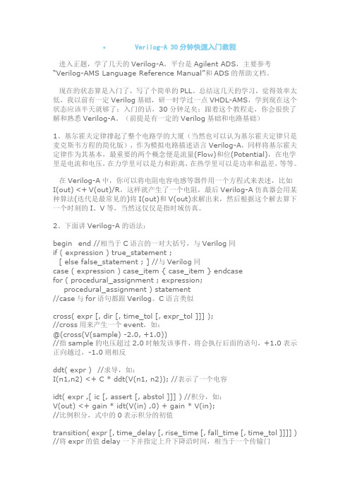
(完整word版)Verilog-A30分钟快速入门教程.docxVerilog-A 30分钟快速入门教程进入正题,学了几天的Verilog-A,平台是Agilent ADS,主要参考“ Verilog- AMS Language Reference Manual”和ADS的帮助文档。
现在的状态算是入门了,写了个简单的PLL。
总结这几天的学习,觉得效率太低,我以前有一定 Verilog 基础,研一时学过一点 VHDL-AMS ,学到现在这个状态应该半天就够了;入门的话, 30 分钟足矣;跟着这个教程走,你会很快了解和熟悉Verilog-A 。
(前提是有一定的Verilog 基础和电路基础)1、基尔霍夫定律撑起了整个电路学的大厦(当然也可以认为基尔霍夫定律只是麦克斯韦方程的简化版),作为模拟电路描述语言Verilog-A ,同样将基尔霍夫定律作为其基本,最重要的两个概念便是流量(Flow) 和位 (Potential) ,在电学里是电流和电压,在力学里可以是力和距离,在热学里可以是功率和温差,等等。
在Verilog-A中,你可以将电阻电容电感等器件用一个方程式来表述,比如I(out) <+ V(out)/R ,这样就产生了一个电阻,最后 Verilog-A 仿真器会用某种算法( 迭代是最常见的 ) 将 I(out) 和 V(out) 求解出来,然后根据这个解去算下一个时刻的 I 、V 等,当然这仅仅是指时域仿真。
2 、下面讲Verilog-A的语法:begin end //相当于C语言的一对大括号,与Verilog同if ( expression ) true_statement ;[ else false_statement ; ] //与Verilog同case ( expression ) case_item { case_item } endcasefor ( procedural_assignment ; expression;procedural_assignment ) statement//case与for语句都跟Verilog、C语言类似cross( expr [, dir [, time_tol [, expr_tol ]]] );//cross 用来产生一个 event ,如:@(cross(V(sample) -2.0, +1.0))//指 sample 的电压超过 2.0 时触发该事件,将会执行后面的语句,+1.0 表示正向越过, -1.0 则相反ddt( expr )// 求导,如:I(n1,n2) <+ C * ddt(V(n1, n2)); //表示了一个电容idt( expr ,[ ic [, assert [, abstol ]]] ) //积分,如:V(out) <+ gain * idt(V(in) ,0) + gain * V(in);// 比例积分,式中的 0 表示积分的初值transition( expr [, time_delay [, rise_time [, fall_time [, time_tol ]]]] )// 将 expr 的值 delay一下并指定上升下降沿时间,相当于一个传输门laplace_zp( expr ,ζ ,ρ)将expr 进行拉普拉斯变换,具体表达式参看相关文献,还有laplace_zd()等数据类型:integer 、real ,另外就是 discipline ,不知道怎么翻译比较好,比如说它将电压电流这两个nature 类型作为一个discipline ,这些都在disciplines.vams这个头文件里建好了,编程时要`include "disciplines.vams"。
(完整word版)Verilog-A30分钟快速入门教程
•Verilog-A 30分钟快速入门教程进入正题,学了几天的Verilog-A,平台是Agilent ADS,主要参考“Verilog-AMS Language Reference Manual”和ADS的帮助文档。
现在的状态算是入门了,写了个简单的PLL。
总结这几天的学习,觉得效率太低,我以前有一定Verilog基础,研一时学过一点VHDL-AMS,学到现在这个状态应该半天就够了;入门的话,30分钟足矣;跟着这个教程走,你会很快了解和熟悉Verilog-A。
(前提是有一定的Verilog基础和电路基础)1、基尔霍夫定律撑起了整个电路学的大厦(当然也可以认为基尔霍夫定律只是麦克斯韦方程的简化版),作为模拟电路描述语言Verilog-A,同样将基尔霍夫定律作为其基本,最重要的两个概念便是流量(Flow)和位(Potential),在电学里是电流和电压,在力学里可以是力和距离,在热学里可以是功率和温差,等等。
在Verilog-A中,你可以将电阻电容电感等器件用一个方程式来表述,比如I(out) <+ V(out)/R,这样就产生了一个电阻,最后Verilog-A仿真器会用某种算法(迭代是最常见的)将I(out)和V(out)求解出来,然后根据这个解去算下一个时刻的I、V等,当然这仅仅是指时域仿真。
2、下面讲Verilog-A的语法:begin end //相当于C语言的一对大括号,与Verilog同if ( expression ) true_statement ;[ else false_statement ; ] //与Verilog同case ( expression ) case_item { case_item } endcasefor ( procedural_assignment ; expression;procedural_assignment ) statement//case与for语句都跟Verilog、C语言类似cross( expr [, dir [, time_tol [, expr_tol ]]] );//cross用来产生一个event,如:@(cross(V(sample) -2.0, +1.0))//指sample的电压超过2.0时触发该事件,将会执行后面的语句,+1.0表示正向越过,-1.0则相反ddt( expr ) //求导,如:I(n1,n2) <+ C * ddt(V(n1, n2)); //表示了一个电容idt( expr ,[ ic [, assert [, abstol ]]] ) //积分,如:V(out) <+ gain * idt(V(in) ,0) + gain * V(in);//比例积分,式中的0表示积分的初值transition( expr [, time_delay [, rise_time [, fall_time [, time_tol ]]]] ) //将expr的值delay一下并指定上升下降沿时间,相当于一个传输门laplace_zp( expr ,ζ,ρ)将expr进行拉普拉斯变换,具体表达式参看相关文献,还有laplace_zd()等数据类型:integer、real,另外就是discipline,不知道怎么翻译比较好,比如说它将电压电流这两个nature类型作为一个discipline,这些都在disciplines.vams 这个头文件里建好了,编程时要`include "disciplines.vams"。
华为Verilog培训教程(2024)

工具链
Verilog工具链涵盖从设计 输入、模拟验证、综合到 最终硬件实现的整个过程 。
常用工具
常见的Verilog工具有 Cadence NC-Verilog、 ModelSim、Vivado等。
7
CHAPTER 02
Verilog语法与数据结构
2024/1/29
8
标识符、关键字和注释规范
2024/1/29
16
多路选择器、分配器实现策略
2024/1/29
多路选择器实现
根据选择信号从多个输入信号中选择一个输出。实现策略包括使用基本逻辑门搭 建、查找表方式实现等,可结合实际案例进行分析。
分配器实现
将单个输入信号分配到多个输出端上。实现策略包括使用数据分配器芯片、逻辑 门搭建等,可结合实际案例介绍分配器的工作原理及应用场景。同时,还可讨论 分配器在组合逻辑电路中的重要作用及其与其他逻辑器件的配合使用。
华为Verilog培训教程
2024/1/29
1
目录
2024/1/29
• Verilog概述与基础 • Verilog语法与数据结构 • 组合逻辑电路设计实例分析 • 时序逻辑电路设计实例分析 • 仿真测试与验证方法论述 • 模块化编程与IP封装技术探讨
2
CHAPTER 01
Verilog概述与基础
性能指标
包括处理速度、资源消耗、功 耗等方面的评估。
可靠性
评估IP核在长时间运行和极端 条件下的稳定性和可靠性。
功能正确性
评估IP核是否按照设计要求正 确实现功能。
2024/1/29
可重用性
评估IP核在不同应用场景下的 适应性和可配置性。
易用性
VerilogHDL入门(可编辑)

Verilog HDL入门Introduction to Verilog pldcomcnCourse Objectivesn Learn the basic constructs of Verilogn Learn the modeling structure of Verilogn Learn the concept of delays and their effects in simulationpldcomcnCourse OutlinenVerilog Overviewn Basic Structure of a Verilog Modeln Components of a Verilog Module– Ports– Data Types– Assigning Values and Numbers– Operators– Behavioral ModelingContinuous AssignmentsProcedural Blocks– Structural Modelingn Summary Verilog EnvironmentpldcomcnVerilogOverviewpldcomcnWhat is Verilogn IEEE industry standard Hardware DescriptionLanguage HDL - used to describe a digital system n For both Simulation SynthesispldcomcnVerilog Historyn Introduced in 1984 by Gateway Design Automationn 1989 Cadence purchased Gateway Verilog-XLsimulatorn 1990 Cadence released Verilog to the publicn Open Verilog International OVI was formed to control the language specificationsn 1993 OVI released version 20n 1993 IEEE accepted OVI Verilog as a standard Verilog 1364pldcomcnVerilog StructurenVerilog HDL Consists of Keywords syntax andsemantics used to describe hardware functionality and timingn PLI Programming Language Interface provides Clanguage routines used to interact between Verilog and EDA tools SimulatorsWaveform displaysn SDF Standard Delay Format - a file used to back-annotate accurate timing information to simulators and other toolspldcomcnTerminologyn HDL - Hardware Description Language is a softwareprogramming language that is used to model a piece of hardwaren Behavior Modeling - A component is described by itsinputoutput responsen Structural Modeling - A component is described byinterconnecting lower-level componentsprimitives pldcomcnBehavior Modelingn Only the functionality of the circuit no structure n No specific hardware intentn For the purpose of synthesis as well as simulationoutput 1 outputninput 1 inputnif input 1for j 0 j 8 j j25 output 1 1b0elsefor j 1 j 8 j j25 output 1 1b1pldcomcnStructural Modelingn Functionality and structure of the circuitn Call out the specific hardwaren For the purpose of synthesisHigher-level Componentinput1 output 1Lower-levelComponent1Lower-levelComponent1inputnoutputnpldcomcnMore Terminologyn Register Transfer Level RTL - A type of behavioralmodeling for the purpose of synthesis– Hardware is implied or inferred– Synthesizablen Synthesis - Translating HDL to a circuit and thenoptimizing the represented circuitn RTL Synthesis - The process of translating a RTLmodel of hardware into an optimized technologyspecific gate level implementationpldcomcnRTL Synthesisalways a or b or c or d or sel ainferredbegin b mux_outcase sel c2b00 mux_out a d2b01 mux_out b sel2b10 mux_out c 22b11 mux_out dendcaseaTranslationdaOptimization dpldcomcnVerilog vs Other HDL StandardsnVerilog– Tell me how your circuit should behave and I will give youthe hardware that does the jobnVHDL– Similar to VerilognABEL PALASM AHDL– Tell me what hardware you want and I will give it to youpldcomcnVerilog vs Other HDL StandardsnVerilog– Give me a circuit whose output only changes when there isa low-to-high transition on a particular input When thetransition happens make the output equal to the input untilthe next transition–Result Verilog Synthesis provides a positive edge-triggeredflipflopnABEL PALASM AHDL– Give me a D-type flipflop– Result ABEL PALASM AHDL synthesis provides a D-typeflipflop The sense of the clock depends on the synthesistoolpldcomcnTypical Synthesis Design FlowVerilog TechnologyModel LibrarySynthesisCompilerTiming Analysis Netlist PlaceRouteText OutputTestSimulationVectorsWaveformpldcomcnTypical Simulation Design FlowVerilog VerilogModelTestBenchOptionalSimulationCompilerSimulation TestModel VectorsWaveform Verilog Text OutputSimulationpldcomcnVerilogModelingpldcomcnVerilog - Basic Modeling Structuren CASE-sensitvemodule module_name port_list nAll keywords areport declarations lowercasenWhitespace is used fordata type declarations readabilitynSemicolon is thecircuit functionality statement terminatornSingle line commenttiming specifications n Multi-line commentendmodule nTiming specification isfor simulationpldcomcnComponents of a Verilog ModulemoduleTiming SpecificationsPort ListPort Data Type Circuit SubprogramsDeclarations Declarations FunctionalityInstantiation taskinput NetContinuous Procedural functionoutput Register Assignment BlocksSystem Tasksinout parameter assign initialblockCompilerDirectivesalwaysblockpldcomcnComponents of a Verilog Modulemodule Module_name Port_listPort declarations if ports are presentParameters optionalData type declarationsContinuous Assignments assignProcedural Blocks initial andalways- behavioral statementsInstantiation of lower-level modulesTasks and FunctionsTiming SpecificationsendmodulepldcomcnSchematic Representation - MACadder_outoutinaD Qmult_out clkXinbclr CLRNpldcomcnVerilog Model Mulitiplier-Accumulator MACtimescale 1 ns 10 ps assign adder_out mult_out outmodule mult_acc out ina inb clk clr alwaysposedge clk or posedge clrbegininput [70] ina inb if clrinput clk clr out 16h0000output [150] out elseout adder_outwire [150] mult_out adder_out endreg [150] outmulta u1 in_a ina in_b inb m_out mult_outparameter set 10parameter hld 20 specify setup ina posedge clk sethold posedge clk ina hldsetup inb posedge clk sethold posedge clk inb hldendspecifyendmodulepldcomcnLets take a look atmoduleTiming SpecificationsPort ListPort Data Type Circuit SubprogramsDeclarations Declarations FunctionalityInstantiation taskinput NetContinuous Procedural functionoutput Register Assignment BlocksSystem Tasksinout parameter assign initialblock CompilerDirectivesalwaysblockpldcomcnPortsn Port List– A listing of the port names– Examplemodule mult_acc out ina inb clk clr n Port Types– input -- input port– output -- output port– inout -- bidirectional portn Port Declarations–– Exampleinput [70] ina inbinput clk clroutput [150] outpldcomcnPorts List and Declarationtimescale 1 ns 10 ps assign adder_out mult_out outmodule mult_acc out ina inb clk clr always posedge clk or posedge clrbegininput [70] ina inb if clrout 16h0000input clk clr elseoutput [150] out out adder_outendwire [150] mult_out adder_outreg [150] out multa u1 in_aina in_b inb m_out mult_outparameter set 10 specifyparameter hld 20 setup ina posedge clk sethold posedge clk ina hldsetup inb posedge clk sethold posedge clk inb hldendspecify endmodule pldcomcnData Typesn Net Data Type - represent physical interconnect betweenprocesses activity flowsprocess processFunctional Functionalnets nets nets Block BlockMUX Addersnets netsnRegister Data Type - represent variable to store datatemporarily– It does not represent a physical hardware registerTemporary StoragepldcomcnNet Data Typenwire -- represents a nodentri -- represents a tri-state node n Bus Declarations– [MSB LSB ]– [LSB MSB]n Examples– wire– wire [150] mult_out adder_outpldcomcnNet Data TypesSupported byNet Data Type Functionality Synthesiswire tri Used for interconnectsupply0 supply1 Constant logic valuewand triand Used to model ECLwor trior Used to model ECLtri0 tri1 Pull-down Pull-uptrireg Stores last value whennot drivenpldcomcnRegister Data Typesnreg - unsigned variable of any bit size ninteger - signed variable usually 32 bits n Bus Declarations– [MSB LSB ]– [LSB MSB]n Examples– reg– reg [7 0] outpldcomcnRegister Data TypesRegisterSupported byData Type Functionality Synthesisreg Unsigned variable ofany bit sizeinteger Signed variable -usually 32 bitstime Unsigned integer -usually 64 bitsreal Double precisionfloating point variablepldcomcnMemorynTwo dimensional register arrayn Can not be a net typen Examplesreg [310] mem[01023] 1Kx32 reg [310] instrinstr mem[2]n Double-indexing is not permittedinstr mem[2][70] Illegal pldcomcnParametern Parameter - assigning a value to a symbolic nameparameter size 8reg [size-10] a bpldcomcnData Typen Every signal which includes ports must have a datatype– Signals must be explicitly declared in the data type declarations of your module– Ports are by default wire net data types if theyare not explicitly declaredpldcomcnData Types Declarationtimescale 1 ns 10 ps assignadder_out mult_out outmodule mult_acc out ina inb clk clr alwaysposedge clk or posedge clrbegininput [70] ina inb if clrinput clk clr out 16h0000output [150] out elseout adder_outwire [150] mult_out adder_out endreg [150] out multa u1 in_aina in_b inb m_out mult_outparameter set 10 specifyparameter hld 20 setup ina posedge clk sethold posedge clk ina hldsetup inb posedge clk sethold posedge clk inb hldendspecifyendmodule pldcomcnAssigning Values - NumbersandOperatorspldcomcnAssigning Values - NumbersnAre sized or unsized– Sized example 3b010 3-bit wide binary number The prefix 3 indicates the size of number– Unsized example 123 32-bit wide decimal number by defaultDefaults– No specified defaults to decimal–No specified defaults to 32-bit wide numbern Base Format–Decimal d or D 16d255 16-bit wide decimal number– Hexadecimal h or H 8h9a 8-bit wide hexadecimal number– Binary b or B b1010 32-bit wide binary numer– Octal o or O o21 32-bit wide octal numberpldcomcnNumbersn Negative numbers - specified by putting a minus sign beforethe– Legal -8d3 8-bit negative number stored as 2s complement of 3– Illegal 4d-2 ERRORn Special Number Characters– _ underscore used for readabilityExample 32h21_65_bc_fe 32-bit hexadecimal number– x or X unknown valueExample 12h12x 12-bit hexadecimal number LSBs unknown– z or Z high impedance valueExample 1bz 1-bit high impedance numberpldcomcnNumbersn Extended– If MSB is 0 x or z number is extended to fill MSBs with 0 xorz respectivelyExamples 3b01 3b001 3bx1 3bxx1 3bz 3bzzz– If MSB is 1 number is extended to fill MSBs with 0Example 3b1 3b001pldcomcnShort Quizn Short Quiz– Q What is the actual value for 4d017 in binary pldcomcnAnswersn Short Quiz– Q What is the actual value for 4d017 in binary– A 4b0001 MSB is truncated 10001pldcomcnArithmetic OperatorsOperator Operation ExamplesSymbol Performed ain 5 bin 10 cin 2b01 din 2b0ZAdd bin cin 11- Subtract Negate bin - cin 9 -bin -10Multiply ain bin 50Divide bin ain 2Modulus bin ain 0nTreats vectors as a whole valuen If any operand is Z or X then the results are unknown– Example ain din unknownn If results and operands are same size then carry is lostpldcomcnBitwise OperatorsOperator Operation ExamplesSymbol Performed ain 3b101 bin 3b110 cin 3b01XInvert each bit ain is 3b010And each bit ain bin is 3 b100 bin cin is 3b010Or each bit ain bin is 3b111Xor each bit ain bin is 3 b011or Xnor each bit ain bin 3b100n Operates on each bit of the operandn Result is the size of the largest operandn Left-extended if sizes are differentpldcomcnReduction OperatorsOperator Operation ExamplesSymbol Performed ain 5b10101 bin 4b0011cin 3bZ00 din 3bX011And all bits ain 1b0 din 1b0Nand all bits ain 1b1Or all bits ain 1b1 cin 1bXNor all bits ain 1b0Xor all bits ain 1b1or Xnor all bits ain 1b0n Reduces a vector to a single bitnX or Z are considered unkown but result maybe a knownvalue– Example din results in 1b0pldcomcnRelational OperatorsOperator Operation ExamplesSymbol Performed ain 3b010 bin 3b100 cin 3b111。
verilog教程

verilog教程当您开始学习Verilog时,以下是一些重要的基础知识和概念。
1. Verilog是一种硬件描述语言(HDL),用于描述和设计数字电路。
它可以用于模拟、合成和验证电路。
2. Verilog使用模块化的设计风格。
每个设计都由一个或多个模块组成,每个模块有自己的输入和输出。
3. 使用`module`关键字定义一个模块,并在其后给出模块的名称。
```verilogmodule my_module;// 模块主体endmodule```4. 模块内部包含用`input`和`output`声明的端口,用于与其他模块进行通信。
```verilogmodule my_module(input wire a,input wire b,output wire c);// 模块主体endmodule```5. `wire`关键字用于声明连接不同模块的导线。
可以将导线看作是用于传输数字信号的线。
6. 在模块主体中,可以使用`assign`关键字创建逻辑连接。
逻辑连接使用`=`运算符连接输入和输出。
```verilogmodule my_module(input wire a,input wire b,output wire c);assign c = a & b;endmodule```7. 除了逻辑连接外,可以在模块内部使用`always`块创建组合和时序逻辑。
```verilogmodule my_module(input wire a,input wire b,output wire c);reg d;always @(a or b)d = a | b;assign c = d;endmodule```8. Verilog还支持使用`if-else`语句,`case`语句和循环结构等常见的编程结构。
9. 为了模拟和验证设计,可以使用Verilog仿真工具,如ModelSim、VCS等。
- 1、下载文档前请自行甄别文档内容的完整性,平台不提供额外的编辑、内容补充、找答案等附加服务。
- 2、"仅部分预览"的文档,不可在线预览部分如存在完整性等问题,可反馈申请退款(可完整预览的文档不适用该条件!)。
- 3、如文档侵犯您的权益,请联系客服反馈,我们会尽快为您处理(人工客服工作时间:9:00-18:30)。
?Verilog-A 30分钟快速入门教程
进入正题,学了几天的Verilog-A,平台是Agilent ADS,主要参考
“ Verilog- AMS Language Reference Manual”和ADS的帮助文档。
现在的状态算是入门了,写了个简单的PLL。
总结这几天的学习,觉得效率太低,我以前有一定 Verilog 基础,研一时学过一点 VHDL-AMS ,学到现在这个状态应该
半天就够了;入门的话, 30 分钟足矣;跟着这个教程走,你会很快了解和熟悉Verilog-A 。
(前提是有一定的 Verilog 基础和电路基础)
1、基尔霍夫定律撑起了整个电路学的大厦(当然也可以认为基尔霍夫定律只是
麦克斯韦方程的简化版),作为模拟电路描述语言 Verilog-A ,同样将基尔霍夫定律作为其基本,最重要的两个概念便是流量 (Flow) 和位 (Potential) ,在电学里是电流
和电压,在力学里可以是力和距离,在热学里可以是功率和温差,等等。
在 Verilog-A中,你可以将电阻电容电感等器件用一个方程式来表述,比如
I(out) <+ V(out)/R ,这样就产生了一个电阻,最后 Verilog-A 仿真器会用某种算法( 迭代是最常见的 ) 将 I(out) 和 V(out) 求解出来,然后根据这个解去算下一个时刻
的 I 、V 等,当然这仅仅是指时域仿真。
2 、下面讲Verilog-A的语法:
begin end //相当于C语言的一对大括号,与Verilog
同
if ( expression ) true_statement ;
[ else false_statement ; ] //与Verilog同
case ( expression ) case_item { case_item } endcase
for ( procedural_assignment ; expression;
procedural_assignment ) statement
//case与for语句都跟Verilog、C语言类似
cross( expr [, dir [, time_tol [, expr_tol ]]] );
//cross 用来产生一个 event ,如:
@(cross(V(sample) -2.0, +1.0))
//指 sample 的电压超过 2.0 时触发该事件,将会执行后面的语句, +1.0 表示正向
越过, -1.0 则相反
ddt( expr )// 求导,如:
I(n1,n2) <+ C * ddt(V(n1, n2)); //表示了一个电容
idt( expr ,[ ic [, assert [, abstol ]]] ) //积分,如:
V(out) <+ gain * idt(V(in) ,0) + gain * V(in);
// 比例积分,式中的 0 表示积分的初值
transition( expr [, time_delay [, rise_time [, fall_time [, time_tol ]]]] )
// 将 expr 的值 delay一下并指定上升下降沿时间,相当于一个传输门
laplace_zp( expr ,ζ ,ρ)
将 expr 进行拉普拉斯变换,具体表达式参看相关文献,还有laplace_zd()等
数据类型:
integer 、real ,另外就是 discipline ,不知道怎么翻译比较好,比如说它将电压
电流这两个 nature 类型作为一个 discipline ,这些都在 disciplines.vams
这个头文件里建好了,编程时要`include "disciplines.vams"。
如果要定义一个电路节点, electrical node_name就好了
parameter {real | integer} list_of_assignments ;
// 定义参数,如 parameter R = 50 from (0:inf];
在一个模块中调另一个模块和Verilog差不多,如:
blk_a a1(Input1, a_b1);
blk_a a2(Input2, a_b2);
运算符号:
+ - * / > < == & | && || ^ << >> ?:等,跟Verilog一样
另外,新加的一个符号 <+ ,这个专门给模拟信号赋值用,注意这个赋值符号是
可以累加的,就是说赋两次值的话,它会加起来,而不是覆盖,如:
// model input admittance(导纳)
I(in) <+ V(in)/Rin;
I(in) <+ Cin*ddt(V(in));
预处理 & 宏:
`define`else`ifdef`include`resetall`undef
跟 Verilog 差不多
3 、Verilog-A程序基本结构:
`include "disciplines.vams"// 预处理
module load(p);// 定义模块, p 是端口
electrical p, gnd;// 定义节点
ground gnd;// 定义 gnd 为 ground节点,电位为0
parameter real R=50.0;// 定义 R 这个参数并赋初值
analog// 模拟语句从这开始
V(p) <+ R * I(p, gnd);// 在这里表示一个电阻,表示了输出电压与输出电流的关系
endmodule// 模块定义结束
4 、上面这些基本上是最常用的了,了解之后,你就能看懂一般的Verilog-A 程序了,下面是我写的PLL 仿真程序,把它看完并看懂(当然第一次并不需要看得很仔细):
提示:振荡频率 4~6G ,分频器为 50 分频,Fref 为 100M ,鉴相器为电荷泵型。
`include "disciplines.vams"
`include "constants.vams"
//VCO
module my_vco(in, out);
input in;
output out;
electrical in, out;
parameter real gain=2.0e9, fc=4.0e9;
analog
V(out) <+ sin(2*`M_PI*(fc*$realtime + idt(gain*V(in))));
endmodule
//phase detector
module my_pd(ref,rf,outP,outN);
input ref,rf;
output outP,outN;
electrical ref,rf,outP,outN;
real clr,up,down;
parameter real Ro=1e6, Ro2=1;
analog begin
@(cross(V(ref)-0.5,+1))
up = 1;
@(cross(V(rf)-0.5,+1))
down = 1;
clr = absdelay(up && down, 1e-9);
// clr = transition(up && down, 1e-9); // 这两条语句都可以 if(clr>0.5) begin
up = 0;
down = 0;
end
if(up) begin
if(V(outP)>= 3)
V(outP) <+ 3-I(outP)*Ro2;
else I(outP) <+ -up*0.01;
end
else begin
I(outP) <+ 0;
end
if(down) begin
if(V(outN) <= 0)
V(outN) <+ 0-I(outN)*Ro2;
else I(outN) <+ down*0.01;
end
else begin
I(outN) <+ 0;
end
end
endmodule
//N divider
module my_divider(in,out);
input in;
output out;
electrical in,out;
integer cnt;
parameter integer K=50;
analog begin
@(cross(V(in),+1))
cnt = cnt+1;
if(cnt>=K)
cnt=0;
if(cnt*2-K>=0)
V(out) <+ 1;
else
V(out) <+ 0;
end
endmodule
以上是 VCO 、鉴相器和分频器,原理图我是在ADS 中画的,如下所示:
以下是仿真结果:
好,看到这儿你已经入门了,想进一步熟悉Verilog-A的话,请参看:。