Superconducting Gap Structure of kappa-(BEDT-TTF)2Cu(NCS)2 Probed by Thermal Conductivity T
Zero-gap materials零能隙材料
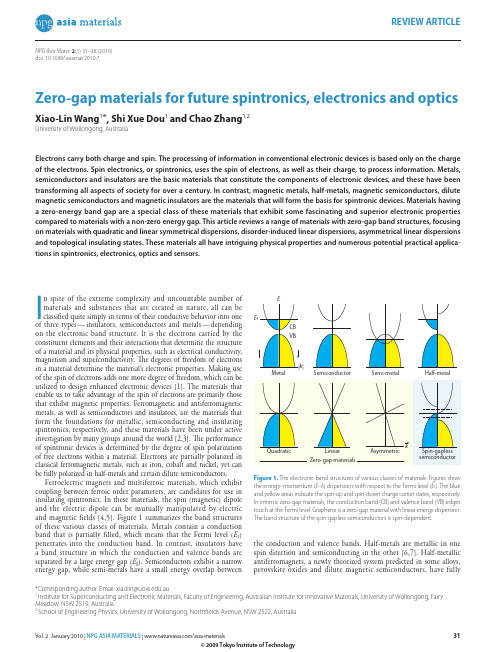
REVIEW ARTICLENPG Asia Mater. 2(1) 31–38 (2010)doi: 10.1038/asiamat.2010.7In spite of the extreme complexity and uncountable number of materials and substances that are created in nature, all can be classifi ed quite simply in terms of their conductive behavior into one of three types — insulators, semiconductors and metals — depending on the electronic band structure. It is the electrons carried by the constituent elements and their interactions that determine the structure of a material and its physical properties, such as electrical conductivity, magnetism and superconductivity. Th e degrees of freedom of electrons in a material determine the material’s electronic properties. Making use of the spin of electrons adds one more degree of freedom, which can be utilized to design enhanced electronic devices [1]. The materials that enable us to take advantage of the spin of electrons are primarily those that exhibit magnetic properties. Ferromagnetic and antiferromagnetic metals, as well as semiconductors and insulators, are the materials that form the foundations for metallic, semiconducting and insulating spintronics, respectively, and these materials have been under active investigation by many groups around the world [2,3]. Th e performance of spintronic devices is determined by the degree of spin polarization of free electrons within a material. Electrons are partially polarized in classical ferromagnetic metals, such as iron, cobalt and nickel, yet can be fully polarized in half-metals and certain dilute semiconductors.Ferroelectric magnets and multiferroic materials, which exhibit coupling between ferroic order parameters, are candidates for use in insulating spintronics. In these materials, the spin (magnetic) dipole and the electric dipole can be mutually manipulated by electric and magnetic fields [4,5]. Figure 1 summarizes the band structures of these various classes of materials. Metals contain a conduction band that is partially filled, which means that the Fermi level (E f ) penetrates into the conduction band. In contrast, insulators have a band structure in which the conduction and valence bands are separated by a large energy gap (E g ). Semiconductors exhibit a narrow energy gap, while semi-metals have a small energy overlap betweenthe conduction and valence bands. Half-metals are metallic in one spin direction and semiconducting in the other [6,7]. Half-metallic antiferromagnets, a newly theorized system predicted in some alloys, perovskite oxides and dilute magnetic semiconductors, have fullyZero-gap materials for future spintronics, electronics and opticsXiao-Lin Wang 1*, Shi Xue Dou 1 and Chao Zhang 1,2University of Wollongong, AustraliaElectrons carry both charge and spin. The processing of information in conventional electronic devices is based only on the charge of the electrons. Spin electronics, or spintronics, uses the spin of electrons, as well as their charge, to process information. Metals, semiconductors and insulators are the basic materials that constitute the components of electronic devices, and these have been transforming all aspects of society for over a century. In contrast, magnetic metals, half-metals, magnetic semiconductors, dilute magnetic semiconductors and magnetic insulators are the materials that will form the basis for spintronic devices. Materials having a zero-energy band gap are a special class of these materials that exhibit some fascinating and superior electronic properties compared to materials with a non-zero energy gap. This article reviews a range of materials with zero-gap band structures, focusing on materials with quadratic and linear symmetrical dispersions, disorder-induced linear dispersions, asymmetrical linear dispersions and topological insulating states. These materials all have intriguing physical properties and numerous potential practical applica-tions in spintronics, electronics, optics and sensors.*Corresponding author. Email: xiaolin@.au 1Institute for Superconducting and Electronic Materials, Faculty of Engineering, Australian Institute for Innovative Materials, University of Wollongong, Fairy Meadow, NSW 2519, Australia 2School of Engineering Physics, University of Wollongong, Northfi elds Avenue, NSW 2522, AustraliaFigure 1. The electronic band structures of various classes of materials. Figures show the energy–momentum (E –k ) dispersions with respect to the Fermi level (E f ). The blue and yellow areas indicate the spin-up and spin-down charge carrier states, respectively. In intrinsic zero-gap materials, the conduction band (CB) and valence band (VB) edges touch at the Fermi level. Graphene is a zero-gap material with linear energy dispersion. The band structure of the spin-gapless semiconductors is spin-dependent.spin-polarized conduction electrons but no net magnetization [8–11]. Dilute magnetic semiconductors and half-metals with full electron spin polarization are the most important candidates with respect to spintronics applications [2,3].If the conduction and valence band edges meet at the Fermi level, the material belongs to a comparatively new class of solids known as gapless semiconductors or zero-gap materials [12]. In these materials, no threshold energy is required to move electrons from occupied states in the valence band to empty states in the conduction band. As a consequence, gapless semiconductors have unique properties including an extreme sensitivity of the band structure to external infl uences such as pressure or magnetic fi eld. Th e electron mobility of a gapless semiconductor is 2–4 orders of magnitude higher than that for classical semiconductors. Th e very recent and exciting discovery of two-dimensional (2D) gapless graphene has aroused great interest worldwide [13]. The features of zero band gap dispersion distinguish zero-gap materials from all other materials in many respects. As shown in Figure 1, materials with zero-gap band structures can have quadratic, linear and asymmetrical energy–momentum (E –k ) dispersions, and various states. This article reviews the fascinating and unusual spintronic, electric and optical properties of these materials and of topological insulators, a new class of quantum matter. It is expected that zero-gap materials with exotic band features and electronic states will constitute a new class of materials that will form the basis for next-generation spintronic, electronic and optical devices.Zero-gap materials with quadratic energy dispersionOnly a few materials have a zero or very narrow band gap with a quadratic energy–momentum dispersion. Mercury telluride (HgTe) is one of a very few parent compounds in this class that have been studied rigorously since the 1950s [12]. The intrinsic charge-carrier concentration (n ) of a zero-gap material varies with temperature (T ) according to a power law, n ∝T 3/2. In a conventional semiconductor with a discrete energy gap, n increases exponentially with temperature [12]. The size of the energy gap can be tuned in solid solutions of Hg 1–x Cd x Te [14], and for this reason these compounds have been used in infrared light detection and emission applications at wavelengths of 1–30 μm in both the civil and military sectors [15]. Th e energy gap of the system at 4.2 K changes from –0.30 eV for undoped HgTe to zero for compositions of x = 0.15–0.16 and 1.65 eV for CdTe.Another material with a quadratic energy–momentum dispersion and near-zero energy gap is α-phase tin (gray tin), which has the same crystal structure as the group-IV elements, such as carbon (diamond),silicon and germanium. Th e energy gap is less than 0.08 eV [16], and the conduction-band minimum and valence-band maximum coincide at k = 0 [17]. An inverted band model in which the p -symmetry band is at higher energy than the s -symmetry band, the reverse of the typical order has been proposed to explain the characteristics of transport, photoconductivity and light reflection for zero-gap HgTe and α-Sn (Figure 2) [18]. Th e zero-gap state can be attained at certain values of external isotropic eff ects, such as hydrostatic pressure, temperature and degree of alloying, that do not change the crystal symmetry. As a result of such accidental degeneracy, certain compositions of solid solutions of Pb 1–x Sn x T e, Pb 1–x Sn x Se and Bi x Sb 1–x are zero-gap materials [12].As both the conduction and valence band edges meet at the Fermi level, the transport and optical properties of zero-gap materials are extremely sensitive to physical perturbations. For example, the zero-gap band can be modifi ed by electric and magnetic fi elds, as well as by pres-sure and chemical inhomogeneity. Electric fi elds infl uence the charge carriers, and the magnetic fi eld changes the size of the gap, which in turn changes the density of charge carriers. An increase in the mean electron energy under an external electric field leads to a non-linear current–voltage curve. An energy gap can be opened by the application of a magnetic field and external pressure, and the zero-gap state can be reinstated at higher pressure, resulting in more than 4–6 orders of magnitude of variation in resistivity [12].In zero-gap mercury selenide (HgSe), another well-studied gapless material, the longitudinal magnetoresistance increases sharply when the crystal is subjected to a magnetic fi eld aligned parallel to the direc-tion of current fl ow. Th is component of magnetoresistance increases exponentially with magnetic fi eld strength. Th e resistivity also varies remarkably with pressure, as shown in Figure 2. Pressure induces a transition in HgSe from a zero-gap material to a semiconductor with a discrete energy gap, and eventually to a metal [12]. Doping with magnetic ions, such as manganese or iron, can lead to giant magneto-resistance in HgTe or HgSe [19], making doped HgSe a suitable mate-rial for magnetoelectronics and magnetic-fi eld sensor applications. Th e energy gap in manganese-doped HgTe (Hg 1–x Mn x Te) varies linearly with manganese content up to manganese concentrations of as much as x = 0.2. In zero-gap HgMnTe, the transverse magnetoresistance fi rst increases sharply with increasing magnetic fi eld, and then falls rather abruptly. The longitudinal magnetoresistance, however, decreases monotonically. This evolution in magnetoresistance with magnetic fi eld strength is caused by magnetic fi eld-induced band adjustments [12]. HgMnTe and HgMnSe change from a paramagnetic state to a spin-glass state at a critical temperature (T s ) as a result of the collapse of the antiferromagnetic interaction in the face-centered cubic lattice. Thus, in addition to their use in infrared photodetectors, zero-gap HgTe and HgSe are also useful as Hall and magnetoresistance sensors and as spin photoconductors [12]. The physics and applications of these classical zero-gap materials have been discussed in great detail in Ref. 12.Generally speaking, the zero-gap state can be obtained in any narrow-band semiconductor through either chemical doping or application of external pressure. It should be noted that all narrow-band or zero-gap materials are non-oxide-based I I I -V or I I -V compounds that contain toxic elements such as mercury and tellurium. It is therefore desirable to fi nd non-toxic zero-gap materials.Zero-gap materials with linear energy dispersion GrapheneRecent progress in isolating single sheets of graphite [20–24] has sparked interest in graphene-based nanoelectronics. Experiments have already demonstrated the anticipated physics of monolayer graphene, including electron–hole symmetry, a half-integer quantum Hall eff ect [21,22], fi nite conductivity at zero charge-carrier concentration [21], and strong suppression of weak localization [23–27]. By further confining the electrons in the graphene plane, one-dimensional1010101010101010P ressure (kb ar )R e s i s t i v i t y (o h m )Figure 2. Pressure dependence of resistivity of HgSe. (Inset) Inverted band model(reversed s and p bands) for HgTe and α-Sn.graphene structures (graphene nanoribbons) can be obtained. This is a unique class of nanosystem in which one-dimensional gapless energy dispersions can be achieved. It has been suggested that graphene nanoribbons could be used as field-effect transistors [28]. The remarkable properties of graphene-based materials make them promising building blocks for technological applications in molecular electronic and optoelectronic devices.In graphene, the conduction and valence bands touch at isolated points (K and K') in the first Brillouin zone (the reciprocal crystal lattice). Undoped graphene is a gapless semiconductor with a vanishing density of states at the Fermi level, and the energy–momentum dispersion is linear (Figure 1). As such, the electrons in graphene travel at a constant speed of 0.0025 times the speed of light, much faster than in typical semiconductors. The low-energy electronic states in graphene at the K and K' corners of the Brillioun zone can thus be described by the relativistic massless Dirac equation, and this relativistic description has been confi rmed in quantum Hall studies [29]. Th ese and subsequent studies have provided theoretical insight into the exotic transport [30–32], magnetic correlation [33–35] and dielectric [36] properties of graphene.In graphene nanoribbons, the form of the gapless dispersion (linear or quadratic) and the location of the gapless point (Γ point or K point) are determined by the width and chirality of the ribbon and are thus predictable. Graphene ribbons have various morphologies, which can be defi ned by the indices p and q [37]. Zigzag ribbons (p,0) are gapless materials with a quadratic energy dispersion at the zero-gap point, which occurs at the K point. The gapless band structure of zigzag ribbons is robust under an applied magnetic fi eld (Figure 3). Armchair ribbons can be gapless or have a finite energy gap depending on the ribbon width. Th ere also exists a class of armchair nanoribbons (3p-1,1) with gapless energy dispersion at the Γ point. Th is class of ribbons can have an unusually strong response to a fi nite magnetic fi eld in the low-frequency regime [38].Th e gapless energy spectrum of electrons and holes in graphene can lead to very specifi c optical properties. Certain types of bilayer ribbons with zero gap can have very high optical response [39]. Very recently, it has been demonstrated experimentally that both the optical and direct-current conductance have constant values [40,41], as shown in Figure 4. As a result, the transmission coeffi cient [42] of graphene in the frequency range of 700–400 nm is very close to a constant value. It is anticipated that the optical spectrum induced by elementary electronic excitations can be used to determine the electronic properties of graphene. It is well known that optical conductivity is one of the central quantities that determine almost all the optical properties of an electron and/or hole system. For the case in which an optical transition is induced mainly by a dielectric response of the carriers through carrier–carrier interaction, the optical conductivity can be obtained simply from the Kubo formula, in which the current–current correlation is primarily attributable to carrier interactions with a weak external light fi eld.Th e optical properties of a zero-gap system at low frequencies can be tuned or enhanced by spintronic eff ects, such as carrier spin–orbit coupling. Around the K point, the energy dispersion is isotropic, and momentum k corresponds to the energy of the laser fi eld. Th is leads to a node in the optical transition, arising from the fact that if the light is polarized perpendicular to the electron wave vector, no absorption is possible because of the linear energy dispersion. The spin–orbit interaction can remove this restriction because the energy is no longer strictly proportional to k. The total absorption in the important terahertz frequency range can be enhanced by up to 100%, opening the way for spintronic applications of zero-gap materials.There is an intrinsic relation between the zero-gap energy dispersion and nanomagnetism. For example, all armchair graphene nanoribbons are nonmagnetic, and all zigzag graphene nanoribbons have antiferromagnetic order [33,43]. It has been shown that the ground-state magnetic ordering within a single nanoribbon, nanodot or nanohole is consistent with the theorem of itinerant magnetism in a bipartite lattice within the one-orbital Hubbard model [44].Under a constant magnetic field, the gapless energy dispersion in graphene nanoribbons splits into magnetic subbands. If only nearest-neighbor coupling is considered, the lowest magnetic subband is at zero energy. In other words, the lowest energy state, under magnetic quantization, for a linear gapless system, is zero. A direct consequence of this is the Hall plateau at zero fi eld. If the next-nearest neighbor is included, the zero-gap point will be shifted to negative energy. In this case, the magnetic subband structure is asymmetric [45].For graphene nanoribbons, the magnetic susceptibility is strongly dependent on the width and orientation of the ribbon. Th e edge states of the ribbons have a dominant eff ect on the low-fi eld susceptibility. For both zigzag and armchair ribbons, the susceptibility increases rapidly as the ribbon width increases. This is mainly due to the fact that as the ribbon width narrows, the edge states become increasingly important. However, these edge states do not carry an orbital magnetic moment at low fields. The gapless dispersion in this case will play–1.000.5 1.0k y aFigure 3. The gapless structure of a 20-unit zigzag graphene nanoribbon is robust under a constant magnetic fi eld. The fi eld strength is equivalent to 1/00 fl ux quanta per unit cell. k y is the wavevector along the long ribbon direction, a is the unit vector of the honeycomb lattice, E is the electronic energy and t is the nearest-neighbor hopping bandwidth in graphene. Figure 4. Frequency dependence of conductance (σyy) of gapless graphene. The x axis denotes the photon frequency (ħω) normalized by the hopping bandwidth (t). At low temperature, the conductivity is on the order of πe2/2h, which can be viewed as a frequency-dependent analog of minimum conductivity [32] as a direct consequence of the zero-gap energy dispersion at the K point.a crucial role in the orbital magnetization. Systems with gapless dispersions at the K and K' points have much stronger magnetization. For ribbons of the same width, the magnetic susceptibility depends on the chirality of the ribbon. For ribbon widths of 50b (b = 1.42 Å, the carbon–carbon distance), the zero-fi eld susceptibility of the zigzag ribbon is around 20% stronger than that of the armchair ribbon. If the ribbon width is 20b , this diff erence is more than 100%.Disorder-induced zero-gap materials with linear dispersionIn 1997, surprisingly high giant positive and linear magnetoresistance was observed in two non-magnetic narrow-band semiconductors, Ag 2±δSe and Ag 2±δT e, which have highly disordered stoichiometry [46]. Such linear magnetoresistance can persist from extremely low fields up to very high fields without any sign of saturation and is weakly temperature-dependent at elevated temperature [46]. In order to explain this astonishing phenomenon in non-magnetic materials, Abrikosov proposed that the disorder induced by non-stoichiometry can transform a narrow-gap semiconductor into a zero-gap state with a Dirac-cone-like linear energy spectrum in both the valence and conduction bands [47] (see Figure 5, inset). Although differing in dimensionality, this is the same structure as the zero-gap band structure with linear energy dispersion for graphene (Figure 1). Only one Landau level with a linear energy spectrum is assumed to participate in the conductivity for such a zero-gap state induced by stoichiometry disorder.Abrikosov developed a generic quantum description for galvano-magnetic phenomena, as given by [47] n ecN H H 2xx yy i ρρπ==(1)where ρxx and ρyy are the transverse components of magnetoresistance, n is the density of electrons, and N i is the concentration of static scattering centers. This quantum magnetoresistance is linear down to very small fields, and is positive, non-saturating, and more importantly, independent of temperature. According to this model, band-gap tuning for silver chalcogenides [48] induces a change of sign in the Hall coefficient and a linear field dependence of the magnetoresistance. It should be noted that the magnitude of the fl uctuations in mobility caused by disorder rather than the mobility itself can also account for the linear magnetoresistance [49]. Thezero-gap structure with linear magnetoresistance pertains to materials with three-dimensional crystal structures rather than one-atom-thick graphene or other two-dimensional materials. Th erefore, the transport and magnetotransport properties of three-dimensional materials with a zero-gap state differ greatly from those of graphene. Such zero-gap materials with linear dispersion can be obtained through the introduction of stoichiometric disorder, or through external perturbations in semimetals or semiconductors with a narrow gap. Very recently, colossal linear magnetoresistance was successfully observed in antimony-rich InSb. It was found that the magnetoresistance increases linearly under both extremely low and high fields, and increases by up to 500% under a magnetic field of 15 T without saturation [50]. It is believed that the disorder induced by non-stoichiometry in InSb 1+x leads to a zero-gap state with linear dispersion. Th e linear magnetoresistance under both low and high fields makes such disorder-induced zero-gap materials with linear energy dispersion very useful for low and high magnetic field sensor applications. It is expected that the quantum magnetoresistance could be present in other three-dimensional narrow-gap semiconductors with high stoichiometric disorder.Zero-gap materials with asymmetrical energy dispersionThe band structure of these materials results in an asymmetrical energy–momentum dispersion (Figure 1). This situation is very unusual, but could exist in real materials. A zero-gap structure with a linear asymmetrical energy dispersion was found to exist theoretically in a quasi-two-dimensional organic charge-transfer conductor, α-(BEDT-TTF)2I 3 salt [51]. This organic conductor is one of the members of the (BEDT-TTF)2I 3 family, which consists of conductive layers of bis(ethylenedithio)tetrathiafulvalene (BEDT-TTF) molecules and insulating layers of I 3– ions. This two-dimensional organic conductor shows a metal–insulator transition at 135 K at ambient pressure [52] and changes to a metallic, superconductive or zero-gap state with a Dirac-cone-like linear dispersion under diff erent uniaxial pressures, even at low temperature [53]. Pressure along the a axis can induce signifi cant change in the resistance of this organic conductor, as shown in Figure 6. First-principles calculations have indicated that this compound has a unique band structure near the Fermi level, called the two-dimensional anisotropic Dirac cone dispersion [43], E = ± νf K c , where νf is the Fermi velocity and K c is the wavenumber on the a –b plane. Dirac cone dispersion occurs at a general k point, as well as at the Fermi level, instead of at a high-symmetry point as in the case of graphene (see Figure 6, inset) [51].In comparison with graphene, α-(BEDT-TTF)2I 3, which has a zero-gap state with asymmetrical linear energy dispersion, exhibits the following electrical and magnetic properties: a linear density of states, which results in a T 2 dependence of carrier density up to 100 K; low carrier density (1015/cm 2) and high mobility (3×105 cm 2/(V·s)) resulting in a resistivity that is independent of temperature; and positive giant magnetoresistance. Th e transport properties of zero-gap α-(BEDT-TTF)2I 3 are not the same as has been seen in graphene. As shown in Figure 6, there are two resistance states; a low-resistance state related to the Dirac cone carrier system [54], and a high-resistance state likely to be caused by eff ects on charge carriers from band tuning by the magnetic fi eld. However, due to the unique asymmetrical linear energy dispersion, some unique optical properties can be expected. Under thermal or light excitation, the excited electrons and holes both have positive k but diff erent energies and velocities. Th is means that the light excitation can cause electrons and holes to have diff erent masses and undergo transport at different speeds, leading to current flow. For the asymmetrical zero-gap band structure, the energy dispersion could also be quadratic, the same as for the quadratic symmetrical zero-gap structure. In this case, the carrier’s mass and mobility would be much greater, but lower than in asymmetrical zero-gap materials.Δρ(T ,H )/ρ(T ,0)H (kO e )Figure 5. Quantum linear magnetoresistance in highly disordered Ag 2±δSe. (Inset) Band structure of a narrow-gap semiconductor (left), which can be changed to a zero-gap structure with linear energy dispersion (right) due to disorder. Adapted from Ref. 46.So far, a-(BEDT-TTF)2I3 is the only compound showing both a zero gap and an asymmetrical linear energy dispersion. It might be fruitful to search for more candidates among the many other two-dimensional inorganic and organic semiconductors and conductors. Fascinating magnetic and exciting optical properties, in particular, are expected.Spin-gapless materialsInspired by the unique superior properties of the zero-gap materials, the concept of a spin-gapless semiconductor has been proposed [55]. Such a material could have four possible band structure confi gurations with spin gapless features (see Figure 7) based on the zero gap state and either quadratic or linear energy–momentum dispersions [55]. In the fi rst case (Figure 7(a)), there is a gap between the conduction and valence bands in the respective spin-up and spin-down channels, but zero gap between the spin-up electrons in the valence band and the spin-down electrons in the conduction band. In the second case (Figure 7(b)), the spin-up channel is gapless, while the top of the spin-down valence band touches the Fermi level and is separated from the corresponding conduction band by a gap. In the third case (Figure 7(c), the spin-up channel is gapless, while the spin-down channel is semiconducting and the top of the spin-down valence band touches the Fermi level. In the fourth case (Figure 7(d)), one spin channel is gapless, and the other spin channel is semiconducting and neither band of the semiconducting channel touches the Fermi level.The spin-gapless semiconductors have a number of important features: 1) No energy is required to excite electrons from the valence band to the conduction band, the same as in gapless semiconductors and graphene. 2) Th e excited charge carriers, both electrons and holes, can be 100% spin-polarized simultaneously. 3) Using the Hall Eff ect, fully spin polarized electrons and holes can be easily separated (spin-Hall effect or field-induced spin-filtering effect). 4) The spin-up and applications. In addition to these features, the photons emitted by combination of spin-polarized electrons and holes should be fully polarized, potentially allowing spin-gapless semiconductors to be used as self-polarizers.One of the possible candidates for such a material is cobalt-doped PdPbO2 [56]. Th e un-doped compound shows a weakly temperature-dependent resistivity, a feature that possibly indicates a narrow band gap [57]. Band structure calculations based on a unit cell consisting of one cobalt and three palladium atoms indicate that the cobalt-doped PdPbO2 has a zero-band-gap feature similar to that shown in Figure 7(a). The spin-up band touches the spin-down conduction band at the Fermi level. Cobalt-doped PdPbO2 fi lms fabricated by pulsed laser deposition exhibit an anomalous resistance in relation to temperatures, current and magnetic fi eld [56].The resistivity of the film depends strongly on the magnitude of the electrical current and shows many surprising features: 1) A metal–insulator (or semiconductor) transition is clearly seen, and is more pronounced than has been observed in undoped bulk PbPdO2 samples [57]. 2) The metal–insulator transition temperature (T MI) decreases with increasing electrical current, and the variation becomes more prominent at higher currents. 3) The resistivity decreases with increasing current below T MI, but remains constant above T MI. 4) Th ere is a second transition immediately after the resistance becomes saturated (at approximately 1 mA). 5) For small currents, the values of the resistivity in the semiconducting/insulating state are almost four orders of magnitude higher than for the metallic state.Colossal electroresistance, giant magnetoresistance and colossal magnetoresistance are three phenomena present in strongly correlated electron systems that have been puzzling the solid-state physics community ever since they were discovered. Th e current-dependence of T MI is similar to what has been seen in manganites, that is, resistance is suppressed at high current [58,59].As shown in Figure 7(a), a slight shift of the Fermi level could change the conductivity of the material signifi cantly, as has been seen in graphene. Th is could be the reason for the giant electroresistance that occurs in PbPd0.75Co0.25O2 fi lms and could also be an alternative interpretation for the electroresistance observed in colossal magnetoresistance materials, in which electroresistance occurs at the semiconducting–metallic transition where a zero-gap state should exist.T emperature (K)k0Figure 6. Temperature dependence of α-(BEDT-TTF)2I3 resistance under various magnetic fields. Modified after Ref. 53 (© 2006 JPSJ). (Inset) Three-dimensional asymmetrical linear zero-gap band structure. Modified after A. Kobayashi, S. Katayama, K. Noguchi, Y. Suzumura, J. Phys. Soc. Jpn 73, 3135 (2004) (© 2004 JPSJ).。
非富勒烯受体有机光伏体系的激发态动力学

非富勒烯受体有机光伏体系的激发态动力学
张圣兵;张春峰
【期刊名称】《物理学进展》
【年(卷),期】2022(42)1
【摘要】受益于非富勒烯受体的不断发展,近年来有机光伏器件的性能得到长足进步。
传统富勒烯受体有机光伏体系下建立起来的电荷拆分和能量损耗模型,不完全
适用于非富勒烯受体体系。
我们利用超快光谱学方法,发现在模型体系中,非富勒烯
受体畴内非局域激发态代替界面电荷转移态介导了电荷拆分的空穴转移通道,在很
小的驱动能下实现高效电荷拆分。
非富勒烯体系中双分子复合过程在能量损耗中扮演重要角色,分子氟化设计可以改变能级排列,抑制双分子复合产生的三线态,从而抑制损耗。
分子间相互作用调控关键能级位置,可用以调控非富勒烯光伏体系光电流
产生机制,有效抑制损耗通道,进一步提升有机光伏体系的效率。
【总页数】7页(P27-33)
【作者】张圣兵;张春峰
【作者单位】江苏省通州高级中学;南京大学物理学院
【正文语种】中文
【中图分类】TQ317;TM914.4
【相关文献】
1.光电转换率超过12%的含氯非富勒烯受体基有机光伏器件
2.光电转换率超过12%的含氯非富勒烯受体基有机光伏器件
3.苯环侧链喹喔啉非富勒烯受体的合成及光
伏性能4.GW/BSE级别下的非绝热动力学模拟揭示桥连化学键对调控酞菁锌-富勒烯给体-受体复合物激发态弛豫过程的重要作用5.非富勒烯有机光伏体系三线态损耗通道的分子氟化调控
因版权原因,仅展示原文概要,查看原文内容请购买。
Method for applying a layer of superconducting mat

专利名称:Method for applying a layer of superconducting material and a device suitable therefor
发明人:Deneffe,ina 申请号:EP90200882.0 申请日:199004 10 公开号:EP0392630B1 公开日:19950628
摘要:A method is described wherein different layers can be applied to substrates at a low temperature (about 400°C) wherein interactions, that is, diffusion or reactions, between substrate and layers to be applied thereon are avoided as far as possible. In addition an efficient transporting of oxygen containing plasma takes place over the substrate along magnetic field lines, generated by two solenoids, because of the dimensioning of that magnetic field. Even at a pressure of only 10⁻⁵-10⁻⁷ Torr the plasma will ignite. Optional passivisation of a superconducting layer using an oxide layer can be performed without oxygen being extracted from the superconducting layer as sufficient oxygen can be brought into the plasma.
一种用于图像重构的新型贝叶斯压缩感知技术
e p r ns s o a eP BC u p r r s t e c n e t n lBC n t e e o s u t n mer sfr x e me t h w t tt S S o t e o h o v n o a S a d o r r c n t ci t c o i h h f m i h r o i
应用传统的 R M进行信号重构往往精度非常差。为 了提 高精度 ,文 中提 出了一种新 的 B S V C 技 术 :粒子群 贝叶斯 压缩 感知 (S C ) 实验表 明这种 新 的 B S技 术在 重构精 度上 大大超越 了传 PB S 。 C
统的 B S 术。 C 技
关键 词 :贝叶斯压缩 感 知 ( C ) B S ;相关 向量机 ( V ;粒子 群 优 化 ;局 部 最 优 困境 ;向量 选 R M)
cm rsi e s g( C )w s rp sdi ter et er.I cnies h eos u t npoesa o pes esni B S a ooe e n as t o s r tercnt c o rcs s v n p nh c y d r i
h y sa d l t r n t r i o a r s a st mo e .I S,t O c l ee a c t e Ba e in mo e a e a et d t n l 1 o l p ri d 1 n BC h eS al d t er l v n e rh t h h a i Zn n y e h
紧致超曲面上的谱(英文)

紧致超曲面上的谱(英文)
徐森林;张运涛
【期刊名称】《应用数学》
【年(卷),期】2000(13)4
【摘要】设 M是 Sn+1 ( 1 )上的紧致极小超曲面 ,M1 ,n- 1 是 S(n+1 ) ( 1 )上的Clifford极小超曲面 .若它们的谱相同 ,则它们是等距的 .对于 S(n+1 ) ( 1 )上的紧致常平均曲率超曲面和 H ( r) -环。
【总页数】6页(P54-59)
【关键词】LAPLACE算子;谱;紧致超曲面;紧致常平均曲率
【作者】徐森林;张运涛
【作者单位】中国科技大学数学系
【正文语种】中文
【中图分类】O186.11
【相关文献】
1.欧氏空间中紧致连通的外在对称子流形在一个超球面上 [J], 谢敬然
2.紧致极小超曲面上Laplace算子的谱(英文) [J], 徐森林;倪轶龙
3.球面上紧致子流形的等谱问题(英文) [J], 徐森林;张华明
4.关于Clifford极小超曲面上的谱(英文) [J], 徐森林;夏青岚
5.欧氏超曲面上的一类紧致梯度Ricci孤立子 [J], 王爱蕊; 马赛飞
因版权原因,仅展示原文概要,查看原文内容请购买。
近似相似集的维数和测度

近似相似集的维数和测度
蒋锋;杨华
【期刊名称】《菏泽学院学报》
【年(卷),期】2004(026)004
【摘要】利用一种不同的途径来处理一般度量空间中的问题,给出了不用先计算s 而保证s=dimHE,0<(s)(E)或(s)(E)<∞的集合E上的近似相似的几何条件,还给出了保证dimBE=dimBE=dimHE的类似的条件,避开了直接的计算.
【总页数】5页(P1-5)
【作者】蒋锋;杨华
【作者单位】华中师范大学数学与统计学学院,湖北,武汉,430079;西华师范大学数学与信息学院,四川,南充,637002
【正文语种】中文
【中图分类】O189.12
【相关文献】
1.R上自相似集的自相似测度的局部维数探讨 [J], 熊波;邓薇;孙丽
2.一类广义 Cantor 集 Hausdorff 维数与测度的近似估计 [J], 张元康;肖祖彪
3.统计自相似集上概率测度量子化维数的一些计算 [J], 欧谦宁;刘正慈
4.R^d上自相似集的无穷乘积测度的局部维数 [J], 蔡子华;肖加清
5.对自相似集的无穷乘积测度的局部维数的估计 [J], 蔡子华;肖加清
因版权原因,仅展示原文概要,查看原文内容请购买。
Impurities in Odd-Pairing Superconductors
a r X i v :c o n d -m a t /9303032v 2 23 M a r 1993IMPURITIES IN “ODD-PAIRING”SUPERCONDUCTORSE.Z.Kuchinskii and M.V.SadovskiiInstitute for Electrophysics,Russian Academy of Sciences,Ekaterinburg 620219,RussiaWe present the results of theoretical analysis of normal impurities effects in su-perconductors with the gap being an odd function of k −k F .This model proposed by Mila and Abrahams leads to the possibility of pairing in the presence of an arbitrarily strong short-range repulsion between electrons and may beapplied to high-T c oxides.However,we demonstrate that normal impurities lead to rather strong suppression of this type of pairing,which is actually stronger than in the case of magnetic impurities in traditional superconductors.Relative stability of high-T c cuprates to disordering makes this model a rather unlikely candidate for the pairing mechanism in these systems.Submitted to JETP Letters,March 1993In a recent paper Mila and Abrahams proposed an interesting model,which allows the existence of superconducting pairing even in the case of infinitely strong point-like repulsion between electrons[1].Naturally this model is of great interest as a basis for a possible mechanism of high-temperature superconductivity in metallic oxides.The model is based upon the demonstration of the existence of nontrivial solution of BCS-like gap equation:∆(ξ)=−N(0)ωc−ωcdξ′V(ξ,ξ′)∆(ξ′)ξ′2+∆2(ξ′)th 2T(1)with the gap function∆(ξ)=−∆(−ξ)(i.e.odd in k−k F,ξ=v F(k−k F))in case of the presence in V(ξ,ξ′)of an attractive interaction−V2(ξ,ξ′)<0(which is non-zero for |ξ|,|ξ′|<ωc and|ξ−ξ′|<ωc)despite the existence of a strong(infinite)point-like repulsion V1(ξ,ξ′)=U>0(for|ξ|,|ξ′|<E F).In case of the odd gap function∆(ξ)the repulsive interaction in Eq.(1)drops out,while the attractive part V2(ξ,ξ′)may produce pairing with unusual properties(gap function is zero at the Fermi surface,which leads to the gapless superconductivity).If the normal(nonmagnetic)impurities are present the equations for normal and anoma-lous Green’s functions take the usual form[2],which is valid in case of weak scattering:G(ωξ)=−i˜ω+ξ˜ω2+ξ2+|˜∆(ξ)|2(2)ω=(2n+1)πT,˜ω=ω−γ˜ω2+ξ2+|˜∆(ξ)|2˜∆(ξ)=∆(ξ)+γ˜ω2+ξ2+|˜∆(ξ)|2=∆(ξ)(3) Hereγ=πcV20N(0)—is the scattering rate due to point-like impurities with potential V0, chaotically distributed in space with concentration c.The integral term in the second equa-tion vanishes due to the odd nature of∆(ξ)and the gap renormalization is absent.Thisfact explains the strong impurity suppression of the“odd”pairing.Note that the similar behavior exists in the case of anisotropic pairing e.g.of the d-wave type[3,4].The gap equation takes now the following form:∆(ξ)=N(0)T ωn∞ −∞dξ′V2(ξ,ξ′)∆⋆(ξ′)2π12T γ2ξ−ξ′2ξξ′sin2 πωc ∞ −∞dω2T c γclearly seen that normal impurities strongly suppress the“odd”pairing.Superconductivity vanishes forγ∼T c0and this suppression is even stronger than in case of magnetic impurities in traditional superconductors[5].This is reflected in particular by the disappearance of superconductivity region on the“phase diagramm”in Fig.2for g→g c and the absence of the universal behavior which is characteristic for the case of magnetic impurities.The critical scattering rateγc,corresponding to T c(γ→γc)→0,is determined,according to Eq.(5),by the following equation:∆(ξ)=N(0)∞−∞dξ′V2(ξ,ξ′)1γc ∆(ξ′)(9)which for the model interaction of Eq.(6)reduces to:1=2ξ′sin2 πωc arctg ξ′REFERENCES1Mila F.,Abrahams E.Phys.Rev.Lett.67,2379(1991)2Abrikososov A.A.,Gorkov L.P.Zh.Eksp.Teor.Fiz.35,1158(1958);36,319(1959) 3Suzumura Y.,Schulz H.J.Phys.Rev.B39,11398(1989)4Monthoux P.,Balatsky A.V.,Pines D.Preprint(1992)5Abrikosov A.A.Gorkov L.P.Zh.Eksp.Teor.Fiz.39,1781(1960)6Aleksashin B.A.et al.Zh.Eksp.Teor.Fiz.95,678(1989)Figure captions:Fig.1.T c0dependence on the pairing constant g=N(0)V for the model interaction of Eq.(6).Fig.2.T c dependence on the scattering rateγfor the different values of pairing constant g:1—g=1.22;2—1.24;3—1.30;4—1.5;5—2.0;6—5.0,7—10.0.。
srong coupling theory of superconductivity
I. INTRODUCTION
Traditionally, “strong-coupling superconductivity” is understood as superconductivity induced by a very strong phonon-mediated pairing interaction. The strong-coupling theory was developed by Eliashberg(21) on the basis of Migdal’s theory for the normal state (43). In strong-coupling superconductors the transition temperature Tc is comparable to the Debye temperature. Thus, typical energies of the superconducting electrons, e.g. kB T or the superconducting energy gap, are comparable to typical energies of the excitations mediating the attractive interaction. In this case the superconductivity is sensitive to the dynamic properties of these excitations, which leads to deviations from the universal laws of weak-coupling superconductivity (law of corresponding states) and, more importantly, opens the possibility of extracting information on the origin of the attractive interaction from superconducting measurements. The most prominent example is McMillan’s (41; 42) analysis of superconducting tunneling data which gives us the spectral function α2 F (ω ) of the phonon-mediated attractive interaction together with the instantaneous electronic interaction parameter µ∗ .(12; 45) The electronic part of the pairing interaction is found to be repulsive (positive µ∗ ) in all cases where it has been measured. However, attractive electronic interaction mechanisms, i.e. negative µ∗ ’s, are conceivable and have been suggested as a possible origin of high transition temperatures.(25; 26; 39) The material parameters of the strong-coupling theory, α2 F (ω ) and µ∗ , have been obtained from tunneling experiments for several superconductors. These material parameters can be used as input into the strongcoupling theory to calculate numerically strong-coupling corrections to the universal weak-coupling results. Such calculations were first performed by Scalapino, Wada, Swihart, Schrieffer, and Wilkins(54; 55) and have since been developed to some degree of perfection. Efficient computer codes have been designed for calculating Tc , the energy gap, the isotope effect, critical fields, magnetization curves, the vortex lattice, the electromagnetic response, and other measurable quantities of interest. The basic equations, numerical methods, and various results are documented in several textbooks (6; 26; 28; 58; 64) and review articles (3; 13; 16; 42; 51; 56). In table I we compare calculated and measured results for the ratio 2∆0 /kB Tc , which has the universal value 3.53 for isotropic weak-coupling superconductors. There is generally very good
基于小波变换与核回归的图像放大算法
基于小波变换与核回归的图像放大算法
张捷
【期刊名称】《科技经济市场》
【年(卷),期】2016(000)009
【摘要】本文提出了一种基于小波变换与核回归的图像放大算法.经典核回归一般以高斯函数为核函数,所以放大图像的边缘会因为过分平滑而模糊.本文提出的算法首先使用小波变换提取图像边缘;再通过边缘检测将图像分为边缘和非边缘两个区域;最后根据不同区域采用不同特性的核函数进行插值.实验结果表示,该方法从主观视觉和客观参数上能提高放大图像的质量,使图像边缘更加清晰.
【总页数】3页(P47-49)
【作者】张捷
【作者单位】江西师范大学物理与通信电子学院,江西南昌 330022
【正文语种】中文
【相关文献】
1.基于小波变换和Cycle Spinning图像放大算法 [J], 刘婕;宋伟杰
2.基于加权抛物线插值与小波变换的图像放大算法 [J], 刘馨月;张宪超;周健
3.基于变分和小波变换的图像放大算法 [J], 冯象初;姜东焕;徐光宝
4.基于小波变换和高阶PDE的图像放大算法研究 [J], 马书红
5.一种基于小波变换的红外图像放大算法 [J], 程玉宝
因版权原因,仅展示原文概要,查看原文内容请购买。
求解带二次约束的非凸二次规划的一种分支定界算法(英文)
求解带二次约束的非凸二次规划的一种分支定界算法(英文)杨永健;高岳林
【期刊名称】《应用数学》
【年(卷),期】2006(19)1
【摘要】本文提出了一种求解带二次约束和线性约束的二次规划的分支定界算法.在算法中,我们运用Lipschitz条件来确定目标函数和约束函数的在每个n矩形上的上下界,对于n矩形的分割,我们采用选择n矩形最长边的二分法,同时我们采用了一些矩形删除技术,在不大幅增加计算量的前提下,起到了加速算法收敛的效果.从理论上我们证明了算法的收敛性,同时数值实验表明该算法是有效的.
【总页数】5页(P25-29)
【关键词】二次规划;二次约束;分支定界;最优化
【作者】杨永健;高岳林
【作者单位】上海大学数学系
【正文语种】中文
【中图分类】O212.2
【相关文献】
1.一种新的求解带有非凸二次约束的非凸二次规划问题的加速全局优化方法 [J], 吴慧卓;段东东;张可村
2.线性约束非凸二次规划的有限分支定界算法 [J], 田朝薇;宋海洲
3.基于D.C.分解的一类箱型约束的非凸二次规划的新型分支定界算法 [J], 付文龙;
杜廷松;翟军臣
4.求解单二次约束非凸二次规划问题的全局最优DC算法 [J], 王建国;郑芳英;胡觉亮
5.一种新的二次约束二次规划问题的分支定界算法 [J], 黄小利;高岳林;谢金宵;谷剑峰
因版权原因,仅展示原文概要,查看原文内容请购买。
- 1、下载文档前请自行甄别文档内容的完整性,平台不提供额外的编辑、内容补充、找答案等附加服务。
- 2、"仅部分预览"的文档,不可在线预览部分如存在完整性等问题,可反馈申请退款(可完整预览的文档不适用该条件!)。
- 3、如文档侵犯您的权益,请联系客服反馈,我们会尽快为您处理(人工客服工作时间:9:00-18:30)。
a r X i v :c o n d -m a t /0107537v 2 [c o n d -m a t .s u p r -c o n ] 9 N o v 2001Superconducting Gap Structure of κ-(BEDT-TTF)2Cu(NCS)2Probed by ThermalConductivity TensorK.Izawa 1,H.Yamaguchi 1,T.Sasaki 2,and Yuji Matsuda 11Institute for Solid State Physics,University of Tokyo,Kashiwa,Chiba 277-8581,Japan2Institute for materials research,Tohoku University,Sendai 980-8577,JapanThe thermal conductivity of organic superconductor κ-(BEDT-TTF)2Cu(NCS)2(T c =10.4K)has been studied in a magnetic field rotating within the 2D superconducting planes with high alignment precision.At low temperatures (T <∼0.5K),a clear fourfold symmetry in the angular variation,which is characteristic of a d -wave superconducting gap with nodes along the directions rotated 45◦relative to the b and c axes of the crystal,was resolved.The determined nodal structure is inconsis-tent with recent theoretical predictions of superconductivity induced by the antiferromagnetic spin fluctuation.74.20.Rp,74.25.Fy,74.25.Jb,74.70.KnSince the discovery of superconductivity in organic ma-terials about 2decades ago,the question of the pair-ing symmetry among this class of materials is one of the most intriguing problems.In particular,the nature of the superconductivity in quasi-2D κ-(BEDT-TTF)2X salts (κ-(ET)2X),where the ion X can,for example,be Cu(SCN)2,Cu[N(CN)2]Br or I 3,has attracted consider-able attention.In these layered organics,Shubnikov-de Haas oscillation experiments have established the exis-tence of a well-defined Fermi surface (FS),demonstrating the Fermi liquid character of the low energy excitation.The large enhancement of the effective mass revealed by the specific heat as well as magnetic susceptibility mea-surements suggests the strong electron correlation effect in the normal state.Moreover,it was suggested that su-perconductivity occurs in proximity to the antiferromag-netic (AF)ordered state in the phase diagram [1].Since some of these unusual properties suggest analogies with high-T c cuprates [2],it was pointed out by many authors that the AF spin-fluctuation should play an important role for the occurrence of superconductivity [3,4].Unconventional superconductivity is characterized by a superconducting gap with nodes along certain crystal directions.Since the superconducting gap structure is intimately related to the pairing interaction,its identi-fication is crucial for understanding the pairing mech-anism.Although the structure of the superconducting order parameter of κ-(ET)2X salts has been examined by several techniques,it is still controversial as we now summarize [1].Results strongly in favor of unconven-tional pairing symmetry came from NMR experiments of κ-(ET)2Cu[N(CN)2]Br,in which the absence of the Hebel-Slichter peak and cubic T -dependence of the spin lattice relaxation rate 1/T 1were interpreted as an indica-tion of d -wave pairing with line nodes [1,5].The existence of the T -linear term in the thermal conductivity at low temperatures of κ-(ET)2Cu(NCS)2also supported the presence of line nodes [6].However,some of the specific heat and penetration depth studies on these materials ledto conflicting results.For example,recent specific heat measurements reported a fully gapped superconductivity [7].Since these measurements rely on the T -dependence of the physical quantities,it is more desirable to mea-sure the in-plane anisotropy of the gap directly in order to probe the gap structure.Very recently,such an at-tempt was made by STM [8]and mm-wave transmission [9]experiments.Although both measurements reported the strong modulation of the gap structure,they led to completely different conclusions on the node directions;the former predicts nodes along the directions rotated 45◦relative to the b and c -axes while the latter predicts nodes along the b and c directions.In interpreting these experiments,one needs to bear in mind that the STM spectrum parallel to the 2D plane can be strongly af-fected by the atomic state at the edge.Moreover,an alternative interpretation was proposed for the mm-wave transmission experiments [10].Thus,the gap structure of κ-(ET)2X salts is far from settled and the situation strongly confronts us with the need for a powerful direc-tional probe of the superconducting gap.During the past few years,the understanding of the heat transport in the mixed state of superconductors with anisotropic gap has largely progressed [11].In particular,it was demonstrated both experimentally and theoreti-cally that the thermal conductivity is a powerful tool for probing the anisotropic gap structure [12–18].Thermal conductivity has some advantages,compared to other ex-periments.First,it is an unique transport quantity which does not vanish in the superconducting state,responding to the unpaired quasiparticles (QPs).Second,it is a probe of the bulk free from the surface effect.Third and most importantly,it is indeed a directional probe,sensi-tive to the relative orientation among the thermal flow,the magnetic field,and nodal directions of the order pa-rameter,as we will discuss in detail later.In fact,a clear fourfold modulation of the in-plane thermal conductivity κwith an in-plane magnetic field which reflects the angu-lar position of nodes of d x 2−y 2symmetry was observed inYBa2Cu3O7−δ[12,13]and2D heavy fermion supercon-ductor CeCoIn5[18],while such a modulation was absentin Nb and the B-phase of UPt3with an isotropic gapin the basal plane[13,19].These fact demonstrate thatthe thermal conductivity tensor can be a relevant probeof the superconducting gap structure.In this Letter,we have measured the thermal conductivity tensor ofκ-(ET)2Cu(NCS)2in magneticfield rotating within the2Dsuperconducting planes.The superconducting gap struc-ture was successfully determined by the angular variationofκ.On the basis of thesefindings,we discuss the natureof the superconductivity ofκ-(ET)2Cu(NCS)2.Single crystalsκ-(ET)2Cu(NCS)2were grown by con-ventional electrochemical method and their approximatesizes are2x1x0.1mm3.The thermal conductivity wasmeasured by the steady-stated method with one heaterand two RuO2thermometers.The heat current q wasapplied along the b-direction.The upper inset of Fig.1shows the FS.In the present measurements,it is very im-portant to rotate H within the2D bc-planes with veryhigh accuracy because a slightfield-misalignment pro-duces2D pancake vortices which might act as a strongscattering center of the thermal current.Special carewas therefore taken to keep the perpendicularfield dueto the misalignment less than H c1perpendicular to thelayers,so that the condition for the absence of pancakevortices(lock-in state)was always fulfilled while rotatingH[20].For this purpose,we used a system with twosuperconducting magnets generating H in two mutuallyκ(W/Km)T ( K )FIG.1.T-dependence of the thermal conductivity in zerofield.The heat current q was applied along the b-direction.Lower inset:The resistive transition at T c.Upper inset:TheFermi surface ofκ-(ET)2Cu(NCS)2(solid lines).The Fermisurface consists of quasi-1D and2D hole pocket.The dashedlines show thefirst Brillouin zone with k b and k c axes.Thethin solid lines show the extended Brillouin zone with k x andk y axes in the similar coordinate style of the high-T c cuprates.The node directions determined in our experiment are alsoshown.orthogonal directions and a3He cryostat equipped on amechanical rotating stage with a minimum step of1/500degree at the top of the puter-controllingtwo magnets and the rotating stage,we were able to ro-tate H continuously within the2D planes with a mis-alignment of less than0.01degree from the plane,whichwe confirmed by the simultaneous measurement of theresistivity.Wefirst discuss the T-and H-dependence ofκ.Theobserved T-and H-dependence were very similar to theresults of Ref.[6].Figure1depicts the T-dependence ofκ.Upon entering the superconducting state,κexhibitsa kink and rises to the maximum value just below T c.As discussed in detail in Ref.[6],the enhancement ofκbelow T c reflects the increase of the phonon mean freepath by the electron condensation,which is so becausethe phonon thermal conductivityκph well dominates overthe electronic thermal conductivityκel near T c.Figures2(a)and(b)depict the H-dependence ofκin perpendic-ular(H⊥bc−plane)and parallel(H bc−plane)field,respectively.In perpendicularfield,κ(H)shows a mono-tonic decrease up to H c2above1.6K,which can be at-tributed to the suppression of the phonon mean free pathby the introduction of the vortices.Below1.6K,κ(H)exhibits a dip below H c2.The minimum ofκ(H)appearsκ(H)/κ()κ(H)/κ()µH ( T )FIG.2.H-dependence of the in-plane thermal conductivity(a)in perpendicular and(b)in parallelfield(H c)at lowtemperatures.Deviation from the horizontal line shown byarrows marks H c2.Inset:H-dependence of∆κel/κ(0)inparallelfield.For details,see the text.as a result of a competition betweenκph which always decreases with H andκel which increases steeply near H c2.Then the magnitude of the increase ofκ(H)be-low H c2provides a lower limit of the electronic contri-bution.As seen in Fig.2(a),the electronic contribution grows rapidly below0.7K;κel n/κn is roughly estimated to be>∼5%at0.7K and>∼15%at0.42K,whereκel n andκn are the electronic and total thermal conductivity in the normal state above H c2,respectively.This dra-matic increase ofκel n/κn is caused byκph which decreases much faster thanκel with decreasing T.In parallelfield with much higher H c2(>∼30T),κ(H)decreases mono-tonically at all temperatures.Whileκ(H)/κ(0)shows a similar H-dependence at0.71K and1.1K,it deviates from this pattern at0.42K.Since the electronic con-tribution grows rapidly below0.7K,this deviation can be attributed toκel.In the inset of Fig.2(b),we show ∆κel(H)/κ(0) ≡κel(H)−κel(0)0.15.We note that this value is one order of magni-tude larger than that in Sr2RuO4with an isotropic gap in the plane[17].We now address the origin for the fourfold symmetry.The most important issue here is ”Is the observed fourfold symmetry inκel a consequence of the line nodes perpendicular to the layer?”.We will show that the band structure inherent to the crystal is very unlikely to be an origin of the fourfold symmetry. First of all,it can be shown by the group theoretical consideration that the anisotropic term inκel due to a fourfold distortion of the FS is of second order relative to the leading terms,since the thermal conductivityκxx is a second rank tensor[21].In addition,the crystal structure ofκ-(ET)2Cu(NCS)2is monoclinic and FS is nearly elliptic;the fourfold distortion of the FS should be very small if it exists.Second,the in-plane magne-toconductivity∆σ(H)=σ(H)−σ(H=0)above T c is undetectably small even at5T due to the very strong two dimensionality.In fact,the upper limit of∆σ/σ(0) roughly estimated from the warp of the FS perpendicu-lar to the plane is less than10−5at2T.Thus,as far as the Wiedemann-Franz law holds,the fourfold oscilla-tion ofκel arising from the magnetoconductance should be undetectably small.These considerations lead us to conclude that the observed fourfold symmetry originates from the superconducting gap nodes[22].In the thermal transport in the superconductors with nodes,the dominant effect in a magneticfield is the Doppler shift of the delocalized QP energy spectrum, which occurs due to the presence of a superfluidflow around each vortex,and generates a nonzero QP density of states(DOS)at the Fermi level(Volovik effect)[23]. While the Doppler shift increasesκel with H through the enhancement of the DOS,it can also lead to a de-crease ofκel through the suppression of impurity scat-tering time and Andreev scattering time offthe vortices. At high temperatures,the latter effect is predominant, but eventually gives way to the former at low temper-atures,as demonstrated in high-T c cuprates[24].Since κel increases with H as shown in the inset of Fig.2(b), the enhancement of the DOS is the main origin for the H-dependence ofκel at0.42K[25].In this case,rotating H within the2D-plane gives rise to the fourfold oscilla-tion inκel associated with the DOS oscillation[15,16]. This effect arises because the DOS depends sensitively on the angle between H and the direction of the nodes of the order parameter,because the QPs contribute to the DOS when their Doppler-shifted energies exceed the local energy gap.The DOS oscillation with fourfold sym-metry gives rise toκel which attains its maximum value when H is directed to the antinodal directions and turns minimum when H is directed along the nodal directions (see Fig.2in Ref.[16]).According to Ref.[15],the am-plitude of the fourfold symmetry in the d-wave supercon-ductors arising from the DOS oscillation is roughly es-timated as|C4θ|/κel(0)=0.082υFυ′F eH32∆/π¯hΓ).Here∆is the superconducting gap,Γis the QP relax-ation rate,υF andυ′F are the in-plane and out-of-plane Fermi velocity,ingΓ∼2×10¹¹s−1,2∆/k B T c=3.54,υF∼5×10⁴m/s,andυ′F∼2.5×103m/s,gives|C4θ|/κel(0)∼3%.Thus the DOS oscillation by Volovik effect yields|C4θ|/κel(0)which is in the sameorder to the data.The fourfold symmetry enables us to specify the nodedirections,which is crucial for understanding the pairinginteraction.κ4θexhibits a maximum when H is applied parallel to the b and c axes of the crystal,showing thegap nodes along the directions rotated45◦relative to theb and c-axes;the nodes are situated near the band gap between the1D and2D bands(see the upper inset ofFig.1).This result is consistent with the STM experi-ments[8].We emphasize here that the determined nodalstructure is inconsistent with the recent theories based onthe AFfluctuation.If one assumes an AFfluctuation scenario,it is natural to expect the nodes to be alongthe b and c directions.This is because the AF orderingvectors become parallel to the b-axis,which would pro-vide a partial nesting.If we take the same conventionsfor the magnetic Brillouin zone as the high-T c cuprates with d x2−y2symmetry(see Fig.1(c)in Ref.[3]),the superconducting gap symmetry ofκ-(ET)2Cu(NCS)2isd xy.It is interesting to note that superconductivity with d xy symmetry has been theoretically suggested based onthe chargefluctuation scenario[26].Our present resultsmay bear implications on this issue.Wefinally comment on the recent heat capacity mea-surements which report a fully gaped superconductivity [7].In our view,their temperature range(T>T c/5) is not low enough to conclude the exponential behavior of the heat capacity;the measurements at temperatures less than T c/10would be required.In summary,the thermal conductivity tensor ofκ-(BEDT-TTF)2Cu(NCS)2was studied in a magneticfield rotating within the2D superconducting planes.The observed fourfold oscillation provides a strong evidence of d-wave symmetry.From its sign,the node direc-tions are successfully specified.These results place strong constraints on models that attempt to explain the mechanism of the superconductivity ofκ-(BEDT-TTF)2Cu(NCS)2.We thank M.Imada,K.Kanoda,K.Kuroki,M.Ogata, A.Tanaka and K.Ueda for stimulating discussions.We are also grateful to K.Maki for several comments and for showing unpublished results.[1]K.Kanoda,Physica C282-287,299(1997)and refer-ences therein.[2]For review,see R.H.McKenzie,Science278,820(1997);Comments Cond.Matt.Phys.18,309(1998).[3]J.Schmalian,Phys.Rev.Lett.81,4232(1998).[4]H.Kino,and H.Kontani,J.Phys.Soc.Jpn.67,3691(1998);H.Kondo,and T.Moriya,ibid.67,3695(1998);K.Kuroki and H.Aoki,Phys.Rev.B60,3060(1999).[5]H.Mayaffre et al.,Phys Rev.Lett.75,4122(1995);S.D.De Soto et al.Phys.Rev.B52,10364(1995).[6]S.Belin et al.,Phys.Rev.Lett.81,4728(1998).[7]H.Elsinger et al.,Phys Rev.Lett.84,6098(2000);J.M¨u ller et al.,cond-mat/0109030.[8]T.Arai et al.,Phys.Rev.B63,104518(2001).[9]J.M.Schrama et al.,Phys.Rev.Lett.83,3041(1999).[10]S.Hill et al.,Phys.Rev.Lett.86,3451(2001);T.Shibauchi et al.,ibid86,3452(2001).[11]C.K¨u bert and P.J.Hirschfeld,Phys.Rev.Lett.80,4963(1998);M.Franz,ibid.82,1760(1999);I.Vekhter andA.Houghton,ibid.83,4626(1999);Yu.S.Barash and A.A.Svidzinsky,Phys.Rev.B58,6476(1998).[12]F.Yu et al.,Phys.Rev.Lett.74,5136(1995).[13]H.Aubin et al.,Phys.Rev.Lett.78,2624(1997).[14]K.Maki et al.,Physica C341-348,1647(2000).[15]H.Won and K.Maki,cond-mat/0004105.[16]I.Vekhter et al.,Phys.Rev.B59,R9023(1999).[17]K.Izawa et al.,Phys.Rev.Lett.86,2653(2001).[18]K.Izawa et al.,Phys.Rev.Lett.87,057002(2001).[19]J.Lowell and J.B.Sousa,J.Low Temp.Phys.3,65(1970);H.Suderow et al.,Phys.Lett.A234,64(1997).[20]P.A.Mansky et al.,Phys Rev.B50,15929(1994).[21]K.Maki,private commun.[22]We comment on a very anisotropic s-wave state.Thelower limit of the gap anisotropy ratio∆max/∆min is roughly estimated from the observed fourfold oscillation as∆max/∆min≫∆max/。