基于MSP430控制的射频识别读写器设计_英文_(顾赟)
基于MSP430f2274的非接触式IC读卡器的设计与实现
【 yw r sC nat s ad; I L wp w rI0 14 3 Ke o d 】o t l sI cr RFD;o o e;S 4 4 A ce C
0 引 言
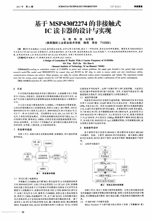
针对传统 的射频识别技术 的读卡器的设计 , 大多射 频卡的工作频
率 为 15 Hz功 耗 很 大 , 2k , 因此 要 求 应 答 器 的 线 圈 必 须 达 到 几 百 匝 , 由 此 产 生 的 较 大 绕 线 界 面及 需 要 附 加 的 电 容 器 很 难 封 装 在 小 型 塑 料 卡
【 摘 要】 针对非接触式 1 . M 读写器在功耗高、 35 6 体积大等方面问题 , 出了一种低功耗 、 提 高安全性的研究模型。模 型采 用 MS 40 2 7 P3F24 为 主 控 芯 片和 MFRC5 2为 射 频 芯 片 . 保 证 通 信 稳 定 、 干 扰 力 强 、 信 距 离能 达 到 1c 的 前 提 下 , 以 使 系统 有 效 降低 功耗 和体 积 。 实 2 在 抗 通 0m 可 经
M_ h HAN Ja M A Ha _i A Ya i o】
(h n x l i t f c n lg , ’nS a n i7 0 0 ) S a n i st eo Teh ooy Xia h a x ,13 2 h tu
【 src ] codn ocnat s rae f1.6 n pw ra d vlm rbe s h ae usfr ada l pw rhg eui AbtatA crig t otcl s edro 35 MHzi o e n ou e po lm ,te pp rp t ow r o o e ih scry e w— t
21 0 1年
第2 1期
S INC CE E&T C N L YIF R TO E H O OG O MA息
基于MSP430控制的射频识别读写器设计_英文_

第28卷 第2期吉首大学学报(自然科学版)Vol.28 No.2 2007年3月J ournal of J ishou University (Natural Science Edi ti on)Mar.2007 Article ID :1007-2985(2007)02-0059-04Design of RFID Reader Based on MCUMS P 430GE NG Shu qin,HOU Li gang,GUO Yue,W ANG Xiu ling,W U Wu chen(VLSI and System Lab,Beijing Universi ty of Technology,Beijing 100022,China)Abstract :Saving power is an important problem in portable device.This paper presents a SOC (System on a Chip)sys tem for radio frequency identification (RFID)reader to simplify the complex traditional circuits.It puts the peripheral circuits into SOCand uses software to e xec ute the decoding,checking,identifying and real time calculating and display ing of digital signals.The proposed system has advantages such as simple structure,low cost,and low power consump tion.Key words :RFID;reader;lo w power consumptionCLC number :TN47 Document code :B1 IntroductionRFID is one of automatic technology to identify and collect objec t data quickly through RF digital signals.RFID increases productivity and convenience.RFID is used for hundreds,if not thousands,of applications such as preventing theft of automobiles and merchandise,gaining entrance to buildings,automating parking [1],and so on.The thoughts of RFID occurred on the heels of the development of radar.An early,if not the first,work exploring RFID is the landmark paper by Harry Stockman, Communication by Means of Reflected Power published in 1948[2].RFID has advantages over bar code [3]:RFID does not require line of sight access to read the tag;the read range ofRFID is larger than that of a bar c ode reader;readers can simultaneously communicate with multiple RFID tags;be cause of this capability,a RFID reader can capture the contents of an entire shipment as it is loaded into a warehouse or shipping c ontainer;a reader collects detail information in one pass,without having to scan each product;tags can store more data than bar c odes.F ig .1 Block D iagram of a General Passive RFID System In general,RFID system comprises a reader (or interrogator),its associa ted antenna and the transponder (ortag)that carries data (see fig.1).Depending on theirsource of electrical power,there are active and passive twogeneral categories.Active RFI D ta gs contain an on boardbattery.Passive ta gs obtain po wer from the signal of reader.This paper deals with the passive ta g reader of 125kHz.The reader is usually controlled by micro controller of MC S51or arm.The former has high voltage,and much pow Received date :2007-01-20Foundation item :T he National Reform Commi ttee of Development Next Internet Demonstrative Subproject (CNGI-04-10-1D)Biography :GENG Shu qin(1970-),female,was born in Yuncheng City,Shaanxi Province,a doctor s tudent in Beijing University of Technology;the major research areas are the field of system integration,sensor and RFID.er c onsumption,with many peripheral circuits in the control system of RFID reader.It is not convenient to adjust the system and the area of PCB is big.The latter has high price,and the c ontrol system is complex.This paper presents a RFID reader system based on MSP430,which puts much peripheral circuits into a chip.It uses software to e xecute the decoding,checking,identifying and real time calculating and displaying of digital signals.The proposed syste m has ad vantages such as simple structure,low cost,and low power consumption.2 Functions of System2.1The Passive Tag ReaderThe reader is composed of RF. Module and micro controller (see fig.1).The reader transmits a low power radio signal through its antenna of RF. Module.When a tag c omes within the reader !s range,it receives an electromagnetic signal from the reader through the tag !s antenna.The tag then stores the energy from the signal,a process called inductive coupling [3].When the tag has built up enough charge,it can po wer a back end integrated circuit (chip)of the tag,which transmits a modulated signal to the reader.That return signal contains the information stored in the tag.Once the RF. Module received the data it can be sent to a micro c ontroller (or computer)for processing and management.At the same time,the processed data will be sent to LCD for display.2.2Communication Between Reader and TagBiot Savart la ws establish the relationship between the current I 1flowing in an electrical circuit having length l and the intensity of the magnetic induction B as function of the distance x be tween the measurement P point (of unit vector z ,shown in fig.2)and the element dl producing the field according to the formula [4]:d B = 0(I 1∀d l )#e z 4 x 2.Fig .2 Magnetic Field Strength F ig .3 Electric Equivalent Circuits for Magnetic(the Axis of the Coil )Coupling of Reader and Tag z is the axis of the coil.The total intensity of the magnetic induction of reader antenna is:B z (d ,r )= 0N 1I 1r 22(r 2+d 2)3/2.The electric equivalent circuit for Magnetic Coupling of Reader and tag is depicted in fig.3.As the previous sec tion has shown,this system works on the principle of Magnetic Coupling.The reader antenna resonant circuit is con structed by a capacitor C 1with an inductance L 1and the resistance R 1.The circuit of tag antenna is simplified as L 2,R 2,with the capacitance C 2,and the data load R L[4].Where para meter I shows the current of antenna;U 1is the source of ac signal voltage;U 2is the load voltage.The subscript 1indicates the side of reader;the subscript 2denotes the side of tag.The voltage of reader antenna is U 1= L 1I 1= !1.When tag enters the field of reader,such as P point,the flux that goes through tag antenna is !2=B Z S 2N 2.Acc ording to Faraday !s Law,if !2(t )=B Z S 2N 2=!2sin( t ),then u 20(t )=-d !2(t )/d t = !2cos( t ).Value of the coupling coefficient is M =k L 1L 2.The relation of signal volt 60吉首大学学报(自然科学版)第28卷age between reader and tag antenna is:U 20/U 1=k L 2/L 1.3 S ystem Architecture3.1Reader SystemFig .4 Reader System Frame of MSP 430F 435Reader syste m frame is consisted of RF. Module,LCD,keys,MC UMSP430and power.Reader system fra meof MSP430is shown as in fig. 4.This syste m uses lowpower consumption MC UMSP430that is a system on chipas the controller.The voltage is at 1.8~3.6V.3V ischosen by this system.The MSP430ultra lo w po wer architecture e xtends battery life.Current of RAM retention is0.1 A;a real time clock mode current is 0.8 A;currentof active state is 250 A 1MlPS.The clock system is de signed specifically for battery po wered applications.A lo w frequency auxiliary clock (ACLK)is driven directly from a common 32kHz watch crystal.The ACLK can be used for a background real time clock self wake up function.This low frequency auxiliary clock makes stand by mode ultra low power.An integrated high speed digitally controlled oscil lator (DCO)can source the master cloc k (MCLK)used by the CP U and high speed peripherals.By design,the DC O is active and stable in less than 6 s.This high speed master clock achieves high performance signal processing.MSP430 based solutions effectively use the high performance 16 bit RISC C PU in very short bursts.MSP430has LCD controller,which can directly drive LCD displays.It simplifies the complex circuits of traditional electrical LCD display system and solves the additional error problems.It puts the peripheral circuits into SOC.This can reduce the area and power consumption of PCB and minify the portable RFID system.Fig.3shows RF. Module c ommunicating with MCUMSP430.It can be seen that LC D module is linked with MSP430by I O in fig. 3.LCD gets data from I O of MC UMSP430and then displays them.W hen there is ta g in the reader radio field,RF. Module will receive signals.At the same time,the interrupt will wake up CP U in less than 6 s.Then CPU processes da ta and LCD displays them.When CPU has operated the interrupt,it will be set in the ultra low power stand by mode by the software.If there is not tag for a long time,LCD display is set to low po wer state.There are 20keys in this system,which are linked with CPU.RF. Module and Ke ys are connected with the interrupt pins.If there is no interrupt signals,system are in lo w power state.The soft frame is shownin fig.5and fig.6.Fig .5 Reader System Software Frame Fig .6 Identification Subprogram of Interruption3.2Communication Between RF . Module and MC UThe communication between RF. Module and MC U is as in fig.7:There is one byte as the start data and one 61第2期 耿淑琴,等:基于MSP430控制的射频识别读写器设计byte as the end data.The middle part is the ciphered data and longitudinal redundancy check (LRC)[5]data.RF.Module data and LRC data are sent together to the MC U.When their XOR result is zero,the data is right.Then data are sent to LC D for display,decoding and processing them.For example,one ta g I D number is 51E2066CED.Their ci phered c odes are 35H,31H,45H,32H,30H,36H,36H,43H,45H,and 44H.Longitudinal redundancy checksum is (51H)XOR (E2H)XOR (06H)XOR (6C H)XOR (EDH),and the checksum equals 34H.Together with the start bit 01,ciphered data,checksum and stop bit 02,the total number is 01353145323036364345443402.If MCU MSP430gets the data,it must take out the ciphered data with the checksum data,and execute the longitudinal redun dancy check.If the checksum of MC U is zero,it will decode the ciphered da ta.Identifying,real time calculating and displaying of digital signals must be carried out.If the checksum of MCU is not zero,this means that there are some er rors in the data.Then MCUMSP430will ask the RF. Module to send the data again.start bit Ciphered data Checksum stop bitFig .7 Data F orm Between RF . M odule and MC UFig .8 Data TimingIf MC U wants to get data correctly,it must applywith the data timing as fig.8.Clock frequency must beset seriously,and the time of instruc tors must be calculated correctly.Or else,experiment data may be wrong.Itwill take a lot of time to adjust and do experiments.4 ExperimentsTable 1sho ws power consumption of CP U and system at different state.W hen CPU is at stand by state,current is the ac tive state !s 39.2%.Power c onsumption of the stand by state can be reduced to 61%of the active state.Table 1 CPU Power Consumption of 125kHz RFID SystemCPU StateCPU I m A Power Consumption mW Active0.0280.61600Stand by LP30.0110.02420Sleeping 0.0100.000225 SummaryThis paper presents a RFID reader system for 125kHz to simplify the complex circuits of traditional system and to solve the additional error problems.It puts the peripheral circuits into SOC and uses software to execute the dec oding,checking,identifying and real time calculating and displaying of digital signals.The proposed system has advantages such as simple structure,low cost,and low power consumption.This system is successfully used in 125kHz RFID.References :[1] LANDT J.POTENTIALS.IEEE.History of RFID [J].Potentials,IEEE,2005,24(4):8-11.[2] HARRY municati on by Means of Reflected Power [J].Proceeding of the I.R.E,1948,36:1196-1204.[3] RAO K V S.An Overview of Backscattered Radio Frequency Iden tification System (RFID)[J].IEEE Microwave Conference,AsiaPaci fic,1999,3:746-749.[4] DOMINIQUE PARET.Translated by Roderick Riesco,RFID and Con tactless Smart Card Applications [M].England:John Wiley &Sons Ltd.,2005.[5] CORR P.A Statistical Evaluation of Error Detection Cyclic Codes for Data Transmissi on [J].Transactions on Communications Systems,1964,49:211-216.(下转第74页)Teleportation of Two Partite Arbitrary States Via GenuineFour Partite Entangled StatesKONG Yong hong,W ANG Xin wen(Department of Electronic Engineering and Physics,Hunan Uni versity of Science and Engineering,Yon gzhou425100,Hunan China)Abstract:A scheme for teleportation of two partite arbitrary states via genuine four partite entangled states is proposed. In the sche me,16orthogonal and complete bases are constructed.All the bases are genuine four partite entangled states,none of which is reducible.The scheme reveals some particular properties of the rela ted four partite entangled state,and indicates that in some sense the amount of entanglement of two Bell states can be abstracted from any one of the four partite states.Key words:four partite entangled states;two partite arbitrary states;orthogonal and complete bases;teleportation(责任编辑 陈炳权) (上接第62页)基于MSP430控制的射频识别读写器设计耿淑琴,侯立刚,郭 跃,王秀玲,吴武臣(北京工业大学集成电路与系统实验室,北京 100022)摘 要:设计了一种基于单片机处理器的射频识别(RFID)便携式读写器的系统.采用当前先进的片上系统(System on Chip,SOC),将外围电路尽可能地放置于SOC芯片内,利用软件实现了对射频标签信号的数字实时采集和控制功能,从而简化了传统的微控制器控制的RFID读写器所需的庞大硬件电路及其引入的额外误差,具有重要的实用价值,并且功耗和成本很低.关键词:射频识别;读写器;低功耗中图分类号:TN47文献标识码:B(责任编辑 陈炳权)。
基于MSP430的手持式RFID读写器的设计

2010年5月内蒙古大学学报(自然科学版)May2010第41卷第3期Journal of Inner Mongolia University Vol.41No.3 文章编号:1000-1638(2010)0320346205基于MSP430的手持式RFID读写器的设计3潘盛辉,郭毅锋,潘绍明,黄丽敏(广西工学院电子信息与控制工程系,广西柳州545006)摘要:根据识别目标位置不固定不宜采用固定式系统的应用要求,设计了一种基于MSP430单片机的手持式RFID读写器.在介绍RFID读写器组成结构的基础上,重点介绍MSP430F149单片机采用SPI接口方式与RF收发芯片FM1702SL的硬件接口及相应软件的设计方法.应用表明,该手持式RFID读写器的设计达到相应的技术指标要求,具有良好的市场应用前景.关键词:MSP430单片机;手持式RFID读写器;FM1702SL;SPI接口;低功耗中图分类号:TP306 文献标志码:A引 言 射频识别RFID(Radio Frequency Identification)技术是利用无线射频方式进行非接触式双向通信,以达到识别目标和交换数据的目的,实现对各种对象在不同状态下的自动识别和管理的一种技术.RFID系统一般包含射频标签(或称射频卡)、读写器和应用管理系统组成.其中,射频标签具有扫描快,体积小、易封装,抗污染能力和耐久性,可重复使用,穿透性和无屏阅读,数据的记忆容量大,安全等特点.目前广泛应用于在身份识别和门禁管理、防伪、商业供应链、公共交通管理、物流管理、生产线的自动化及过程控制、动物的跟踪及管理、容器识别等领域〔1〕.在门禁管理、生产线自动控制、封闭库房等领域中识别对象的位置相对固定或者所经路径相对确定,所使用的RFID系统一般可采用固定式读写设备,便于与计算机系统相连,并由计算机系统对识别对象进行管理.但在许多场合,由于使用环境特殊、安装布线不便等原因,读写设备难与计算机系统相连接使用,特别是被识别的目标是位置不固定,且路径不确定,需要在一定范围内移动读写设备,例如身份识别应用中RFID电子标签式的身份证随持证人而流动,车辆识别管理应用中RFID电子标签随车辆运行或停放而流动,防伪检查应用中商品因销售渠道而流动、动物跟踪应用中因动物的迁移而流动等,在这些应用场合中射频标签随被识别目标的流动而不断改变位置,固定式读写设备很难适应应用要求.为适应不宜安装固定式RFID系统的应用环境的需要,RFID读写器一般设计成手持式读写设备.同时,为满足不同的具体应用领域需要,本设计中的手持式RFID读写器是可进行二次开发的通用读写设备,接口功能齐全,便于根据具体应用的需要可进行相应的二次开发,具有比较大的灵活性.本文着重介绍手持式RFID读写器中MSP430单片机与射频收发模块接口的硬件设计方法,以及系统软件中主程序、RF收发模块的初始化程序、射频卡的读/写操作程序的设计方法.1 系统工作原理及性能指标手持式RFID读写器通常由操作人员手持设备在某一区域内完成对射频标签相关信息的采集及3收稿日期:2008211212;修回日期:2009210222基金项目:广西自然科学基金资助项目(桂科自0832066);广西工学院科学基金资助项目(院科04010)作者简介:潘盛辉(1971-),男(侗族),广西柳州市人,副教授.显示,并将相应数据存储于读写器的存储器中,待与计算机连接后通过串行通信接口或U SB 接口传送到本地计算机,也可通过网络接口传送到远程的网络计算机,以便计算机系统进行相应的数据处理及应用.手持式RFID 读写器不涉及具体应用领域,只是针对通用的RFID 系统功能进行RFID 读写器的设计,提供为二次开发所需的读写RFID 标签的基本功能及相应接口模块.主要性能指标如下:通信协议:支持ISO14443typeA 协议工作频率:13.56M Hz读写距离:>10mm扩展集成存储器:2M Bytes 存储量通信接口与速率:RS 2232接口,57600bp s ;U SB 接口,2M ;以太网络接口:10M/100M支持射频标签类型:M IFA RE 卡防冲突功能:有,可用于寻卡操作天线:内置式读写天线显示:OL ED 显示器,4行中文电源电压:AC 适配器、U SB 供电、充电电池供电,电压+3.3V 及+5V工作温度:-10~+65℃.2 系统硬件设计2.1 系统硬件总体设计为满足不同领域的应用需求及可针对具体应用进行二次开发设计需要实现各种功能的要求,手持式RFID 读写器主要由主控制模块、RF 收发模块、显示模块、实时时钟模块、扩展存储模块、U SB 接口模块、串行通信模块、以太网络接口模块、键盘模块及电源系统等组成,其硬件组成结构图如图1所示.图1 RFID 读写器组成结构图Fig.1 Block diagram of RFID reader2.2 主控模块 主控模块负责执行读写器命令、对发送信号进行编码和对接收信号进行解码,完成射频标签的正确识别.MCU 选用具有超低功耗特性且功能强大的MSP430F149单片机,具有易于控制的5种低功耗工作模式,工作电压为1.8~3.6V 〔223〕.为优化系统的低功耗特性,在手持式RFID 读写器设计中在相应程序中可根据不同的工作状态,MSP430可由软件选择不同的时钟源和不同频率作为系统程序运行工作时基、FL ASH 读写操作时基、实时时钟和低功耗的的备用工作时钟频率〔425〕.MSP430F149提供了6个通用并行端口P1~P6,其中P1、P2具有中断功能、P3、P5支持同步通信(SPI )模式的接口功能,一个看门狗定时器WD T 、两个16位定时器模块TA 及TB 、两个串行通信模块U SA R T0及U SA R T1等,可以满足外围模块的接口需要.743第3期潘盛辉等 基于MSP430的手持式RFID 读写器的设计2.3 RF 收发模块及其接口射频收发模块由天线、射频读写芯片及其相应外围电路组成,以实现控制器与射频卡的通信.本设计中射频读写芯片采用复旦微电子公司的基于ISO14443标准,支持13.56M Hz 频率下的typeA 非接触通信协议,支持MIFA RE 标准加密算法的专用芯片FM1702SL.该芯片内部高度集成了模拟调制解调电路,只需最少量的外围电路,数字电路具有T TL/CMOS 两种电压工作模式.数字、模拟和发射模块都有独立的电源支持宽电压(3V 25V ),功耗低,具有硬件电源关闭、软件电源关闭及待机等三种省电工作模式,包含512字节的EEPROM 、64字节的FIFO ,支持SPI 接口模式,具有一个中断处理器.特别适用于ISO14443标准下需进行数据读写系统的读写器的应用.图2 MSP430F149与FM1702SL 接口原理图Fig.2 Interface of MSP430F149and FM1702SL MSP430F149单片机与FM1702SL 芯片的接口原理图如图2所示.MSP430F149的P3.0~P3.3用作SPI 接口与FM1702SL 进行连接,负责完成RF 收发通信的数据读写操作,其中FM1702SL 作为SPI 从设备必须满足相应的SPI 时序要求.相应的射频信号匹配电路包括EMC 低通滤波电路、接收电路、天线匹配电路及天线等,其中低通滤波电路用于晶振输出的高频谐波的滤波以满足国际EMC 规则的规定要求.为了优化系统性能,天线匹配电路设计时要考虑天线的电阻、导体的厚度、线与线之间的距离、保护层材料的使用等因素.2.4 电源系统为便于针对具体应用场合与应用系统计算机的数据通信的需要,还提供了U SB 接口、串行通信接口、以太网络接口等通信接口,二次开发时可根据需要适当选择是否需要保留.同时,为扩大手持式RFID 读写器的可工作范围以适应不同场合的应用,手持式RFID 读写器电源系统采用了U SB 电源、AC 电源以及电池供电相结合的模式,以便为RFID 系统进行供电、充电.2.5 其他模块扩展存储模块是用于在某些数据存储量大的应用中因单片机的存储器容量有限,而手持式读写器单独使用时保存读取射频标签的数据,以便于连接到计算机上后上传数据,同时也可以保存用于显示的用户字库,选用A T45DB161B 串行FL ASH 存储器.键盘与显示模块用于输入或显示相关的射频识别系统的相关信息,实现用户操作所需的人机界面,显示模块及驱动芯片选用P13501显示模块(含内置驱动芯片SSD1303),通信模块用于与计算机进行通信,其中U SB 接口选用IPS1582,串行通信接口选用MAX3232、网络接口模块选用ENC28J 60.实时钟模块用于记录特定事件记录和操作的日期时间,为应用系统提供准确的日期时间.3 系统软件设计手持式RFID 读写器的软件包括系统各模块的初始化程序、射频卡读/写程序、数据存储/处理程序、各种通信程序、键盘/显示程序、实时时钟程序等,相应的程序及数据可分别安排保存于单片机片内FL ASH 及扩展的FLASH 中,便于二次开发或应用中进行软件更新.下面重点介绍主程序及RF843内蒙古大学学报(自然科学版)2010年接口初始化程序的设计方法及射频卡读/写操作流程.图3 RFID 读写器的主程序流程图Fig.3 Main flow chart of RFIDreader 图4 FM1702SL 初始化流程图Fig.4 Initialization flow chart of FM1702SL图5 读射频卡流程图Fig.5 Flow chart of RF cardreading 图6 写射频卡流程图Fig.6 Flow chart of RF card writing3.1 主程序及RF 接口初始化程序设计主程序主要完成MSP430F149及其相应外围模块接口所需的初始化工作,并等待用户通过键盘操作完成相应的软件更新、射频卡读/写,信息显示、数据通信等操作.读写器在完成初始化后,由用户设置工作模式,其中射频模式下读写器通过发射天线发送一定频率的射频信号,当附着标签的目标对象进入发射天线工作区域时会产生感应电流,射频标签凭借感应电流所获得的能量发送出存储在芯片中的信息,或主动发送某一频率的信号;射频标签将自身编码等信息通过内置发送天线发送出去;系统接收天线接收到从射频标签发送来的载波信号,经天线调节器送到读写器,读写器对接收的信号进行解调和解码后,进行相关处理.主程序流程图如图3所示. FM1702SL 支持可编程启动配置,其启动过程是在上电复位或复位管脚RSTPD 加高电平使其943第3期潘盛辉等 基于MSP430的手持式RFID 读写器的设计053内蒙古大学学报(自然科学版)2010年进入硬件掉电模式阶段,随后自动进入复位阶段,部分相应寄存器由硬件预置,复位后进行初始化,由软件完成相应的寄存器设置.其初始化流程图如图4所示.3.2 射频卡读写程序设计FM1702SL支持ISO14443typeA通信协议,其C语言开发的底层函数库中提供了基本命令函数,便于实现射频卡的侦测(REQU EST)、防冲突检测(AN TICOLL SION)、选卡(SEL ECT)、密码认证(AU T H EN TICA TION)、读卡(READ)、写卡(WRITE)及停卡(HAL T)等操作.射频卡信息的读取、写入操作流程图分别如图5、图6所示.在相应的读写操作后还要对所选射频卡发送停卡命令,使其退出工作.4 结束语手持式RFID读写器采用了具有低功耗的MSP430F149单片机及FM1702SL射频收发芯片为核心进行低功耗设计,实现了支持ISO14443标准的射频卡读写、人机界面操作等基本功能,并提供了U SB、RS232、网络通信接口.软件开发采用C语言,提高软件开发的工作效率及程序的可靠性、可读性和可移植性.经应用证明,本系统的设计达到相应的性能指标,并具有功耗低、便于二次开发成不同的射频识别应用系统等特点,具有良好的市场应用前景.参考文献:[1] 郎为民.射频识别(RFID)技术原理与应用[M].北京:机械工业出版社,2006.[2] 胡大可.MSP430系列FL ASH型超低功耗单片机[M].北京:北京航空航天大学出版社,2001.[3] 沈健华,杨艳琴,翟骁曙.MSP430系列16位超低功耗单片机实践与系统设计[M].北京:清华大学出版社,2005.[4] 张挺,熊璋,王剑昆,等.一个面向低功耗设计的RFID系统研究与实现[J].小型微型计算机系统,2006(11):209022093.[5] 李和平,黎福海.基于MF RC500的Mifare射频卡读写器设计[J].电测与仪表,2007(9):61264.Design of Handheld RFID Reader Based on MSP430PAN Sheng2hui,GUO Y i2feng,PAN Shao2ming,HUAN G Li2min(De p artment of Elect ronic I nf orm ation and Cont rol Engi neeri n g,Guang x i Universit y of Technolog y,L i uz hou545006,Chi na) Abstract:To meet t he requirement of different appliactions t hat t he fixed RFID reader is not suitable to be installed for identified object s in unfixed position,a handheld RFID reader is designed based on MSP430F149MCU and FM1702SL RF t ransceiver.The software and t he hardware inter2 face using SPI mode for MSP430F149to cont rol FM1702SL are p resented in detail.The application indicates t hat it s technical parameters meet t he design requirement s,and it will have t he good mar2 ket application p rospect. K ey w ords:MSP430MCU;handheld RFID reader;FM1702SL;SPI mode;low power consump2 tion。
基于MSP430控制的射频识别读写器设计

基于MSP430控制的射频识别读写器设计耿淑琴;侯立刚;郭跃;王秀玲;吴武臣【期刊名称】《吉首大学学报(自然科学版)》【年(卷),期】2007(28)2【摘要】Saving power is an important problem in portable device.This paper presents a SOC (System on a Chip) system for radio frequency identification (RFID) reader to simplify the complex traditional circuits.It puts the peripheral circuits into SOCand uses software to execute the decoding,checking,identifying and real-time calculating and displaying of digital signals.The proposed system has advantages such as simple structure,low cost,and low power consumption.%设计了一种基于单片机处理器的射频识别(RFID)便携式读写器的系统.采用当前先进的片上系统(System on Chip,SOC),将外围电路尽可能地放置于SOC芯片内,利用软件实现了对射频标签信号的数字实时采集和控制功能,从而简化了传统的微控制器控制的RFID读写器所需的庞大硬件电路及其引入的额外误差,具有重要的实用价值,并且功耗和成本很低.【总页数】5页(P59-62,74)【作者】耿淑琴;侯立刚;郭跃;王秀玲;吴武臣【作者单位】北京工业大学集成电路与系统实验室,北京,100022;北京工业大学集成电路与系统实验室,北京,100022;北京工业大学集成电路与系统实验室,北京,100022;北京工业大学集成电路与系统实验室,北京,100022;北京工业大学集成电路与系统实验室,北京,100022【正文语种】中文【中图分类】TN47【相关文献】1.基于FM1715的射频识别读写器的设计与实现 [J], 张亚君;陈龙;叶勇威2.一种用于射频识别读写器的微波发射功率增益控制器的设计 [J], 张建明;赖声礼3.基于多协议的射频识别读写器设计 [J], 王赜坤4.基于USB-Host的射频识别读写器的设计 [J], 高丙坤;宋传军;许明子5.基于微波射频识别的物联网前端读写器设计研究 [J], 韩俊因版权原因,仅展示原文概要,查看原文内容请购买。
基于MSP430的低功耗无线射频识别装置

基于MSP430的低功耗无线射频识别装置
张宝瑛;王子超;李京忠;李晓燕
【期刊名称】《现代仪器与医疗》
【年(卷),期】2010(016)005
【摘要】本装置是由阅读器、应答器和耦合线圈组成的低功耗被动式无线识别系统.其中应答器为无源装置,通过线圈的互感效应提供能量,来实现指令发射、信息存储、发射以及为超低功耗的MSP430单片机供能.通过控制与非门来对信号进行负载调制,实现阅读器对应答器的识别,阅读器与应答器之间的数据传输以及数据存储功能.电路简单、功耗低、效率高是本装置的亮点.
【总页数】3页(P78-79,82)
【作者】张宝瑛;王子超;李京忠;李晓燕
【作者单位】北京中医药大学信息中心,北京100029;北京交通大学电子信息工程学院,北京100044;北京中医药大学信息中心,北京100029;北京中医药大学信息中心,北京100029
【正文语种】中文
【中图分类】TH83
【相关文献】
1.基于MSP430单片机的低功耗无线温度表的设计 [J], 于文刚;王海国;李小影;马操
2.基于MSP430与HC06的低功耗无线温湿度检测系统 [J], 章腾辉
3.基于MSP430单片机的低功耗射频识别系统 [J], 易金桥;谭建军;廖红华;黄勇
4.温室超低功耗无线传感器智控系统设计——基于MSP430和ZigBee [J], 魏纯;刘红艳
5.基于MSP430的便携式低功耗无线读写器的设计 [J], 胡双喜
因版权原因,仅展示原文概要,查看原文内容请购买。
基于MSP430的射频卡读写系统设计与实现

2 .T e c h n o l o g y C e n t r e R &D D e p a r t me n t , J i a n g x i S a n c h u a n Wa t e r Me t e r C o . , L t d . ,Y i n g t a n 3 3 5 0 0 0, C h i n a )
邹方卫 , 宋高 俊 , 宋财华2
( 1 . 南 昌航 空大学信 息工程 学院, 江西 南昌 3 3 0 0 6 3 ; 2 . 江西三川水表股份 有限公 司技术 中心研发部 , 江西 鹰潭 3 3 5 0 0 0 ) 摘要 : 基 于 MS P 4 3 0单 片机 开发 一种 T 5 5 5 7射频卡读 写 系统。为 了实现仪表应 用的低 成本、 低功耗和 高可靠性要 求 , 利用
2 0 1 3年第 5期
文章编号 : 1 0 0 6 - 2 4 7 5 ( 2 0 1 3 ) 0 5 - 0 2 2 7 - 0 4
计 算 机 与 现 代 化 J I S U A N J I Y U X I A N D A I H U A
总第 2 1 3期
基 于 MS P 4 3 0的射 频 卡读 写 系 统设 计 与 实 现
g e n e r a t e 1 2 5 k Hz s i g n a l ,wh i c h i s a mp l i i f e d b y p o w e r nd a mo d u l a t i o n t o p r o v i d e p o we r a n d d a t a f o r RF c a r d ;W h i l e t a k i n g a d v a n -
Ab s t r a c t :A ' 1 5 5 5 7 RF c a r d s y s t e m b a s e d o n mi e me o n t r o l l e r MS P 4 3 0 i s d e v e l o p e d .I n o r d e r t o a c h i e v e l o w c o s t , l o w p o we r c o n -
基于MSP430的RFID读写器的设计

基于MSP430的RFID读写器的设计王鲲鹏;王啸林【期刊名称】《现代计算机(专业版)》【年(卷),期】2012(000)014【摘要】设计一种基于MSP430单片机的多协议RFID读写器。
分析RFID概念、应用现状及系统构成,介绍两款主要芯片的功能特点,给出系统硬件组成结构.提出系统的软件组成模块及软件流程图。
系统顺利通过测试,其设计达到相应的技术指标要求,具有良好的市场应用前景。
%Designs a multi-protocols RFID reader system based on MSP430, and analyses the conception, application status and system structure of RFID. Introduces the functions and characteristics of two main chips, provides the structure of the hardware, and puts forward the software blocks and software flow diagram. System tests indicate that the system design can meet the requirement of basic technical design, and it will be found wide application in the future.【总页数】3页(P71-73)【作者】王鲲鹏;王啸林【作者单位】常州市软件技术研究与应用重点实验室,常州213002/常州工学院计算机信息工程学院,常州213002;武汉市燃气热力规划设计院,武汉430015【正文语种】中文【中图分类】TP368.1【相关文献】1.基于MSP430的手持式RFID读写器LCD接口设计 [J], 潘盛辉;郭毅锋;黄丽敏2.基于MSP430F149的手持式RFID读写器低功耗设计 [J], 潘盛辉;郭毅锋;黄丽敏;潘绍明3.MSP430F449在基于RFID技术的射频标签读写器中的应用 [J], 许博;高树东;赵起超4.基于MSP430的便携式低功耗无线读写器的设计 [J], 胡双喜5.基于MSP430的手持式RFID读写器的设计 [J], 潘盛辉;郭毅锋;潘绍明;黄丽敏因版权原因,仅展示原文概要,查看原文内容请购买。
基于MSP430的手持式RFID读写器LCD接口设计

第19卷 第2期 广西工学院学报 Vol119 No12 2008年6月 JOURNAL OF GUAN GXI UN IV ERSIT Y OF TECHNOLO GY J un12008 文章编号 100426410(2008)022*******基于MSP430的手持式RFID读写器LCD接口设计潘盛辉,郭毅锋,黄丽敏(广西工学院电子信息与控制工程系,广西柳州 545006)摘 要:根据MSP430F149单片机和SED1335液晶控制器的性能特点,设计了基于MSP430F149单片机的手持式RFID读写器的液晶显示接口。
并论述了LCD接口的硬件设计方法和软件设计方法,给出了相应的硬件接口电路和按照显示控制时序设计的控制程序流程图。
关 键 词:MSP430单片机;RFID读写器;LCD接口中图分类号:TP3O6 文献标识码:A0 引言RFID技术目前广泛应用于身份识别、防伪应用、供应链管理、公共交通管理、物流管理、生产线自动化与过程控制、容器识别等领域[1]。
根据不同的应用要求,RFID系统的具体功能有所差别。
而RFID卡(电子标签)的信息显示是读写器的主要功能之一[2],本课题研究的是通用的手提式RFID读写器,因而系统显示器应选用具有功耗低、体积小、重量轻、超薄等优点的液晶显示器。
本文论述了RFID读写器中MSP430单片机与LCD模块接口的硬件设计的方法,以及LCD显示相关信息的软件设计方法。
1 MSP430F149单片机性能特点MSP430F149是TI公司推出的16位系列单片机,能驱动液晶多达120段,超低功耗使其在用电池供电的便携式设备应用中表现出非常优良的特性,非常合适于手持式RFID读写器。
片内数控振荡器可以调整MSP430F149单片机的工作频率,以适应不同外设的需求,提高了系统的利用效率;大容量的片内存储器使得系统在不需要外加存储设备的情况下就能实现大规模数据的存储,使得能够设计出内容丰富、美观的手持式RFID读写器的LCD显示界面。
- 1、下载文档前请自行甄别文档内容的完整性,平台不提供额外的编辑、内容补充、找答案等附加服务。
- 2、"仅部分预览"的文档,不可在线预览部分如存在完整性等问题,可反馈申请退款(可完整预览的文档不适用该条件!)。
- 3、如文档侵犯您的权益,请联系客服反馈,我们会尽快为您处理(人工客服工作时间:9:00-18:30)。
第28卷 第2期 吉首大学学报(自然科学版)V ol.28 N o.2 2007年3月Journal of Jishou University (Natural Science Edition )M ar.2007 Article I D :1007-2985(2007)02-0059-04Design of RFID R eader B ased on MCUMSP 430ΞGE NG Shu 2qin ,H OU Li 2gang ,G UO Y ue ,W ANG X iu 2ling ,W U Wu 2chen(V LSI and System Lab ,Beijing University of T echnology ,Beijing 100022,China )Abstract :Saving power is an im portant problem in portable device.This paper presents a S OC (System on a Chip )sys 2tem for radio frequency identification (RFI D )reader to sim plify the com plex traditional circuits.It puts the peripheral circuits into S OCand uses s oftware to execute the decoding ,checking ,identifying and real 2time calculating and display 2ing of digital signals.The proposed system has advantages such as sim ple structure ,low cost ,and low power consum p 2tion.K ey w ords :RFI D ;reader ;low power consum ptionC LC number :T N47 Document code :B1 I ntroductionRFI D is one of automatic technology to identify and collect object data quickly through RF digital signals.RFI D increases productivity and convenience.RFI D is used for hundreds ,if not thousands ,of applications such as preventing theft of autom obiles and merchandise ,gaining entrance to buildings ,automating parking [1],and s o on.The thoughts ofRFI D occurred on the heels of the development of radar.An early ,if not the first ,w ork exploring RFI D is the landmark paper by Harry Stockman ,“C ommunication by Means of Reflected P ower ”published in 1948[2].RFI D has advantages over bar code [3]:RFI D does not require line 2of 2sight access to read the tag ;the read range of RFI D is larger than that of a bar code reader ;readers can simultaneously communicate with multiple RFI D tags ;be 2cause of this capability ,a RFI D reader can capture the contents of an entire shipment as it is loaded into a warehouse or shipping container ;a reader collects detail in formation in one pass ,without having to scan each product ;tags can store m ore data than bar codes.Fig .1 B lock Diagram of a G eneral P assive RFI D SystemIn general ,RFI D system com prises a reader (or in 2terrogator ),its ass ociated antenna and the transponder (ortag )that carries data (see fig.1).Depending on theirs ource of electrical power ,there are active and passive tw ogeneral categ ories.Active RFI D tags contain an on 2b oardbattery.Passive tags obtain power from the signal of reader.This paper deals with the passive 2tag reader of 125kH z.The reader is usually controlled by micro controller of MCS51or arm.The former has high v oltage ,and much pow 2ΞR eceived d ate :2007-01-20Found ation item :The National Reform C ommittee of Development Next Internet Dem onstrative Subproject (C NGI -04-10-1D )Biography :GE NG Shu 2qin (1970-),female ,was born in Y uncheng City ,Shaanxi Province ,a doctor student in Beijing University of T echnology ;the major research areas are the field of system integration ,sens or and RFI D.er consum ption ,with many peripheral circuits in the control system of RFI D reader.It is not convenient to adjust the system and the area of PC B is big.The latter has high price ,and the control system is com plex.This paper presents a RFI D reader system based on MSP430,which puts much peripheral circuits into a chip.It uses s oftware to execute the decoding ,checking ,identifying and real 2time calculating and displaying of digital signals.The proposed system has ad 2vantages such as sim ple structure ,low cost ,and low power consum ption.2 Functions of System2.1The P assive 2T ag R eaderThe reader is com posed of RF.2M odule and micro controller (see fig.1).The reader transmits a low 2power radio signal through its antenna of RF.2M odule.When a tag comes within the reader ’s range ,it receives an electromagnetic signal from the reader through the tag ’s antenna.The tag then stores the energy from the signal ,a process called induc 2tive coupling [3].When the tag has built up enough charge ,it can power a back 2end integrated circuit (chip )of the tag ,which transmits a m odulated signal to the reader.That return signal contains the in formation stored in the tag.Once the RF.2M odule received the data it can be sent to amicro controller (or com puter )for processing and management.At the same time ,the processed data will be sent to LC D for display.2.2Communication B etw een R eader and T agBiot 2Savart laws establish the relationship between the current I 1flowing in an electrical circuit having length l and the intensity of the magnetic induction B as function of the distance x between the measurement P point (of unitvector z ,shown in fig.2)and the element dl producing the field according to the formula [4]:d B =μ0(I 1・d l )×e z 4πx 2.Fig .2 Magnetic Field Strength Fig .3 E lectric Equivalent Circuits for Magnetic(the Axis of the Coil )Coupling of R eader and T agz is the axis of the coil.The total intensity of the magnetic induction of reader antenna is :B z (d ,r )=μ0N 1I 1r 22(r 2+d 2)3/2.The electric equivalent circuit for MagneticC oupling of Reader and tag is depicted in fig.3.As the previous sec 2tion has shown ,this system w orks on the principle of Magnetic C oupling.The reader antenna res onant circuit is con 2structed by a capacitor C 1with an inductance L 1and the resistance R 1.The circuit of tag antenna is sim plified as L 2,R 2,with the capacitance C 2,and the data load R L [4].Where parameter I shows the current of antenna ;U 1is the s ource of ac signal v oltage ;U 2is the load v oltage.The subscript 1indicates the side of reader ;the subscript 2denotes the side of tag.The v oltage of reader antenna is U 1=ωL 1I 1=ω<1.When tag enters the field of reader ,such as P point ,the flux that g oes through tag antenna is <2=B Z S 2N 2.According to Faraday ’s Law ,if <2(t )=B Z S 2N 2=<2sin (ωt ),then u 20(t )=-d <2(t )/d t =ω<2cos (ωt ).Value of the coupling coefficient is M =k L 1L 2.The relation of signal v olt 206吉首大学学报(自然科学版)第28卷age between reader and tag antenna is :U 20/U 1=k L 2/L 1.3 System Architecture3.1R eader SystemFig .4 R eader System Frame of MSP 430F 435Reader system frame is consisted of RF.2M odule ,LC D ,keys ,MC UMSP430and power.Reader system frameof MSP430is shown as in fig. 4.This system uses low 2power consum ption MC UMSP430that is a system on chipas the controller.The v oltage is at 1.8~3.6V.3V ischosen by this system.The MSP430ultra low 2power archi 2tecture extends battery life.Current of RAM retention is0.1μA ;a real 2time clock m ode current is 0.8μA ;currentof active state is 250μA Π1MlPS.The clock system is de 2signed specifically for battery 2powered applications.A low 2frequency auxiliary clock (AC LK )is driven directly from a comm on 32kH z watch crystal.The AC LK can be used for a background real 2time clock self wake 2up function.This low 2frequency auxiliary clock makes stand 2by m ode ultra low 2power.An integrated high 2speed digitally controlled oscil 2lator (DC O )can s ource the master clock (MC LK )used by the CPU and high 2speed peripherals.By design ,the DC O is active and stable in less than 6μs.This high 2speed master clock achieves high performance signal processing.MSP4302based s olutions effectively use the high 2performance 162bit RISC CPU in very short bursts.MSP430has LC D controller ,which can directly drive LC D displays.It sim plifies the com plex circuits of traditional electrical LC D display system and s olves the additional error problems.It puts the peripheral circuits into S OC.This can reduce the area and power consum ption of PC B and minify the portable RFI D system.Fig.3shows RF.2M odule communicating with MC UMSP430.It can be seen that LC D m odule is linked with MSP430by I ΠO in fig. 3.LC D gets data from I ΠO of MC UMSP430and then displays them.When there is tag in the reader radio field ,RF.2M odule will receive signals.At the same time ,the interrupt will wake up CPU in less than 6μs.Then CPU processes data and LC D displays them.When CPU has operated the interrupt ,it will be set in the ultra low 2power stand 2by m ode by the s oftware.I f there is not tag for a long time ,LC D display is set to low power state.There are 20keys in this system ,which are linked with CPU.RF.2M odule and K eys are connected with the interrupt pins.I f there is no interrupt signals ,system are in low 2powerstate.The s oft frame is shown in fig.5and fig. 6.Fig .5 R eader System Softw are Frame Fig .6 Identification Subprogram of I nterruption3.2Communication B etw een RF .2Module and MCUThe communication between RF.2M odule and MC U is as in fig.7:There is one byte as the start data and one16第2期 耿淑琴,等:基于MSP430控制的射频识别读写器设计byte as the end data.The middle part is the ciphered data and longitudinal redundancy check (LRC )[5]data.RF.2M odule data and LRC data are sent together to the MC U.When their X OR result is zero ,the data is right.Then data are sent to LC D for display ,decoding and processing them.F or exam ple ,one tag I D number is 51E2066CE D.Their ci 2phered codes are 35H ,31H ,45H ,32H ,30H ,36H ,36H ,43H ,45H ,and 44H.Longitudinal redundancy checksum is (51H )X OR (E2H )X OR (06H )X OR (6CH )X OR (E DH ),and the checksum equals 34H.T ogether with the start bit 01,ciphered data ,checksum and stop bit 02,the total number is 01353145323036364345443402.I f MC U MSP430gets the data ,it must take out the ciphered data with the checksum data ,and execute the longitudinal redun 2dancy check.I f the checksum of MC U is zero ,it will decode the ciphered data.Identifying ,real 2time calculating and displaying of digital signals must be carried out.I f the checksum of MC U is not zero ,this means that there are s ome er 2rors in the data.Then MC UMSP430will ask the RF.2M odule to send the data again.start bit Ciphered data Checksum stop bitFig .7 Data Form B etw een RF .2Module and MCUFig .8 Data Timing I f MC U wants to get data correctly ,it must applywith the data timing as fig.8.Clock frequency must beset seriously ,and the time of instructors must be calculat 2ed correctly.Or else ,experiment data may be wrong.Itwill take a lot of time to adjust and do experiments.4 ExperimentsT able 1shows power consum ption of CPU and system at different state.When CPU is at stand 2by state ,current is the active state ’s 39.2%.P ower consum ption of the stand 2by state can be reduced to 61%of the active state.T able 1 CPU Pow er Consumption of 125kH z RFI D SystemCPU S tateCPU I ΠmA P ower C onsumption ΠmW Active0.0280.61600S tand 2by LP30.0110.02420S leeping 0.0100.000225 SummaryThis paper presents a RFI D reader system for 125kH z to sim plify the com plex circuits of traditional system and to s olve the additional error problems.It puts the peripheral circuits into S OC and uses s oftware to execute the decoding ,checking ,identifying and real 2time calculating and displaying of digital signals.The proposed system has advantages such as sim ple structure ,low cost ,and low power consum ption.This system is success fully used in 125kH z RFI D.R eferences :[1] LANDT J.POTE NTI A LS.IEEE.History of RFI D [J ].P otentials ,IEEE ,2005,24(4):8-11.[2] H ARRY ST OCK M AN.C ommunication by Means of Reflected P ower [J ].Proceeding of the I.R.E ,1948,36:1196-1204.[3] RAO K V S.An Overview of Backscattered Radio Frequency Identification System (RFI D )[J ].IEEE Microwave C on ference ,AsiaPacific ,1999,3:746-749.[4] DOMI NI QUE PARET.T ranslated by R oderick Riesco ,RFI D and C ontactless Smart Card Applications [M].England :John Wiley &S ons Ltd.,2005.[5] C ORR P.A S tatistical Evaluation of Error Detection Cyclic C odes for Data T ransmission [J ].T ransactions on C ommunications Sys 2tems ,1964,49:211-216.(下转第74页)Teleportation of Tw o2P artite Arbitrary States Via G enuineFour2P artite E ntangled StatesK ONG Y ong2hong,W ANG X in2wen(Department of E lectronic Engineering and Physics,Hunan University of Science and Engineering,Y ongzhou425100,Hunan China)Abstract:A scheme for teleportation of tw o2partite arbitrary states via genuine four2partite entangled states is proposed. In the scheme,16orthog onal and com plete bases are constructed.All the bases are genuine four2partite entangled states,none of which is reducible.The scheme reveals s ome particular properties of the related four2partite entangled state,and indicates that in s ome sense the am ount of entanglement of tw o Bell states can be abstracted from any one of the four2partite states.K ey w ords:four2partite entangled states;tw o2partite arbitrary states;orthog onal and com plete bases;teleportation(责任编辑 陈炳权) (上接第62页)基于MSP430控制的射频识别读写器设计耿淑琴,侯立刚,郭 跃,王秀玲,吴武臣(北京工业大学集成电路与系统实验室,北京 100022)摘 要:设计了一种基于单片机处理器的射频识别(RFI D)便携式读写器的系统.采用当前先进的片上系统(System on Chip,S OC),将外围电路尽可能地放置于S OC芯片内,利用软件实现了对射频标签信号的数字实时采集和控制功能,从而简化了传统的微控制器控制的RFI D读写器所需的庞大硬件电路及其引入的额外误差,具有重要的实用价值,并且功耗和成本很低.关键词:射频识别;读写器;低功耗中图分类号:T N47文献标识码:B(责任编辑 陈炳权)。