散热器辐射分析研究
显卡散热器电磁辐射仿真和结构优化

计 算 机 辅 助 工 程
C o mp u t e r Ai d e d E n g i n e e r i n g
Vo 1 . 2 2 No . 5
0c t .2 0 1 3
文章编号 : 1 0 0 6—0 8 7 1 ( 2 0 1 3 ) 0 5 - O l 0 8 . 0 4
b u i l t b y ANS YS HFS S a n d t h e e f f e c t o f g r o u n di n g mo d e o n i t s r a di a t i o n i s a n a l y z e d; t h e p a r a s i t i c p a r a me t e r s b e t we e n h e a t s i n k a n d PCB a r e c a l c u l a t e d a n d t he he a t s i n k s ha p e i s o p t i mi z e d t o c h a n g e t h e r a d i a t i o n p a t t e r n, wh i c h r e d u c e s t h e e l e c t r o ma g n e t i c r a d i a t i o n e ic f i e n t l y . Th e t e s t r e s u l t s i n s hi e l d
E l e c t r o m a g n e t i c I n t e f r e r e n c e ( E MI )e a s i l y e x c e e d s t h e s t a n d a r d , t h e h e a t s i n k m o d e l o f a g r a p h i c s c a r d i s
低温热管墙壁辐射散热器及其应用探讨
1 前言
管上 半 部 的冷 源 中去 。但 是 , 力 热管 对其 倾斜 角 度有 一 定 重
限制 , 一般 要 求 热 管轴 向与 水平 方 向 的倾角 不小 于 1 5度 。
随 着 国民经 济 的发 展 和人 民生 活水 平 的提 高 , 业及 民 工
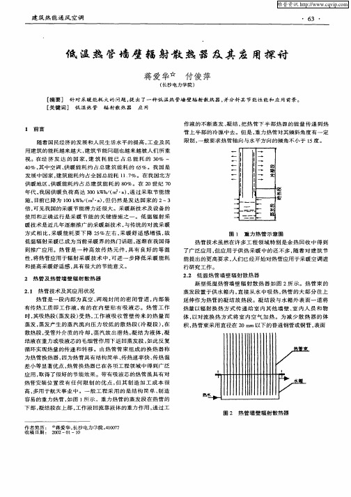
新 型 低 温热 管墙 壁 辐 射 散 热 器如 图 2所 示 。热 管 束 的 蒸发 段 置 于供 水箱 内 , 接 从 水 中 吸 热 , 管 的 大 部 分 往 上 直 热
延伸 作 为 热管 的凝 结 放 热段 。凝 结 段 与水 箱 外 表 面 一 道 将
热量 以辐 射 换 热 方 式 传 递 给 室 内 其 他 墙 壁 、 内人 员 和 物 室 体, 以对 流 换 热 方 式 将 室 内 空 气 加 热 。为 减 少 散 热 器 的 体
I
/
I _
T
— _
/
图 2 热 管墙 壁 辐射 散热 器
作者 简历 : ☆ 蒋爱 华 , 长沙 电力 学 院 , 1 7 40 7 0 收稿 日期 : 2 0 02—0 —1 1 0
维普资讯
・
6 - 4
20 0 2年 第 5期
积 , 管 束采 用 直径 在 2 m 以下 的普 通钢 管或 铜 管 , 面 热 0m 表
_ _ _ - 热 , 作 液 吸 收 管 壁传 来 的 热量 而 其 蒸 受 工
蒸发 , 蒸发 产 生 的蒸 汽 流 向压 力 较 低 的 散 热 段 ( 凝 段 ) 在 冷 ,
了广 泛 应用 , 应用 于供 热 采 暖 中的 还 不多 , 着 对 建 筑 节 但 随
20111118纳米远红外辐射散热论文文档
纳米远红外辐射散热技术的研究深圳市易特照明有限公司总工程师苏遵惠高级工程师贺苏娟关键词:纳米远红外辐射散热研究内容摘要:一种具有纳米远红外辐射散热(以下简称“辐射散热”)技术的LED 照明灯具,其采用纳米远红外材料和辐射散热技术,使LED工作时产生的热能经远红外纳米材料转换成远红外光能,以光能形式向外辐射,不仅散热速度远快于热传导和热对流、LED的结温大幅度降低,还可使灯具的光衰减小、延长使用寿命和持续光效较大幅度提升;而且不需要散热片,使LED照明灯具体积减小,重量大幅度下降,节约大量铝材,并使制造工艺简化和成本下降。
一、研究背景:近年来,LED(发光二极管)照明以其高效、节能、环保、健康的优势,逐步从信号指示、交通指示到室内照明、道路照明、汽车照明及视频显示等诸方面得到广泛应用。
特别是2010年以来,商品级LED芯片的发光效率达到100lm/W,标示着LED 通用照明时代的到来。
LED从发明到应用,虽然其发光效率每年有一定的提升,特别是近5年来,每年提高的速度均在10%-20%左右。
相比传统光源有很大的优势,如比较白炽灯节电90%以上,比荧光灯节电50%左右。
但由于LED的理论发光效率为370 lm/W左右,可见LED 工作时仍有70%的电能转换成热能,解决LED照明灯具和背光源、显示器的导热和散热问题,成了LED照明学科中的一大难题。
特别是在面积较小的电路板(PCB)上,如果没有良好的导热、散热系统,LED贴片在铝基电路板上几乎不能正常工作,只要3——5分钟的点亮时间就会将LED烧毁;即使不烧毁,LED的发光效率也会随着结温的升高很快下降。
所以,如何将芯片发出的热量导出、并排出灯具以外,是LED照明技术的研究、制造单位长期以来研究的重要课题之一。
现有技术热能的导出和散发一般采用导热胶加散热片、热管传导、甚至有的路灯、隧道灯中采用电风扇强制排热的办法。
以上散热办法,要么因从LED芯片到散热片之间热阻较大,散热片有效散热面积不够,或散热片材质不佳,或散热器形状设计不合理,不仅芯片上产生热量累积,使结温升高,光效降低,1导致LED灯具光衰严重和使用寿命难以达到其理论寿命;要么增加庞大的散热器;特别是热管和电风扇的使用,更是“本末倒置”,增大体积、增加重量、成本较大幅度的增加,使产品价格高居不下,这就是至今LED照明灯具停留在政府采购的路灯、隧道灯;政府部门办公室照明等有限的使用范围内,难以尽快的迈进通用照明领域的根本原因。
散热器供暖与低温地板辐射供暖分析对比

散热器供暖与低温地板辐射供暖分析对比摘要:以天津地区的某一办公建筑为例建立物理模型,根据房间的热负荷并通过CFD软件对其进行数值模拟分析,对比在室内安装散热器与低温地板辐射两种供暖方式下的差异性。
结果表明:低温地板辐射供暖与散热器供暖相比,在热舒适性、降低能耗、热稳定性及其他方面均更胜一筹。
关键词:散热器供暖低温地板辐射供暖数值模拟前言散热器供暖与低温地板辐射供暖已经成为了我国冬季采暖必不可少的两种方式。
随着生活水平的提高,人们对生活的要求已然不只是单纯的解决温饱问题,而是对更高水平质量的追求,为此在CFD模拟分析以及前辈们的研究上对比两种采暖方式的特征性能,以便为居民提供更优质的选择。
1、建立模型1.1物理模型以天津市某单层办公建筑的同一房间为例,房间位于一层中间位置(如图1),高3.6m,开间、进深分别为4m与9.8m。
外墙为保温外墙,结构为20mm水泥砂浆、240mm砖墙、120mm加气混凝土、20mm水泥砂浆,传热系数K为1.08W/(m2·K),热惰性指标D 为5.56(如图2)[1];外窗为单框中空塑钢窗,空气层厚度为12mm,玻璃厚度为6mm,传热系数K为3.0W/(m2·K)[1];屋顶结构为30mm混凝土压顶板、30mmEPS挤塑板、防水层、20mm水泥砂浆找平、100mm水泥炉渣找坡(平均厚度)、120mm钢筋混凝土、25mm水泥砂浆,传热系数K为0.72W/m2·K,热惰性指标D为3.29(如图3)[1];地面为不保温地面。
图1设计房间平面示意图图2外墙结构图图3屋顶结构图1.2计算模型=-7.5℃,空气密度ρ=1.33kg/m3,比热天津市供暖室外计算温度tw=1.0kJ/kg·K,冬季室外平均风速v=2.1m/s[1]。
pj围护结构基本耗热量式中,K—围护结构的传热系数,W/(m2·K);F—围护结构的面积,m2;—冬季室内计算温度,℃;—供暖室外计算温度,℃;α—围护结构的温差修正系数。
散热器的电磁辐射和散热特性分析

收 稿 日期 :2008—12.30
h= 5 mm , t=3 mm , m = 2 mm , n = 2 mm ; L :
作者简介 :李竞 波 (1983一), 男,硕 士研 究 生。研 究 方向 58 mm,W=58 mm, =20 mm。文 中在 电磁 辐 射和
底部大 小可 以减 小辐射 J,但 同时也会 降低散热 器的 周 围的电磁干扰 用等效 的电压源来代 替 j,如 图 1所
散热性 能 。这就需 要研究不 同结构 的散热 器的 电磁 示 ,散热 器用理 想导 电体代替 实际 中的金属 材料 。在
辐射和散热性 能 ,在 尺寸不 变 的情 况下 ,通 过结 构 的 文献 [6]中 已经提 出 了使用 结 构优 化 的方 法来 抑制 散 优 化使 散 热 器 在 不 增 大 辐 射 的 基 础 上 提 高 散 热 性 热 器 的辐射 ,所 以文 中将 以两种 不 同结 构 的散 热器 进
本文对集 成 电路 中常用 的片状 散热器 和针状 散热 器进 行 分析 ,明确 散热器结 构对 电磁辐射 和散热 特性 的影 响。研究 的两种 散 热器 具 有相 同的 底板 形状 和 高度 , 只是 在用 于散热 的鳍结构 上有所 不 同 ,片状散 热器 的 鳍是 长条 状 ,针 状 散 热 器 的 鳍 是 横 截 面 积 较 小 的柱 状 。两种散热 器模 型 的尺 寸 ,如 图 1所 示 。参 数为 :
Analysis of Heat Sink Radiation and Therm al Characteristics
Li Jingbo , Peng Hao (1.School of Electronic Engineering,Xidian University,Xi’an 710071,China;
CPU散热器的电磁辐射仿真分析
随着 集成 电路技术 的高 速发展 ,现代 集成 芯 片 的 晶体管集 成度 和工作 频率获 得 了较 大提 高 ,例 如 It ne l
无 法精 确模拟 硅核 中的 电路 以求 解精确 结果 ,但 散 热 器 的 电磁特性 随其 相关 参 数 ( 面 尺寸 、鳍取 向及 高 底 度) 的变 化趋势 也非 常 重要 。本 文 详 细研 究 了散热 器 的底 面 尺寸长 宽 比、鳍 的取 向及 高度对第 一谐 振频 率 ( 中分 析 的 均 为 第 一 谐 振 频 率 , 以下 简 称 谐 振 频 文
eet o eti s f n ne c c e drd t i c o nb el t ,w i ehi t fo gu i f c f r nao s l t l a i r t nc eng c d hl t e h o l i d a s o i tn o f o e r f d n a a d e i a i i i n ee eh g n t n l
Ab ta t T eee t ma n tcrd ain c aa trsiso e tu 4 sr c h lcr o g ei a it h r ce t fP n i m CPU h asn ea ay e ’iI te h l f o i c e tik a lz d vt h ep o r n l HF S. T eifu n e o er t fln sd owie i eo e tik u d riea d t eo e tt n d h ih so n S h n e c f ai o g iet d sd fh asn n e d h r n ai sa eg t ff s l h t o o s n i o n i o rtr sn n e ̄e u n y, ee t cfed g i d rd a tdr cin i td e n f s eo a c i q ec lcr l an a a i ie t ssu id, whc n iae a o h ai i i n n o ih id c tst t rte rtoo h f f ln sd owi e ie n ts le a o g ie t d sd o malrt n 1, te r sn c h h e o a e ̄e u n y r man ta o t2 6 GHz a d t e g n o lcrc n q e c e is a b u . n h a fee t i i i l ty o sa ta o t8 3 d fed sa sc n t ta b u . B, whl h a i tdr cin h n eo vo sywih ic e sn d sd a dt e n i t er da ie t sc a g b iu l t n r a igwi e ie; n h e n o
散热器采暖与低温辐射采暖的优缺点
“ 书籍是人类进步的阶梯”
,
的重要资源我们直该鸯观 菪造 良 好的阅 读氛围 址
我们的孩子投入到课外 自主阅读广阔的空间去. 去 自由的 遨溅 去体验阅读的快乐。 参考文献 [ 江艳 阅读教学亟待加强 N 中国 1 惆 fl 教育报 , 0 - 2 8 0
3 1. - 1
高尔基的这句名言, 形象地说明了书籍对推动人类 文明的作用。—个爱读书的人, 必定是—个文化素 质较高的人; —个爱读书的民族, 也必定是一个文 化素质较高的民族。 作 家 肖复兴 说 : 够热爱 读书并 能懂得 怎样 “ 能 对于一个孩子真是最大的财富。’ 本书就是 ’J 。 影响, 并采取适当技术措施 , 女在计算热负荷时 读书, £Ⅱ 匕 能带人到远方, 我们老师和家长带学生到 扣除管道散热量、 适当减 层散热面积、 相对增 艘船, 的地方, 书可以带f f到达。如果我们想把 电 门 加底层散热面积、 在顶层局部加装跨越管等等, 单 达不了 让他们能学到真正的学问, 而且学得 管顺流式供暖系统垂直失调现象是可以避免的。 学生教育好 , 我想首先我们需要并且能够做到的, 就 该系统曾 国内一般建筑应用最广泛的 是 采暖形式 比我们强 , n J 帮助他们从 之一,目前 由于国家供暖行业和用户对供暧系统 是n强对, 生的课外自主阅读指导 ,
,
—
一
高。 虽然系统总造价稍高—些 , 但系统本身的优点 以及国家政策的导向,使该系统迅速成为目前国 内 最常用的系统之一, 特别是在居住建筑、 各层有 求的建筑物中得到广 泛 的应用 。 2传统单管顺流式散热器采暖 单管顺流式系统 的特点是立管中全部的水 量顺次流 人 各层散热器。 其优点是系统形式简单、 舡 方便、 造价低; 缺点是不能进行局部调节和分 户控制、 分户计量, 并且易造成供暖系统的垂直失 调, 出现局部区域过热或过冷的冷热不均现象 如 果在系统 ’计时充分考虑引起垂直失调诸因素的 设
散热器、地板辐射查验
散热器、地板辐射查验【知识点】1.检测标准的选取2.检测步骤【技能点】能够利用检测仪器对散热器、地板辐射采暖系统进行检测【学习内容】本节内容主要学习如何检测散热器、地板辐射采暖系统安装是否安全可靠,有无安全隐患。
查验内容:散热器、地板辐射采暖系统一、检测标准《建筑给水排水及采暖工程施工质量验收规范》GB50242-2002二、查验项目及方法1.散热器安装查验(1)散热器组对后,以及整组出厂的散热器在安装之前应作水压试验。
试验压力如设计无要求时应为工作压力的1.5倍,但不小于0.6MPa。
检验方法:试验时间为2~3min,压力不降且不渗不漏。
(2)散热器组对应平直紧密,组对后的平直度应符合下表1-1的规定。
检验方法:拉线和尺量表1-1 组对后的散热器平直度允许偏差组对散热器垫片应使用成品,组对后垫片外露不应大于1mm。
散热器垫片材质当设计无要求时,应采用耐热橡胶。
检验方法:观察和尺量检查。
(4)散热器支架、托架安装,位置应准确,埋设牢固。
散热器支架、托架数量,应符合设计或产品说明书要求。
如设计未注时,则应符合表1-2的规定。
检验方法:现场清点检查(5)散热器背面与装饰后的墙内表面安装距离,应符合设计或产品说明书要求。
如设计未注明,应为30mm。
检验方法:尺量检查。
(6)散热器安装允许偏差应符合表1-3的规定。
表1-3 散热器安装允许偏差和检验方法脱落、起泡、流淌和漏涂缺陷。
检验方法:现场观察。
2.地板辐射采暖系统查验(1)地面下敷设的盘管埋地部分不应有接头。
检验方法:隐蔽前现场查看。
(2)盘管隐蔽前必须进行水压试验,试验压力为工作压力的1.5倍,但不小于0.6MPa。
检验方法:稳压1h内压力降不大于0.05MPa且不渗不漏。
(3)加热盘管弯曲部分不得出现硬折弯现象,曲率半径应符合下列规定:塑料管:不应小于管道外径的8倍。
复合管:不应小于管道外径的5倍。
检验方法:尺量检查(4)分、集水器型号、规格、公称压力及安装位置、高度等应符合设计要求。
散热器的电磁干扰分析
源距 受扰 体 的距 离对 电 磁 辐 射 的影 响 , 得 出 了相 应 的 结 论 。 并
【 键词 】 热 器 ; 关 散 电磁 辐射 ; NS A YS软 件 ; 电磁 干扰 (MI E )
1前 言 . 目前 . E 的规 范 中 , 电 力 电 子 装 嚣 的 传导 E 的 测 量 只 是 在 MI 对 MI 在 其 电 源 输 入侧 进 行 , 而辐 射 E 的 测 量 则 是对 整 机进 行 。 因 此 , MI 辐 射 E 的 建 模需 要 考 虑 的 因 素 远 甚 于 传 导 E 的 建 模 。 从 天 线 辐 射 MI MI 的原理出发 。 不仅 电路 工作 的 各 个 电 参 数 , 且 各 导 体 和非 导 体 的 几 而 何形状, 物理 特 性 都 会 影 响 电 路 的 辐 射 E l 。因 此 , 文 主 要 贪 绍 MI 呐 本 了高 频分 析 中的 吸 收 边 界条 件 。 后 建 立 了逆 变 器 的 各辐 射 源 的 模 型 然
考 虑 散 热 器 不 接 地 的情 况 , 设 散 热 器 以一 个 导 电 的金 属 立 方 体 假 为 模 型 . 关 管 金 属 外 壳 以一 维 有 限 导 体 平 而 为模 型 , 热 器 的 尺 寸 开 散 模 电 流提 供 了一 条通 路 ,返 回到 交 流 电源 地 线 的 共 模 电 流 就 会 增 加 。 比管 壳 的 尺 寸 大 , 热 器 与 管 壳 间 的 电场 为 均 匀分 布 , 略 散 热 器 与 散 忽 从 而 使 传 导 EMI 重 ; 反 的 , 加 相 不接 地 的 散 热 器 . 然 切 断 了共 模 电 虽 管 壳 构成 的寄 生 电容 的边 沿 效 应 。实 际工 程 应 用 中 , 管壳 ( 或者 集 成 稳 流 的 通路 , 小 了共 模 电 流 的 传 导 发 射 , 同 时 高 频 开 关 电 流 会 流 到 减 但 压 器 的 小 散 热 片)与 散 热 器 间 通 常 附加 云母 绝 缘 衬 垫 或 者 导 热 硅 脂 , 散热 器 上 , 散 热 器成 为一 个 电 压激 励 的天 线 , 而 增 加 了辐 射 E 。 使 从 MI 以 减 小 热 阻 , 这 些 绝 缘 层 的 厚 度 为 毫 米 级 ,数 值 模 拟 中 取 其 值 为 从 物 理 概 念 上 看 , 小 散 热 器 的 尺寸 就 可 以 减 小 功 率 开 关 管 的 金属 管 减 2 mm。散 热 器 与 开关 管 金 属 外 壳 间 以 电压 源 激 励 , 压源 是 幅 值 为 1 电 V 壳 与 散 热 器 间 的寄 生 电容 , 而 降低 散 热 器 的 辐 射 E 。 是 , 小 散 从 MI 但 减 的 正 弦 信 号 源 , 率 为 02 Hz2 Hz 于 散 热 器 的 中 心 , 样 散 热 器 频 .G ~ G , 置 这 热器 的尺 寸 也 同 时降 低 了散 热 器 的散 热 效 率 , 利 于 功 率 开 关 管 的 可 不 就 相 当 于有 限 导 电 平 面 上 的一 个 电 磁 辐 射器 。 有 限导 电平 面 上 的 单 与 靠 工 作 。所 以 , 热 器 的 散 热 设 计 和 E 散 MC设 计 是 涉 及 共 模 传 导 E 、 MI 极 天线 类 似 。 辐 射 E 和 冷 却 效 率 的一 个重 要 设 计 问 题 。 散 热 器 通 常 比功 率 开 关 MI 4 仿真 及 分 析 . 管 的金 属 管 壳 大 的多 。 此散 热 器 产 生 的 辐 射 干 扰 对研 究 逆 变器 产 生 因 考 虑 散 热 器 相 当 于有 限 导 电 平 面 上 的一 个 电磁 辐 射 器 , 有 限 导 与 的 电磁 干 扰 意 义重 大 , 面 主要 分 析 功 率 开关 管 散热 器 产 生 辐 射 发 射 下 和 共 模 传 导 电磁 干 扰 的 机 理 。 用有 限 元方 法 , 过 电 磁 场 数 值 计算 , 电 平 面 上 的 单 极 天 线 类 似 。 应 用 基 于 有 限 元 法 的 典 型 仿 真 软 件 采 通 S S模 拟 散 热 器 的 电 场 辐 射 , 行 仿 真研 究 , 热器 有 限元 仿 真模 进 散 探 讨 非 接 地 散 热 器 的几 何形 状 、 尺 寸 和 安 装 方 式 对 其 辐 射 发 射 的影 AN Y 型 如 图 3所 示 。激 励 电磁 辐 射 器 的 电压 源 为 幅值 l V,频率 02 Hz .G ~ 响。 G 的 计 ML吸 收 散 热 器 的 激励 电 压依 赖 其 表 而 上积 累 的 电 荷 量 ,电 荷 量 与 漏 2 Hz 正 弦 信号 源置 于 散 热 器 的 中心 。 算 有 效 区 域 4层 P 层 单 元 . 缓 冲单 元 。 6层 极 源 极 电压 及 散热 器 与 开 关 器件 问 的电 容 相 关 , 即 本 文 主 要 改 变散 热 器 的 几 何 尺 寸 等 参 数 ,通 过 A S S软 件 的仿 NY Q= sU oC ・ 真可 以得 到 以下 的结 论 : 因 此 , 果 散 热 器 接 地 不 适 当 , 小 散热 器 与 开 关 器 件 间 的 电容 如 减 1 )散 热 器 尺 寸 对 辐 射 电 场 幅 值影 响 频 率 大 于 l z的 高 频 激 GH C , 够 降低 散 热 器 的激 励 电压I 能 3 而, 1 。然 依据 天 线 理 论 , 散热 器 的辐 射
基于辐射散热涂层的COB封装LED灯具热分析
• 102•本文研究了辐射散热涂层对LED 灯具热性能的影响。
采用ANSYS 有限元热分析软件仿真,在LED 灯具散热器上涂覆不同辐射率、热导系数和厚度的辐射散热涂层,对比其散热效果。
研究表明,辐射散热涂层辐射率越高,散热效果越好。
涂层厚度与结温成正比,其热导系数仅在小于1W/m·K 时对LED 灯具热性能略有影响。
当前,LED 灯具主要依靠自然散热,辐射散热涂层的使用融和了热传导、热对流、热辐射,形成三位一体的散热方式,其应用前景广阔。
LED 灯具以其寿命长、光效高、绿色环保等特点,继白炽灯、荧光灯之后掀起又一场照明光源革命。
光电转换效率是LED 散热效果的决定性参数,目前产业化的LED 灯具迫于半导体制造技术和成本控制要求,光电转换效率普遍分布于20%-40%之间,即有大量的电能转化为热能。
LED 灯具工作时产生的热能现阶段无法利用,并且严重影响其可靠性和寿命。
使用高导热材料制成散热翅片,使其被动散热是主流方法。
基于目前LED 灯具的封装结构,高达74%的热量由散热器散出,在热对流一定的情况下,通过在散热器上涂覆辐射散热涂层,能够快速地将热量从散热器过渡到空气环境中,提高散热效率。
推而广之,LED 热源从芯片发出传递至环境需经过粘贴层、铝基板以及散热器等部分,将其简化至三层平壁为例,傅立叶平壁热传导规律可以用下式表达:其中Δt 为各平壁温差,λ为各平壁导热系数,则R 为各平壁热阻。
从上式可以看到,在传导热量和环境温度相等的情况下,平壁越厚,热传导路径就越长,热阻变大,散热效率降低。
所以,综合涂覆辐射散热涂层后的LED 灯具热辐射性能的改善和热传导性能的恶化,必然存在一个辐射散热涂层有效厚度,超过这个厚度,使用辐射散热涂层后的LED 灯具的散热效果将得不偿失。
2 仿真模拟ANSYS 有限元分析软件在热学、力学、电磁学和耦合分析等方面有强大的功能和广泛的应用。
本文主要使用ANSYS 软件综合基于辐射散热涂层的COB封装LED灯具热分析广州赛宝认证中心服务有限公司 黄伟明 刘志敏图1 LED灯具散热模型1 理论分析热辐射遵循斯忒藩-波尔兹曼定律的经验公式,具体到LED 灯具,散热器表面越粗糙、颜色越深,其辐射率越高。
- 1、下载文档前请自行甄别文档内容的完整性,平台不提供额外的编辑、内容补充、找答案等附加服务。
- 2、"仅部分预览"的文档,不可在线预览部分如存在完整性等问题,可反馈申请退款(可完整预览的文档不适用该条件!)。
- 3、如文档侵犯您的权益,请联系客服反馈,我们会尽快为您处理(人工客服工作时间:9:00-18:30)。
EMI engineer to quite a disadvantage, since the heatsink is usually placed as close as possible to the processor, which carries the maximum amount of high frequency energy in the entire system. The heatsinks are made of metal and usually consists of fin type structures. Depending upon the processor harmonics the heatsink dimension can become electrically long enough to start radiating. Due to its close proximity the energy from a processor gets coupled to the heatsink sitting on top of it. The radiated emissions from the heatsinks could couple to the intemal cables or nearby slots. Quite often the processor noise coupled through these paths i.e. intemal cables, vent panels, etc., could leak outside the enclosure. The radiated emission from 3 heatsinks is being studied by Li et al [1 where the authors used FDTD method to study resonances and different modes supported by the heatsink structure. In this study the radiated emission pattern for a circular heatsink has been investigated. The radiation pattern depends on the geometry of the heatsink and excitation. The heatsinks have been modeled by using finite element method (FEM) in frequency domain. The radiation pattern of an actual circular heatsink is also measured in a semi-anechoic chamber. The circular heatsink is compared to a monopole. Depending on the harmonic frequencies, the heatsink dimension will change from electrically small to quite significant fraction of the wavelength. This not only changes the radiating efficiency of the heatsink but also changes the pattern. Moreover the secondary coupling elements are usually located in the near-field of the heatsink The objective of this study is to characterize a n circular heatsink a d to investigate its radiating performance.
BACKGROUND A typical board is composed of a printed circuit board (PCB), asics, passive components like decoupling capacitors, ferrite beads, fdters, terminating resisters, etc. Quite often there are sockets for plug-in daughter cards. The PCBs usually contain a stack of alternating conducting layers and insulating dielectric layers. The signals, power and ground planes are routed through these
784
conducting layers. Most of the components are placed on the top or bottom of the FCB. These components are either surface mounted on the PCB or mounted via through Heatsink holes. Heatsinks are usually placed directly on top of the asics. The basic principle of cooling through heatsink is I I t to place the heatsink as close as possible to the dye of the t 1 asic and provide a path for good thermal conduction I EPOXY \ , I ' between the dye and the heatsink. One way of achieving Dye this, is by putting a thermally conductive epoxy on top of the dye and then placing a metal lid over the epoxy layer. If the heatsink is not very heavy then its quite common to attach the heatsink to this metal plate by means of thermally conductive glue. Sinceglue is not strong enough to stand rigorous shock and vibration tests, bigger Figure 1. The General placement of a heatsink and a chip on a PCB is shown he=. Some of the details like U0 heatsinks are either bolted on to the metal lid or screwed connectors are ignored. The epoxy layer between the in through plastic fixtures sitting on top of the asic. ra dye and metal lid is shown by the hatched a e Even though heatsinks have evolved to provide only thermal solution, it produces unwanted EMI. The authors represented by electric and magnetic dipoles [11. Since the attempted to investigatethe contribution of these thermal ground inside the ask is electrically tied to the top metal paths in creating an electrical coupling path between the lid, it is assumed that the heatsink and the top metal lid is heatsink and the asic or rest of the PCB. The authors basically driven with respect to the PCB ground. The studied several types of heatsinks and their various simplified model of the ask and the heatsink are shown in mounting strategies. For a typical scenario, where a figure 1. Different types of heatsinks were studied initially but heatsink is placed on an asic on a PCB, there are lot of EMI sources around the heatsink and energy can get coupled by finally circular heatsinks were chosen for more in-depth various methods. Along with the main asic (which has the study. Smcturally, this particular heatsink has similarity heatsink on top) adjoining active components e.g. with a monopole. In this paper, the performance of this oscillators could capacitively couple to the heatsink [2]. type of heatsink over the frequency range and its radiation The traces routed on the top layer (adjacentto the heatsink) p a " were investigated. The authors have tried to can also drive the heatsink. However, there is a good compare the heatsink's radiation performance with a chance that the most probable driving source will be the monopole over a finite ground plane. A second model of h main asic itself. In the main asic even though the silicon the heatsink over an asic could be created by taking tetop dye is not a conductor but there are lot of metal traces and metal lid into account. The metal lid acts a small patch in vias inside the dye which carry high speed signals. between the heatsink and the finite ground plane. The Moreover the epoxy layer on top of the heatsink is performance of the actual heatsink was also compared electrically conductive. The top metal lid is usually tied with a monopole on a patch over a finite ground plane. with the ask ground which is again c o ~ e ~ t to d main e the ground in the PCB through ground pins. There is of course EXPERIMENTALSETUP certain amount of package inductance existing between The simplified model shown in figure 1 is constructed the two grounds which could put the two grounds at two for both experimentalpurpose and theoretical simulation. different potentials. The ask ground is furtherlinked with n the top metal cover by means of vias a d epoxy which In order to represent a ground plane a rectangularpiece of pushes the lid to a slightly different potential than the asic metal (54cm x 42 cm) was taken. In order to create the ground. The heatsink is placed on top of the metal lid with excitation source, an N-type connector was punched through the center of the rectangdar metal plate and a either thermally adhesive glue or bolted lugs. subminiature type-A connector was hooked up to the In this investigation, the primary source of excitation N-type connector through an adapter. The subminiature is assumed to be the main asic itself. The possible sources connector was c o ~ e c t e d a tracking generator through to are assumed to be the vias and traces which can be a 50 Ohm coaxial cable. The metal plate was placed on a