MBl504-MAX2620设计的微型高稳定锁相时钟频率源
A5268完整版
2
IN
3 4 5
SW GND FB
6
COMP
7
EN
8
SS
4
Rev.B.02
A5268
n Absolute Maximum Ratings
Parameter
Supply Voltage Switch Voltage Boost Switch Voltage All Other Pins EN Voltage ESD Classification (HBM) ESD Classification (MM)
1
2
3
4
Note: The area enclosed by dashed line represents Exposed Pad and connect to GND.
C
ie
Rev.B.02
3
A5268
n Pin Description
Pin Number
1
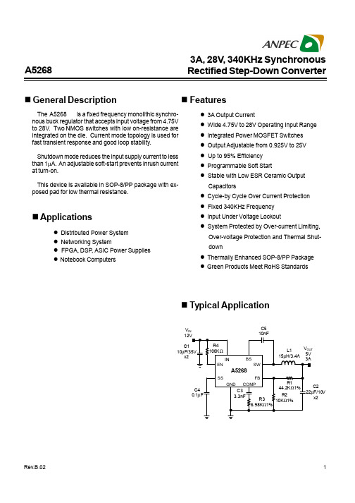
3A, 28V, 340KHz Synchronous Rectified Step-Down Converter
v
n Recommended Operating Conditions
Parameter
Ambient Temperature Range Junction Temperature Range Storage Temperature Range
Rating
-40 to +85 -40 to +125
EN BS SW
ie
C5 10nF VOUT 5V 3A
C1 10µ F/35V x2
L1 15µH/3.4A
A5268
SS GND FB S COMP
MDK-ARM - Release Notes

Release Notes forMicrocontroller Development KitThis file contains release notes and last m inute changes.Information in this file, the accompany manuals, and software isCopyright © 2014 ARM Ltd and ARM Germany GmbH.All rights reserved.Contents1. What's New in the Microcontroller Developm ent Kit2. Exam ple Program s3. Device Database™4. Peripheral Sim ulation5. Technical Support6. Contact DetailsThe Microcontroller Development Kit (MDK-ARM) supports software developm ent for and debugging of ARM7,ARM9, Cortex-M, and Cortex-R4 processor-based devices. A detailed description of MDK-ARM can be found in the section Complete User's Guide Selection of the µVision window Books. The Getting Started User's Guide is a good introduction to the m ain concepts of MDK-ARM and gives guidelines for program m ing ARM devices.What's New in the Microcontroller Development KitThe next sections list the changes for each release of the MDK-ARM toolset.Microcontroller Development Kit - Version 4.74[µVision]This MDK-ARM release is delivered with µVision V4.74.0.22 IDE.[Middleware][ARM Middleware][TCPnet]Corrected: corrected file upload failure in FTP client.[FlashFS]Corrected: the FAT file nam e processing in FlashFS (filenam es with leading '.' were not listed). Thelibrary version 4.74 includes the corrected FTP server interface module.Corrected: overlap bug in fcheck() function for EFS.[Segger Graphic Library]Updated: Segger emWin graphic library version 5.24b in folder ..\ARM\Segger\emWin\.[Device Simulation]Added: param eter -MULS to the Cortex-M0 sim ulator, which configures Multiplier Im plem entation type as"Small"(32-cycle iterative multiplier).Corrected: behaviour of sim ulation when executing DCW instruction.[Target debugging]Updated: Segger J-Link driver for ARM devices to version 4.76d.Updated: J-Link USB Driver Installer to support CDC.Updated: support for ST-Link USB-JTAG debugger. The ST-LINKIII-KEIL_SWO.dll MDK driver in folder..\ARM\STLink\ has been updated to version 2.0.5.0.[CMSIS]Updated to CMSIS 4.0 including:CMSIS-CORE3.30 (updated).CMSIS-DSP1.4.2 (updated).CMSIS-RTOS-API1.02.CMSIS-SVD1.1.[Board Support]NXP SemiconductorsAdded: Blinky and RTX_Blinky exam ples for MCB1500 starter kit, based on LPC1549 device.[New Supported Devices]AtmelSAMG51G18, SAMG51N18, SAMG53G19, SAMG53N19,SAM4CP16B, SAM4CMP16C CM4P0, SAM4CMP16C CM4P1, SAM4CMP8C CM4P0, SAM4CMP8C CM4P1,SAM4CMS16C CM4P0, SAM4CMS16C CM4P1, SAM4CMS8C CM4P0, SAM4CMS8C CM4P1,SAMD21E15A, SAMD21E16A, SAMD21E17A, SAMD21E18A,SAMD21G16A, SAMD21G17A, SAMD21G18A,SAMD21J16A, SAMD21J18A, SAMD21J16A,SAMR21E16A, SAMR21E17A, SAMR21E18A,SAMR21G16A, SAMR21G17A, and SAMR21G18A.CypressCY8C4013SXI-411, CY8C4013LQI-411, CY8C4013SXI-400, CY8C4013SXI-410,CY8C4014LQI-421, CY8C4014LQI-412, CY8C4014SXI-411, CY8C4014SXI-421,CY8C4014LQI-422, CY8C4014LQI-SLT1, and CY8C4014LQI-SLT2.Freescale SemiconductorSKEAZ128xxx4, SKEAZ64xxx4, SKEAZN8xxx4, SKEAZN16xxx2, SKEAZN32xxx2, SKEAZN64xxx2,MKE04Z8xxx4, MKE02Z16xxx2, MKE02Z32xxx2, and MKE02Z64xxx2.NXPLPC1517, LPC1518, LPC1519, LPC1547, LPC1548, and LPC1549.SpansionS6E1A11B0A, S6E1A11C0A, S6E1A12B0A, and S6E1A12C0A.STMicroelectronicsSTM32F401CD, STM32F401RD, STM32F401VD, STM32F401CE, STM32F401RE, STM32F401VE, andSTM32L162RD.Texas InstrumentsTM4C123GH6ZXR, TM4C1290NCPDT, TM4C1290NCZAD, TM4C1292NCPDT, TM4C1292NCZAD,TM4C1294KCPDT, TM4C1294NCPDT, TM4C1294NCZAD, TM4C1299KCZAD, TM4C129CNCPDT,TM4C129CNCZAD,TM4C129DNCPDT, TM4C129DNCZAD, TM4C129EKCPDT, TM4C129ENCPDT, TM4C129ENCZAD, andTM4C129XNCZAD.Microcontroller Development Kit - Version 4.73[µVision]This MDK-ARM release is delivered with µVision V4.73.0.0 IDE.Corrected: issue when pressing the F7-Key, which started a rebuild of the project. New: pressing the F7-key builds only the changed files.[Middleware][ARM Middleware][TCPnet]Added: user-configurable character encoding in HTTP Server service. The function http_encoding()optionally changes the default character encoding in the browser to support various national charactersets.Corrected: TCP socket closing problem in half-open connection state.[USB Device and USB Host]Corrected: USB Device audio library to support sam ples of size different then 2^n (in bytes).[Segger Graphic Library]Updated: Segger emWin graphic library version 5.22a in folder ..\ARM\Segger\emWin\.[New Supported Devices]AtmelSAM4LC8A, SAM4LC8B, SAM4LC8C, SAM4LS8A, SAM4LS8B, SAM4LS8C,SAM4S2A, SAM4S2B, SAM4S2C, SAM4S4A, SAM4S4B, and SAM4S4C.CypressCY8C4124AXI-443, CY8C4124LQI-443, CY8C4124PVI-432, CY8C4124PVI-442, CY8C4125AXI-473,CY8C4125AXI-483, CY8C4125LQI-483, CY8C4125PVI-482, CY8C4244AXI-443, CY8C4244LQI-443,CY8C4244PVI-432, CY8C4244PVI-442, CY8C4245AXI-473, CY8C4245AXI-483,CY8C4245LQI-483, and CY8C4245PVI-482.Energy MicroEFM32ZG108F4, EFM32ZG108F8, EFM32ZG108F16, EFM32ZG108F32,EFM32ZG110F4, EFM32ZG110F8, EFM32ZG110F16, EFM32ZG110F32,EFM32ZG210F4, EFM32ZG210F8, EFM32ZG210F16, EFM32ZG210F32,EFM32ZG222F4, EFM32ZG222F8, EFM32ZG222F16, and EFM32ZG222F32.Freescale SemiconductorMK24FN1M0xxx12, MK63FN1M0xxx12, MK64FN1M0xxx12, and MK64FX512xxx12.HoltekHT32F1655 and HT32F1656.InfineonXMC1100-8, XMC1100-16, XMC1100-32,XMC1201-16, XMC1201-32, XMC1201-64, XMC1201-200,XMC1202-16, XMC1202-32, XMC1301-8, XMC1301-16, XMC1301-32,XMC1302-8, XMC1302-16, XMC1302-32, and XMC1302-64.NXP (founded by Philips)LPC11E37/401, LPC1125, LPC4312, LPC4312 CM0, LPC4313, LPC4313 CM0, LPC4315,LPC4315 CM0, LPC4317, LPC4317 CM0, LPC4322, LPC4322 CM0,LPC4323, LPC4323 CM0, LPC4325, LPC4325 CM0, LPC4327,LPC4327 CM0, LPC4333, LPC4333 CM0, LPC4337, and LPC4337 CM0.SpansionMB9AF121K, MB9AF121L, MB9AF131M, MB9AF131N, MB9AF132M, MB9AF132N,MB9AF421K, MB9AF421L, MB9AFA41L, MB9AFA41M, MB9AFA41N,MB9AFA42L, MB9AFA42M, MB9AFA42N, MB9AFA44L, MB9AFA44M,MB9AFA44N, MB9BF102N, MB9BF102R, MB9BF112N, MB9BF114N,MB9BF115N, MB9BF116N, MB9BF128S, MB9BF128T, MB9BF129S,MB9BF129T, MB9BF166M, MB9BF166N, MB9BF166R, MB9BF167M,MB9BF167N, MB9BF167R, MB9BF168M, MB9BF168N, MB9BF168R,MB9BF328S, MB9BF328T, MB9BF329S, MB9BF329T, MB9BF366M,MB9BF366N, MB9BF366R, MB9BF367M, MB9BF367N, MB9BF367R,MB9BF368M, MB9BF368N, MB9BF368R, MB9BF412N, MB9BF414N, MB9BF415N,MB9BF416N, MB9BF428S, MB9BF428T, MB9BF429S, MB9BF429T,MB9BF466M, MB9BF466N, MB9BF466R, MB9BF467M, MB9BF467N, MB9BF467R,MB9BF468M, MB9BF468N, MB9BF468R, MB9BF528S, MB9BF528T, MB9BF529S,MB9BF529T, MB9BF566M, MB9BF566N, MB9BF566R,MB9BF567M, MB9BF567N, MB9BF567R,MB9BF568M, MB9BF568N, and MB9BF568R.STMicroelectronicsSTM32F030C6, STM32F030C8, STM32F030F4, STM32F030K6, STM32F030R8, STM32F401CB, STM32F401CC, STM32F401RB, STM32F401RC, STM32F401VB, STM32F401VC,STM32L100C6, STM32L100R8, STM32L100RB, STM32L100RC, STM32L151CC,STM32L151UC, STM32L152CC, STM32L162RC, STM32L162VC, STM32F071CB,STM32F071RB, STM32F071VB, STM32F072C8, STM32F072R8, STM32F072RB,STM32F072VB, STM32F078CB, STM32F078VB, STM32L151C6xxA, STM32L151C8xxA,STM32L151CBxxA, STM32L151R6xxA, STM32L151R8xxA, STM32L151RBxxA,STM32L151V8xxA, STM32L151VBxxA, STM32L152C6xxA, STM32L152C8xxA,STM32L152CBxxA, STM32L152R6xxA, STM32L152R8xxA, STM32L152RBxxA,STM32L152V8xxA, and STM32L152VBxxA.Texas InstrumentsCC2538NF11, CC2538NF23, CC2538NF53, CC2538SF23, CC2538SF53,TM4C1297NCZAD, TM4C1299NCZAD, and TM4C129LNCZAD.ToshibaTMPM462F10FG, TMPM462F10XBG, TMPM462F15FG, and TMPM462F15XBG.[Device Support]AtmelAdded: System Viewer file for SAM9M10 devices, in folder ..\ARM\SFD\Atmel\SAM9M10\.[CMSIS support]AtmelAdded: suppport for SAM4C devices, in folders ..\ARM\INC\Atmel\SAM4C\,..\ARM\Startup\Atmel\SAM4C\, and ..\ARM\SFD\Atmel\SAM4C\.Added: suppport for SAM4L8 devices, in folders ..\ARM\INC\Atmel\SAM4L\,..\ARM\Startup\Atmel\SAM4L\, and ..\ARM\SFD\Atmel\SAM4L\.CypressAdded: suppport for Cypress CY8C42xx devices, in folder ..\ARM\Startup\Cypress\.EnergyMicroAdded: suppport for EFM32ZG devices, in folders ..\ARM\INC\EnergyMicro\EFM32ZG\,..\ARM\Startup\EnergyMicro\EFM32ZG\, and ..\ARM\SFD\EnergyMicro\EFM32ZG\.Fujitsu SemiconductorAdded: suppport for MB9B520T devices, in folders ..\ARM\INC\Fujitsu\MB9B520T\,..\ARM\Startup\Fujitsu\MB9B520T\, and ..\ARM\SFD\Fujitsu\MB9B520T\.Added: suppport for MB9B420T devices, in folders ..\ARM\INC\Fujitsu\MB9B420T\,..\ARM\Startup\Fujitsu\MB9B420T\, and ..\ARM\SFD\Fujitsu\MB9B420T\.Added: suppport for MB9B320T devices, in folders ..\ARM\INC\Fujitsu\MB9B320T\,..\ARM\Startup\Fujitsu\MB9B320T\, and ..\ARM\SFD\Fujitsu\MB9B320T\.Added: suppport for MB9B120T devices, in folders ..\ARM\INC\Fujitsu\MB9B120T\,..\ARM\Startup\Fujitsu\MB9B120T\, and ..\ARM\SFD\Fujitsu\MB9B120T\.Added: suppport for MB9A420L devices, in folders ..\ARM\INC\Fujitsu\MB9A420L\,..\ARM\Startup\Fujitsu\MB9A420L\, and ..\ARM\SFD\Fujitsu\MB9A420L\.Added: suppport for MB9A120L devices, in folders ..\ARM\INC\Fujitsu\MB9A120L\,..\ARM\Startup\Fujitsu\MB9A120L\, and ..\ARM\SFD\Fujitsu\MB9A120L\.Added: suppport for MB9AA40NA devices, in folders ..\ARM\INC\Fujitsu\MB9AA40NA\,..\ARM\Startup\Fujitsu\MB9AA40NA\, and ..\ARM\SFD\Fujitsu\MB9AA40NA\.Added: suppport for MB9A130N devices, in folders ..\ARM\INC\Fujitsu\MB9A130N\,..\ARM\Startup\Fujitsu\MB9A130N\, and ..\ARM\SFD\Fujitsu\MB9A130N\.Added: suppport for MB9B410R devices, in folders ..\ARM\INC\Fujitsu\MB9B410R\,..\ARM\Startup\Fujitsu\MB9B410R\, and ..\ARM\SFD\Fujitsu\MB9B410R\.Added: suppport for MB9B110R devices, in folders ..\ARM\INC\Fujitsu\MB9B110R\,..\ARM\Startup\Fujitsu\MB9B110R\, and ..\ARM\SFD\Fujitsu\MB9B110R\.Added: suppport for MB9B160R devices, in folders ..\ARM\INC\Fujitsu\MB9B160R\,..\ARM\Startup\Fujitsu\MB9B160R\, and ..\ARM\SFD\Fujitsu\MB9B160R\.Added: suppport for MB9B360R devices, in folders ..\ARM\INC\Fujitsu\MB9B360R\,..\ARM\Startup\Fujitsu\MB9B360R\, and ..\ARM\SFD\Fujitsu\MB9B360R\.Added: suppport for MB9B460R devices, in folders ..\ARM\INC\Fujitsu\MB9B460R\,..\ARM\Startup\Fujitsu\MB9B460R\, and ..\ARM\SFD\Fujitsu\MB9B460R\.Added: suppport for MB9B560R devices, in folders ..\ARM\INC\Fujitsu\MB9B560R\,..\ARM\Startup\Fujitsu\MB9B560R\, and ..\ARM\SFD\Fujitsu\MB9B560R\.NXP (founded by Philips)Added: suppport for LPC112x devices, in folders ..\ARM\INC\NXP\LPC112x\,..\ARM\Startup\NXP\LPC112x \, and ..\ARM\SFD\NXP\LPC112x\.STMicroelectronicsAdded: suppport for STM32L1xx Value Line Devices devices, in folder..\ARM\SFD\ST\STM32L1xx\.Added: suppport for STM32F030 devices, in folders ..\ARM\Startup\ST\STM32F0xx\ and..\ARM\SFD\ST\STM32F0xx\.Texas InstrumentsAdded: suppport for TI CC2538 devices, in folder ..\ARM\SFD\TI\CC2538\.[Flash programming]AtmelAdded: ATSAM4L_512.FLM flash program m ing algorithm for Atmel SAM4L8 based devices in folder ..\ARM\Flash\.CypressAdded: CY8C42xx.FLM flash program m ing algorithm for Cypress CY8C42xx devices, in folder..\ARM\Flash\.Fujitsu SemiconductorAdded: MB9B560_1024.FLM and MB9B560_WORK32.FLM flash program m ing algorithm s for Fujitsu MB9B160R, MB9B360R, MB9B460R, and MB9B560R based devices in folder ..\ARM\Flash\.Added: MB9B520T_1024.FLM, MB9B520T_1536.FLM, and MB9B520T_ROM1.FLM flash program m ing algorithm s for Fujitsu MB9B120T based devices in folder ..\ARM\Flash\.Added: MB9A420L_64.FLM flash program m ing algorithm s for Fujitsu MB9A120L based devices in folder ..\ARM\Flash\.NXP (founded by Philips)Added: LPC18xx43xx_384_BA.FLM and LPC18xx43xx_384_BB.FLM flash program m ing algorithm for NXP KPC43xx devices, in folder ..\ARM\Flash\.STMicroelectronicsAdded: STM32F4xx_128.FLM and STM32F4xx_256.FLM flash program m ing algorithm s forSTM32F401 based devices in folder ..\ARM\Flash\.Added: STM32F0xx_128.FLM , STM32F0xx_64.FLM, STM32F0xx_32.FLM, andSTM32F0xx_16.FLM flash program m ing algorithm s for STM32F030 based devices in folder..\ARM\Flash\.[Board Support]AtmelAdded: Blinky, RTX_Blinky, and Bootloader exam ples for AT91SAM9M10-EK starter kit, based onAT91SAM9M10 device.EnergyMicroAdded: Blinky and RTX_Blinky exam ples for EFM32ZG_STK3200 starter kit, based on EFM32ZG222F32device.Added: Blinky and RTX_Blinky exam ples for EFM32LG_DK3650 board, based on EFM32LG990F256device.Added: Blinky and RTX_Blinky exam ples for EFM32WG_STK3800 board, based on EFM32WG990F256device.Freescale SemiconductorAdded: Blinky exam ple for FRDM-KE04Z starter kit, based on MKE04Z8xxx4 device.Added: Blinky, RTX_Blinky, FlexMem_Cfg, and ProgOnce_Cfg exam ples for FRDM-K20D50M evaluationboard, based on MK20DX128xxx5 device.STMicroelectronicsAdded: Blinky and RTX_Blinky exam ples for STM32L1-Discovery evaluation board, based onSTM32L100RC device.Added: Blinky and RTX_Blinky exam ples for STM32F030-Discovery evaluation board, based onSTM32F030R8 device.Added: Blinky_ULp exam ple for STM32303C-EVAL board, based on STM32F303VC device.[Target debugging]Updated: The CMSIS-DAP driver now supports the Micro Trace Buffer (MTB) of Cortex-M0+ devices.Updated: ULINK2 device firm ware to version 2.02. This version rem oves the Windows warning "This device can perform faster if connected to USB 2.0".Updated: Segger J-Link driver for ARM devices to version 4.76d.Microcontroller Development Kit - Version 4.72a[µVision]This MDK-ARM release is delivered with µVision V4.72.10.0 IDE. This version corrects build errors. Microcontroller Development Kit - Version 4.72[ARM Compiler]This version of MDK-ARM contains ARM Compiler 5.03u2.All com piler related files are located in ..\ARM\ARMCC\ directory.Details can be found in the Compiler specific Release Notes..[µVision]This MDK-ARM release is delivered with µVision V4.72.0.0 IDE.[uVision Debugger][Middleware][ARM Middleware][TCPnet]Added: support for user application notification in FTP Server service. An optional notification functionftp_evt_notify() m ay be used to receive notification of FTP server events, such as: user login, userlogout, file upload, file download, etc.Updated: handling of file write errors and data transfer aborts in FTP Server service. If a local filewrite error occurs, the service aborts file upload operation. Additionally, if the data connection isaborted, the service stops file download operation.Added: support for extended DHCP option 42 (NTP server list) in DHCP Client. An additionalconfiguration option NTP Servers in Net_Config.c is used to enable or disable this option.Added: com m and FTPC_CMD_NLIST in FTP Client service. This com m and lists only file nam es, without any additional file inform ation.Added: data transfer abort functionality in file retrieve operation of FTP Client service. The FTP client service now aborts data transfer, if a file write error occurs on local system.Corrected: potential dynam ic memory dead-lock, if HTTP server is serving large web resources.[USB Device and USB Host]ExamplesAdded: CDC exam ple for Infineon Hexagon Application Kit in folder..ARM\Boards\Infineon\Hexagon Application Kit\CPU_45A-V2\RL\USB\Device\CDC_ACM. [New Supported Devices]AtmelSAM4N16B, SAM4N16C, SAM4N8A, SAM4N8B, SAM4N8C,SAMD20E14, SAMD20E15, SAMD20E16, SAMD20E17, SAMD20G14, SAMD20G15,SAMD20G16, SAMD20G17, SAMD20G18, SAMD20J14,SAMD20J15, SAMD20J16, SAMD20J17, and SAMD20J18.CypressCY8C5265AXI-LP056, CY8C5265AXI-LP082, CY8C5265LTI-LP050, CY8C5265LTI-LP058, CY8C5266AXI-LP033, CY8C5266AXI-LP132, CY8C5266LTI-LP029, CY8C5266LTI-LP150, CY8C5267AXI-LP051, CY8C5267LTI-LP089, CY8C5268AXI-LP047, CY8C5268LTI-LP030, CY8C5465AXI-LP043, CY8C5465LTI-LP104, CY8C5466AXI-LP002, CY8C5466AXI-LP107, CY8C5466LTI-LP072, CY8C5466LTI-LP085, CY8C5467AXI-LP108, CY8C5467LTI-LP003, CY8C5468AXI-LP106, CY8C5468LTI-LP026, CY8C5666AXI-LP001, CY8C5666AXI-LP004, CY8C5666LTI-LP005, CY8C5667AXI-LP006, CY8C5667AXI-LP040, CY8C5667LTI-LP008, CY8C5667LTI-LP009, CY8C5667LTI-LP041, CY8C5668AXI-LP010, CY8C5668AXI-LP013, CY8C5668AXI-LP034, CY8C5668LTI-LP014, CY8C5866AXI-LP020, CY8C5866AXI-LP021, CY8C5866LTI-LP022, CY8C5867AXI-LP023, CY8C5867AXI-LP024, CY8C5867LTI-LP025, CY8C5867LTI-LP028, CY8C5868AXI-LP031, CY8C5868AXI-LP032, CY8C5868AXI-LP035, CY8C5868LTI-LP036, CY8C5868LTI-LP038, and CY8C5868LTI-LP039.EnergyMicroEFM32WG230F128, EFM32WG230F256, EFM32WG230F64, EFM32WG232F128, EFM32WG232F256,EFM32WG232F64,EFM32WG280F128, EFM32WG280F256, EFM32WG280F64, EFM32WG290F128, EFM32WG290F256,EFM32WG290F64,EFM32WG295F128, EFM32WG295F256, EFM32WG295F64, EFM32WG330F128, EFM32WG330F256,EFM32WG330F64,EFM32WG332F128, EFM32WG332F256, EFM32WG332F64, EFM32WG380F128, EFM32WG380F256,EFM32WG380F64,EFM32WG390F128, EFM32WG390F256, EFM32WG390F64, EFM32WG395F128, EFM32WG395F256,EFM32WG395F64,EFM32WG840F128, EFM32WG840F256, EFM32WG840F64, EFM32WG842F128, EFM32WG842F256,EFM32WG842F64,EFM32WG880F128, EFM32WG880F256, EFM32WG880F64, EFM32WG890F128, EFM32WG890F256,EFM32WG890F64,EFM32WG895F128, EFM32WG895F256, EFM32WG895F64, EFM32WG940F128, EFM32WG940F256,EFM32WG940F64,EFM32WG942F128, EFM32WG942F256, EFM32WG942F64, EFM32WG980F128, EFM32WG980F256,EFM32WG980F64, EFM32WG990F128, EFM32WG990F256, EFM32WG990F64, EFM32WG995F128,EFM32WG995F256, and EFM32WG995F64.Freescale SemiconductorMKE02Z16xxx2, MKE02Z32xxx2, MKE02Z64xxx2, MKE04Z8xxx4,Fujitsu SemiconductorMB9AF141L, MB9AF141M, MB9AF141N, MB9AF142L, MB9AF142M,MB9AF142N, MB9AF144L, MB9AF144M, and MB9AF144N.NuvotonM0516LBN, M0516ZBN, M052LBN, M052ZBN, M054LBN,M054ZBN, M058LBN, M058SLAN, M058SSAN, M058SZAN,M058ZBN, MINI51TAN, MINI52TAN, MINI54TAN,NUC123SC2AN1, NUC123LC2AN1, NUC123ZC2AN1, NUC123SD4AN0, NUC123LD4AN0,NUC123ZD4AN0, NUC140VE3CN, NUC140RE3CN, NUC140RD2CN, NUC140RC1CN,NUC140LE3CN, NUC140LD2CN, NUC140LC1CN, NUC130VE3CN, NUC130RE3CN,NUC130RD2CN, NUC130RC1CN, NUC130LE3CN, NUC130LD2CN, NUC130LC1CN,NUC120RD2BN, NUC120RD1BN, NUC120RC1BN, NUC120LD2BN, NUC120LD1BN,NUC120LC1BN, NUC100RD2BN, NUC100RD1BN, NUC100RC1BN, NUC100LD2BN, NUC100LD1BN, NUC100LC1BN, NUC220VE3AN, NUC220SE3AN, NUC220LE3AN, NUC220SD2AN, NUC220LD2AN, NUC220SC2AN, NUC220LC2AN, NUC200VE3AN, NUC200SE3AN, NUC200LE3AN, NUC200SD2AN, NUC200LD2AN, NUC200SC2AN, NUC200LC2AN, NANO100KE3BN, NANO100SE3BN, NANO100KD3BN, NANO100SD3BN, NANO100LD3BN, NANO100KD2BN, NANO100SD2BN, NANO100LD2BN, NANO100KC2BN, NANO100LC2BN, NANO100LE3BN, NANO100SC2BN, NANO110KE3BN, NANO110SE3BN, NANO110KD3BN, NANO110SD3BN, NANO110KD2BN,NANO110SD2BN, NANO110KC2BN, NANO110SC2BN,NANO120KE3BN, NANO120SE3BN, NANO120LE3BN, NANO120KD3BN, NANO120SD3BN, NANO120LD3BN,NANO120KD2BN, NANO120SD2BN, NANO120LD2BN, NANO120KC2BN, NANO120SC2BN, NANO120LC2BN, NANO130KE3BN, NANO130SE3BN, NANO130KD3BN, NANO130SD3BN,NANO130KD2BN, NANO130SD2BN, NANO130KC2BN, NANO130SC2BN,NXP (founded by Philips)LPC4310 CM0, LPC4320 CM0, LPC4330 CM0, LPC4350 CM0, LPC4353 CM0, and LPC4357 CM0.STMicroelectronicsSTM32F429BG, STM32F429BI, STM32F429IG, STM32F429II, STM32F429NG,STM32F429NI, STM32F429VG, STM32F429VI, STM32F429ZG, STM32F429ZI,STM32F439BG, STM32F439BI, STM32F439IG, STM32F439II, STM32F439NG,STM32F439NI, STM32F439VG, STM32F439VI, STM32F439ZG, and STM32F439ZI.Texas InstrumentsTM4C1290NCPDT, TM4C1290NCZAD, TM4C1292NCPDT, TM4C1292NCZAD, TM4C1294NCPDT,TM4C1294NCZAD, TM4C129CNCPDT, TM4C129CNCZAD, TM4C129DNCPDT, TM4C129DNCZAD,TM4C129ENCPDT, TM4C129ENCZAD, TM4C129XNCZAD, TM4E129BNCZAD, TM4E129SNCZAD,TM4E129XNCZAD, TMPM343F10XBG, TMPM343FDXBG, and TMPM343FEXBG.[Device Support][CMSIS support]AtmelAdded: suppport for Atmel SAMD20 devices, in folders ..\ARM\INC\Atmel\SAMD20\,..\ARM\Startup\Atmel\SAMD20\, and ..\ARM\SFD\Atmel\SAMD20\.Added: suppport for Atmel SAM4N devices, in folders ..\ARM\INC\Atmel\SAM4N\,..\ARM\Startup\Atmel\SAM4N\, and ..\ARM\SFD\Atmel\SAM4N\.EnergyMicroAdded: suppport for EnergyMicro Wonder Gecko devices, in folders..\ARM\INC\EnergyMicro\EFM32WG\, ..\ARM\Startup\EnergyMicro\EFM32WG\, and..\ARM\SFD\EnergyMicro\EFM32WG\.Freescale SemiconductorAdded: suppport for Kinetis KE02 devices, in folders ..\ARM\INC\Freescale\Kinetis\,..\ARM\Startup\Freescale\Kinetis\, and ..\ARM\SFD\Freescale\Kinetis\.Added: suppport for Kinetis KE04 devices, in folders ..\ARM\INC\Freescale\Kinetis\,..\ARM\Startup\Freescale\Kinetis\, and ..\ARM\SFD\Freescale\Kinetis\.Fujitsu SemiconductorAdded: suppport for MB9A140N devices, in folders ..\ARM\INC\Fujitsu\MB9A140N\,..\ARM\Startup\Fujitsu\MB9A140N\, and ..\ARM\SFD\Fujitsu\MB9A140N\.NuvotonAdded: suppport for NUC123Series devices, in folders ..\ARM\INC\Nuvoton\NUC123Series\,..\ARM\Startup\Nuvoton\NUC123Series\, and ..\ARM\SFD\Nuvoton\NUC123Series\.Added: suppport for NUC200Series devices, in folders ..\ARM\INC\Nuvoton\NUC200Series\,..\ARM\Startup\Nuvoton\NUC200Series\, and ..\ARM\SFD\Nuvoton\NUC200Series\.Added: suppport for Nano1xx devices, in folders ..\ARM\INC\Nuvoton\Nano1xx\,..\ARM\Startup\Nuvoton\Nano1xx\, and ..\ARM\SFD\Nuvoton\Nano1xx\.SONiXAdded: suppport for SN32F100 based devices, in folders ..\ARM\INC\SONiX\SN32F100\,..\ARM\Startup\SONiX\SN32F100\, and ..\ARM\SFD\SONiX\SN32F100\.Added: suppport for SN32F110 based devices, in folders ..\ARM\INC\SONiX\SN32F110\,..\ARM\Startup\SONiX\SN32F110\, and ..\ARM\SFD\SONiX\SN32F110\.STMicroelectronicsAdded: suppport for STM32F4xx based devices, in folders ..\ARM\INC\ST\STM32F4xx\,..\ARM\Startup\ST\STM32F4xx\, and ..\ARM\SFD\ST\STM32F4xx\.Texas InstrumentsAdded: suppport for TM4C123 based devices, in folders ..\ARM\INC\TI\TM4C123\,..\ARM\Startup\TI\TM4C123\, and ..\ARM\SFD\TI\TM4C123\.Added: suppport for TM4C129 based devices, in folders ..\ARM\INC\TI\TM4C129\,..\ARM\Startup\TI\TM4C129\, and ..\ARM\SFD\TI\TM4C129\.Added: suppport for TM4E129 based devices, in folders ..\ARM\INC\TI\TM4E129 \,..\ARM\Startup\TI\TM4E129\, and ..\ARM\SFD\TI\TM4E129\.[Flash programming]AtmelAdded: ATSAMD20_16.FLM, ATSAMD20_32.FLM, ATSAMD20_64.FLM, ATSAMD20_128.FLM, and ATSAMD20_256.FLM flash program m ing algorithm s for Atmel ATSAM20D based devices in folder..\ARM\Falsh\.Added: ATSAM4N_512.FLM and ATSAM4N_1024.FLM flash program m ing algorithm s for AtmelATSAM4N based devices in folder ..\ARM\Falsh\.Freescale SemiconductorAdded: MKE02Zxxx_EE256B.FLM, MKE02Zxxx_P16KB.FLM, MKE02Zxxx_P32KB.FLM, andMKE02Zxxx_P64KB.FLM flash program m ing algorithm s for Kinetis KE02 based devices in folder..\ARM\Flash\.Added: MKE04Zxxx_P8KB.FLM flash program m ing algorithm s for Kinetis KE04 based devices in folder..\ARM\Flash\.NuvotonAdded: NUC2xx_CFG.FLM, NUC2xx_AP_128.FLM, NUC2xx_AP_64.FLM, NUC2xx_AP_32.FLM,NUC2xx_LD_4.FLM, and NUC2xx_DAT.FLM flash program m ing algorithm s for NUC200Series devicesin folder ..\ARM\Flash\.Added: Nano100_CFG.FLM, Nano100_AP_123.FLM, Nano100_DAT.FLM, Nano100_AP_64.FLM,Nano100_LD_4.FLM, and Nano100_AP_32.FLM flash program m ing algorithm s for Nano1xx baseddevices in folder ..\ARM\Flash\.SONiXAdded: SN32F100_64.FLM and SN32F110_64.FLM flash program m ing algorithm s for SN32F100 andSN32F110 based devices in folder ..\ARM\Flash\.[Board Support]AtmelAdded: Blinky and RTX_Blinky exam ples for SAMD20-XPRO board, based on SAMD20J18 device.SONiXAdded: Hello exam ple for SN32F100_Starter_Kit board, based on SN32F109 device.STMicroelectronicsAdded: Blinky and RTX_Blinky exam ples for STM324x9I-EVAL evaluation board, based on STM32F439NIdevice.Added: Blinky, RTX_Blinky, and Blinky_ULp for STM32437I-EVAL evaluation board, based onSTM32F437II device.[Target debugging]Updated: support for NULink debugger from Nuvoton. The Nu_Link.dll driver dll in folder ..\ARM\NULInk\ has been updated to version 1.2.1.0.Updated: debug driver lm idk-agdi.dll for TI Stellaris In-Ciruit debug interface to version 211.0.0.0 in folder..\ARM\BIN\.Microcontroller Development Kit - Version 4.71a[uVision Debugger]Corrected: Missing RTX views for Cortex-M targets.[New Supported Devices]SONiXSN32F107, SN32F108, SN32F109,SN32F117, SN32F118, and SN32F119.Microcontroller Development Kit - Version 4.71[ARM Compiler]This version of MDK-ARM contains ARM Compiler 5.03u1.All com piler related files are located in ..\ARM\ARMCC\ directory.Details can be found in the Compiler specific Release Notes..[CMSIS]Updated: version 3.20.The software portions that are deployed in the application program are now under a BSD license which allows usage of CMSIS com ponents in any com m ercial or open source projects. The individual com ponents have been updated as listed below:CMSIS-CORE adds functions for setting breakpoints, supports the latest GCC Compiler, and containsseveral corrections.CMSIS-DSP library is optim ized for m ore perform ance and contains several bug fixes.CMSIS-RTOS API is extended with capabilities for short tim eouts, Kernel initialization, and prepared for a C++ interface.CMSIS-SVD is unchanged.[µVision]This MDK-ARM release is delivered with µVision V4.71.0 IDE.Enhanced:Automatic Code Completion and Parameter Information.Enhanced: Dynamic Syntax Checking.[uVision Debugger]The uVision debugger now shows device specific interrupt nam es if defined in a System Viewer Description (SVD) file.The tim e window lim itation of 10 m s has been rem oved for searching and saving trace data in Unlimited Trace m ode.Updated: Segger J-Link driver for ARM devices to version 4.68a.[Middleware][ARM Middleware][TCPnet]Added: SNTP client im plem entation with support for unicast and broadcast m ode.Corrected: buffer queue clearing in BSD socket interface, which m ight cause early receive data loss in listening server sockets.Corrected: potential data loss in BSD socket receive, if the system runs out of m em ory.ExamplesAdded: BSD_client, BSD_server, DNS_dem o, FTP_dem o, Http_dem o, Http_upload, LEDClient,LEDSwitch, SMTP_dem o, SNMP_dem o, and Telnet_dem o exam ples for TWR-K60D100M evaluationboard in folder ..\Boards\Freescale\TWR-K60D100M\RL\TCPnet\ based on MK60DN512xxx10device.[FlashFS]ExamplesAdded: SD_File exam ple for TWR-K60D100M evaluation board in folder ..\Boards\Freescale\TWR-K60D100M\RL\FlashFS\ based on MK60DN512xxx10 device.[USB Device and USB Host]ExamplesAdded: HID and Mem ory exam ples for TWR-K60D100M evaluation board in folder..\Boards\Freescale\TWR-K60D100M\RL\USB\Device\ based on MK60DN512xxx10 device.Added: RTX HID and RTX Mem ory exam ples for TWR-K60D100M evaluation board in folder..\Boards\Freescale\TWR-K60D100M\RL\USB\Device\RTX\ based on MK60DN512xxx10 device.Added: HID_Kbd and MSD_File exam ples for TWR-K60D100M evaluation board in folder..\Boards\Freescale\TWR-K60D100M\RL\USB\Host\ based on MK60DN512xxx10 device.[CAN]ExamplesAdded: CAN_Ex1 and CAN_Ex1 exam ples for TWR-K60D100M evaluation board in folder..\Boards\Freescale\TWR-K60D100M\RL\CAN\ based on MK60DN512xxx10 device.[Segger Graphic Library]Updated: Segger emWin graphic library version 5.20b in folder ..\ARM\Segger\emWin\.[New Supported Devices]AtmelSAM3N00A, SAM3N00B, SAM3N0A, SAM3N0B, SAM3N0C,SAM4E16C, SAM4E16E, SAM4E8C, SAM4E8E,SAM4SA16B, SAM4SA16C, SAM4SD16B, SAM4SD16C, SAM4SD32B, and SAM4SD32C.Dialog SemiconductorDA14580.Freescale SemiconductorMK21FN1M0xxx12, MK21FX512xxx12, MK22FN1M0xxx12, MK22FX512xxx12,MKL02Z16xxx4, MKL02Z32xxx4, MKL02Z8xxx4, MKL16Z256xxx4,MKL26Z128xxx4, MKL26Z256xxx4, MKL34Z64xxx4, MKL36Z128xxx4,MKL36Z256xxx4, MKL46Z128xxx4, MKL46Z256xxx4, MKM13Z64xxx5,MKM14Z128xxx5, MKM14Z64xxx5, MKM32Z64xxx5, MKM33Z128xxx5,MKM33Z64xxx5, MKM34Z128xxx5, and MKM38Z128xxx5.。
瑞萨32位机 RX62T常见问题与解决办法
在100 MHz的频率下运行时,MCU仅消耗50mA的电流
●根据具体情况,可选择低功耗模式。
(休眠,所有模块停止,软件待机、深度软件待机)
[2012-3-29 10:51:59]
[问:cccfeb]
RX62T驱动电机的电路图有没有?有没有实例在网站上!
目前RX62T的产品实例还没有,客户基本上用H8/3062的老型号在做,如果能换成RX62T效果肯定明显,因为RX62T的性能比H8/3062高了很多.
[2012-3-29 10:51:57]
[问:liang-1011]
RX62T,32bitMCU的主要特点及优势?
[答:Kenwong]
增强型定时器(提高了PWM分辨率,带有比较器的启动定时器)
[答:tonyliu]
1.注意功率器件的选取。2.注意开关频率,通常开关频率越高,效率会有提高。
[2012-3-29 10:47:04]
[主持人:ChinaECNet]
各位网友,本次座谈的演示及问答内容,将于今天下午开始在中电网进行回放,同时还提供本次座谈的PPT内容下载,请大家关注中电网的更新。
[2012-3-29 10:47:52]
[2012-3-29 10:34:16]
[问:zpjnear]
请问光伏并网逆变器,光伏扬水逆变器,光伏微网逆变器中分别使用哪款MCU(Renesas)比较合适?
[答:Kenwong]
RX62T
[2012-3-29 10:34:44]
[问:ezcui]
在光伏逆变器上应用的单片机是否需有哪些严格或特殊的要求?
[2012-3-29 10:56:34]
基于LMX2594的K波段频率源的设计与实现

基于LMX2594的K波段频率源的设计与实现胡格;王志鹏;文继国【摘要】介绍了一种K波段频率源的设计方法.本文采用LMX2594数字锁相环芯片,并用C8051F330单片机对锁相环芯片进行操作,然后再倍频的方法实现了实现了该K波段频率源的设计.该频率源具有频率稳定度高,相位噪声低,杂散低等优点.测试结果表明该频率源的相位噪声为-90dBc@1kHz,-98dBc@10kHz;输出功率大于10dBm,可以满足系统的各项要求.【期刊名称】《电子世界》【年(卷),期】2018(000)017【总页数】3页(P119-121)【关键词】K波段;频率源;锁相环;相位噪声;杂散【作者】胡格;王志鹏;文继国【作者单位】成都信息工程大学;成都信息工程大学;成都信息工程大学【正文语种】中文1 引言频率源是现代微波通信系统的重要功能单元,在收发射机、雷达、通信、电子对抗和检测仪器等电子设备中被广泛应用,它的性能直接影响整个通信系统的性能[1]。
随着雷达等信息技术的发展,对频率源的稳定性、相位噪声、杂散和体积等性能指标提出了越来越高的要求[2]。
频率源的设计方法有直接频率合成、锁相环频率合成、直接数字频率合成、PLL+DDS频率合成[3-4]。
本文所设计与实现的点频源是通过采用锁相环频率合成技术产生一个点频率然后放大再通过倍频,最后滤波得到我们最终所需的信号。
图1 LMX2594功能框图2 锁相环的工作原理LMX2594是德州仪器生产的一款较高性能的宽带合成器,能产生10MHz至15GHz 范围内的任何频率,其显著特点是实现非常低的带内噪声和集成抖动。
高速N分频器没有预分频器,能够有效减少杂散的数量和振幅。
还有一个可减轻整数边界杂散的可编程输入乘法器。
LMX2594可以是单端输入输出,也可以是差分输入输出。
参考信号先由管脚 OSCINM 或 OSCINP 进入芯片,经过倍频,R分频器,然后再送到鉴相器。
鉴相器的输出经过电荷泵后由管脚CPOUT 输出至外部的环路滤波器,滤波后再经过管脚VTUNE来控制VCO,VCO信号经过一个可编程的N分频器来控制需要的频率,最后通过RFOUT输出。
MAX2870中文规格书

PARAMETER
CONDITIONS
REFERENCE OSCILLATOR INPUT (REF_IN)
REF_IN Input Frequency Range
REF_IN Input Sensitivity
REF_IN Input Capacitance
REF_IN Input Current
CONDITIONS
CP[3:0] = 1111, RSET = 5.1kI CP[3:0] = 0000, RSET = 5.1kI
With output dividers (1/2/4/8/16/32/64/128)
Open loop Open loop into 2:1 VSWR Fundamental VCO output Fundamental VCO output VCO output divided-by-2 VCO output divided-by-2
定购信息在数据资料的最后给出。 典型应用电路在数据手资料的最后给出。
相关型号以及配合该器件使用的推荐产品,请参见:china.maximintegrated. com/MAX2870.related。
功能框图
MAX2870
REF_IN
CLK DATA
LE
MUX
R COUNTER
X2
SPI AND REGISTERS
Both channels enabled, maximum output power
Total, including RFOUT, both channel (Note 3)
Each output divide-by-2 ICCVCO + ICCRF (Note 3) Low-power sleep mode
MSP430F5529实验指导书V1.0
MSP430F5529 实验指导书(V1.0)2014年10月27日东北林业大学机电工程学院“3+1”实验室实验一基础GPIO实验实验二键盘与液晶显示实验实验三时钟系统配置实验实验四看门狗与定时器实验实验五 AD/DA实验实验六比较器实验实验七 Flash实验实验八串行通信实验实验一基础GPIO实验【实验目的】1、熟悉CCS的基本使用方法;2、掌握MSP430系列单片机程序开发的基本步骤;3、掌握MSP430 IO口的基本功能。
【实验仪器】1、SEED-EXP430F5529v1.0开发板一套;2、PC机操作系统Windows XP或Windows 7,CCSv5.1集成开发环境。
【实验原理】CCS(Code Composer Studio)是 TI 公司研发的一款具有环境配置、源文件编辑、程序调试、跟踪和分析等功能的集成开发环境,能够帮助用户在一个软件环境下完成编辑、编译、链接、调试和数据分析等工作。
CCSv5.1 为 CCS 软件的最新版本,功能更强大、性能更稳定、可用性更高,是 MSP430 软件开发的理想工具。
SEED-EXP430F5529v1.0开发板上的有8个可操作的LED灯,与MCU的IO口对应关系如图1-1所示:图1-1 LED与MCU的IO对应关系电路我们可以通过控制单片机IO口的输出电平状态来控制各个LED灯的亮灭。
开发板上还有2个可操作的按键S1,S2。
如图1-2所示。
图1-2 按键电路我们可以通过读取与按键相连的IO口的输入电平状态来执行相应的操作。
此外,S1,S2还可以作为外部中断源,触发中断。
【实验内容】1、用调用头文件的方法,使能MSP430F5529开发板上的8个LED灯依次按顺序循环点亮;2、用按键S1控制开发板上LED1的亮灭状态(查询法);3、用按键S2控制开发板上跑马灯的循环速度(中断方式)。
【实验步骤】内容1:使能开发板上的8个LED灯依次按顺序循环点亮1、打开CCSv5并确定工作区间,然后选择File-->New-->CCS Project 弹出图1-3对话框。
嵌入式开发实验手册
嵌入式系统原理与应用实验栗华编着山东大学信息科学与工程学院二零一四年三月目录第一章实验硬件平台1.1北京博创UP-TECH三合一实验箱简介本实验指导书所依赖的硬件平台为北京博创兴盛科技有限公司生产的一种ARM9/Xscale经典三核心教学科研平台(型号:UP-TECHS2410/S2440/P270),本平台兼容PXA270核心CPU及S3C2410、S2440核心CPU的全部功能,是北京博创多年来嵌入式教学产品开发经验的结晶。
这里选配的是S3C2440核心板。
图1-1UP-CUP三合一实验箱外观应用案例:※支持Linux、WinCE、Vxworks、μC/OS-Ⅱ4套操作系统;※核心板可更换,同时拥有ARM9(S3C2410和S3C2440)和XScale(PXA270);※中国电子学会嵌入式工程师认证考试和师资培训指定平台;硬件资源:软件资源结构说明图1-2UP-TECH三合一实验箱实物结构图1-2UP-TECH三合一实验箱框图结构图1-3UP-TECH三合一实验箱框图结构版图1.2跳线设置参考说明:◆PCB上所有“EXPORT”丝印字符表示168Pin扩展槽◆JP1401RESET-SEL:设置复位电路,位置JTAG20插座下方。
1-2:ICE的ICE-TRST复位信号可以控制系统复位信号RESET。
2-3:ICE的ICE-TRST复位信号不可以控制系统复位信号RESET。
◆JP1402JTAGSEL:选择JTAG电路,位置JTAG20插座下方。
1-2:使能板载的UP-LINKJTAG电路。
2-3:使用外部的JTAG电缆或者ARMICE仿真器。
◆JP1103TXD1-SEL◆JP1104RXD1-SEL:UART1选择扩展槽或者RS232的DB9插座。
1-2:UART1连接RS232-1,从DB9串口插座输出。
2-3:UART1连接到扩展槽。
◆JP1101TXD2-SEL◆JP1102RXD2-SEL:UART2选择跳线,分别为RS485、IrDA、扩展槽1-2:UART2连接到RS485总线上。
IRS20957S IR
IRS20954S
Protected Digital Audio Driver
Features
• • • • • • • • Floating PWM input enables easy half bridge implementation Integrated programmable bi-directional over-current protection with self-reset function Programmable compensated preset deadtime for improved THD performances High noise immunity ±100 V high voltage ratings deliver up to 500 W output power 3.3 V / 5 V logic compatible input Operates up to 800 kHz RoHS compliant
Symbol
VB VS IDDZ VSS VHO VCC VLO VIN VCSD VDT IOREF VOCSET
Definition
High-side floating supply absolute voltage High-side floating supply offset voltage Floating input supply Zener clamp current Floating input supply absolute voltage High-side floating output voltage Low-side fixed supply voltage Low-side output voltage PWM input voltage CSD pin input voltage DT pin input voltage Reference output current to COM (Note 2) OCSET pin input voltage
DSP问题
DSP与单片机的区别作者: lilac | 浏览数(2480) | 评论数(0) | 2007-05-111、DSP的程序一般在RAM里运行,单片机的程序一般在flash或者rom里运行,因为dsp 的速度高,一般要100M以上,flash的速度达不到那么快;2、由于DSP的程序一般在RAM里执行,而脱机程序必须存储在ROM里以便掉电后不丢失,所以需要在上电后把程序从ROM搬到RAM里。
因此一些DSP在片内ROM里固化了一段程序来做这个工作,这段程序就称为bootloader;3、DSP的内核结构要较单片机复杂(这里说内核是因为现在的芯片都SOC化,很多单片机内核并不复杂,但加了很多片上外设也复杂了),针对信号处理做了硬件上的支持,如FIR、MAC、乘方、开方等;例如:典型的ARM核3万门,典型的51核1万门,而典型的DSP 核xx门(呵呵,这个有待补充);4、串行接口方式DSP多采用同步口,而单片机多采用异步口,DSP的同步串行口占用较少的CPU负荷,并且支持的速度更高;做DSP最应该懂得157个问题(转载)做DSP最应该懂得157个问题(转载)二.DSP的C语言同主机C语言的主要区别?1)DSP的C语言是标准的ANSI C,它不包括同外设联系的扩展部分,如屏幕绘图等。
但在CCS中,为了方便调试,可以将数据通过prinf命令虚拟输出到主机的屏幕上。
2)DSP的C语言的编译过程为,C编译为ASM,再由ASM编译为OBJ。
因此C和ASM的对应关系非常明确,非常便于人工优化。
3)DSP的代码需要绝对定位;主机的C的代码有操作系统定位。
4)DSP的C的效率较高,非常适合于嵌入系统。
三.DSP发展动态1.TMS320C2000 TMS320C2000系列包括C24x和C28x系列。
C24x系列建议使用LF24xx 系列替代C24x系列,LF24xx系列的价格比C24x便宜,性能高于C24x,而且LF24xxA具有加密功能。
LM5001MA中文资料
August 2007 LM5001High Voltage Switch Mode RegulatorGeneral DescriptionThe LM5001 high voltage switch mode regulator features all of the functions necessary to implement efficient high voltage Boost, Flyback, SEPIC and Forward converters, using few external components. This easy to use regulator integrates a 75 Volt N-Channel MOSFET with a 1 Amp peak current limit. Current mode control provides inherently simple loop com-pensation and line-voltage feed-forward for superior rejection of input transients. The switching frequency is set with a single resistor and is programmable up to 1.5MHz. The oscillator can also be synchronized to an external clock. Additional pro-tection features include: current limit, thermal shutdown, un-der-voltage lockout and remote shutdown capability. The device is available in both SO-8 and LLP-8 packages.Features■Integrated 75 volt N-Channel MOSFET■Ultra-wide input voltage range from 3.1V to 75V■Integrated high voltage bias regulator■Adjustable output voltage■ 1.5% output voltage accuracy■Current mode control with selectable compensation ■Wide bandwidth error amplifier■Integrated current sensing and limiting■Integrated slope compensation■85% maximum duty cycle limit■Single resistor oscillator programming■Oscillator synchronization capability■Enable / Undervoltage Lockout (UVLO) pin■Thermal shutdownPackages■SO-8■LLP-8 (4mm x 4mm)Typical Application Circuit20215701Boost Regulator Application Schematic© 2007 National Semiconductor LM5001 High Voltage Switch Mode RegulatorConnection DiagramsTop View SO-8 Package20215702Top View LLP-8 Package20215703Ordering InformationOrder Number Package TypeNSC Package DrawingSupplied As LM5001MA SO-8M08A 95 Units in a Rail LM5001MAX SO-8M08A 2500 Units on Tape and Reel LM5001SD LLP-8SDC08A 1000 Units on Tape and Reel LM5001SDX LLP-8SDC08A 4500 Units on Tape and Reel LM5001SDELLP-8SDC08A250 Units on Tape and ReelPin DescriptionsPin Name Description Application InformationSO LLP 13SW Switch pin The drain terminal of the internal power MOSFET.24VIN Input supply pinNominal operating range: 3.1V to 75V.35VCCBias regulator output, or input for external bias supply VCC tracks VIN up to 6.9V. Above VIN = 6.9V, VCC is regulated to 6.9 Volts. A 0.47 µF or greater ceramicdecoupling capacitor is required. An external voltage (7V –12V) can be applied to this pin which disables the internal VCC regulator to reduce internal power dissipation and improve converter efficiency.46GND GroundInternal reference for the regulator control functions and the power MOSFET current sense resistor connection.57RTOscillator frequency programming and optional synchronization pulse inputThe internal oscillator is set with a resistor, between this pin and the GND pin. The recommended frequency range is 50KHz to 1.5 MHz. The RT pin can accept synchronization pulses from an external clock. A 100 pF capacitor isrecommended for coupling the synchronizing clock to the RT pin.68FBFeedback input from the regulated output voltage This pin is connected to the inverting input of the internal error amplifier. The 1.26V reference is internally connectedto the non-inverting input of the error amplifier.71COMPOpen drain output of the internal error amplifierThe loop compensation network should be connected between the COMP pin and the FB pin. COMP pull-up is provided by an internal 5 k Ω resistor which may be used to bias an opto-coupler transistor (while FB is grounded) for isolated ground applications. 2L M 5001PinName Description Application Information SO LLP82EN Enable / Under Voltage Lock-Out /Shutdown input An external voltage divider can be used to set the line undervoltage lockout threshold. If the EN pin is left unconnected, a 6 µA pull-up current source pulls the EN pin high to enable the regulator.NA EP EP Exposed Pad, LLP only Exposed metal pad on the underside of the package with aresistive connection to pin 6. It is recommended to connectthis pad to the PC board ground plane in order to improveheat dissipation.LM5001Absolute Maximum Ratings (Note 1)If Military/Aerospace specified devices are required,please contact the National Semiconductor Sales Office/Distributors for availability and specifications.VIN to GND76VSW to GND (Steady State)-0.3V to 76VVCC, EN to GND14VCOMP, FB, RT to GND-0.3V to 7VMaximum Junction Temperature150°CStorage Temperature −65°C to +150°CESD Rating (Note 2) Human Body Model 2kVOperating ConditionsVIN3.1V to 75V Operating Junction Temperature−40°C to +125°CElectrical CharacteristicsLimits in standard type are for T J = 25°C only; limits in boldface type apply over thejunction temperature (T J ) range of -40°C to +125°C. Minimum and Maximum limits are guaranteed through test, design, or statistical correlation. Typical values represent the most likely parametric norm at T J = 25°C, and are provided for reference purposes only.V VIN = 10V, R RT = 48.7k Ω unless otherwise stated. See (Note 3).Symbol ParameterConditions Min Typ Max Units STARTUP REGULATORV VCC-REGVCC Regulator Output6.55 6.857.15V VCC Current Limit V VCC = 6V 1520 mA VCC UVLO Threshold V VCC increasing 2.6 2.83V VCC Undervoltage Hysteresis0.1 V Bias Current (I IN )V FB = 1.5V 3.1 4.5mA I QShutdown Current (I IN )V EN = 0V95130µAEN THRESHOLDSEN Shutdown Threshold V EN increasing 0.250.450.65V EN Shutdown Hysteresis0.1 V EN Standby Threshold V EN increasing 1.2 1.26 1.32V EN Standby Hysteresis 0.1 V EN Current Source 6 µA MOSFET CHARACTERISTICSMOSFET R DS(ON) plus Current Sense Resistance I D = 0.5A 490800m Ω MOSFET Leakage Current V SW = 75V 0.055µAMOSFET Gate ChargeV VCC = 6.9V4.5nCCURRENT LIMITI LIM Cycle by Cycle Current Limit 0.8 1.0 1.2ACycle by Cycle Current Limit Delay100200nsOSCILLATORF SW1Frequency1R RT = 48.7 k Ω225260295KHz F SW2Frequency2R RT = 15.8 k Ω660780900KHz V RT-SYNCSYNC Threshold2.2 2.63.2V SYNC Pulse Width Minimum V RT > V RT-SYNC + 0.5V 15 ns PWM COMPARATORMaximum Duty Cycle808590% Min On-time V COMP > V COMP-OS 35 ns Min On-timeV COMP < V COMP-OS 0 ns V COMP-OSCOMP to PWM Comparator Offset0.91.301.55V 4L M 5001Symbol ParameterConditions Min Typ Max Units ERROR AMPLIFIERV FB-REFFeedback Reference Voltage Internal reference V FB = V COMP 1.241 1.260 1.279V FB Bias Current 10 nA DC Gain72 dB COMP Sink Current V COMP = 250mV 2.5 mA COMP Short Circuit Current V FB = 0, V COMP = 00.9 1.2 1.5mA COMP Open Circuit Voltage V FB = 0 4.8 5.5 6.2V COMP to SW Delay 50 ns Unity Gain Bandwidth 3 MHz THERMAL SHUTDOWNT SD Thermal Shutdown Threshold 165 °C Thermal Shutdown Hysteresis 20 °C THERMAL RESISTANCEθJC Junction to Case, SO-8 32 °C/W θJA Junction to Ambient, SO-8 140 °C/W θJC Junction to Case, LLP-8 4.5 °C/W θJAJunction to Ambient, LLP-840°C/WNote 1:Absolute maximum ratings are limits beyond which damage to the device may occur. Operating Ratings are conditions for which the device is intended to be functional, but device parameter specifications may not be guaranteed. For guaranteed specifications and test conditions, see the Electrical Characteristics.Note 2:The human body model is a 100 pF capacitor discharged through a 1.5k Ω resistor into each pin. Test Method is per JESD-22-A114.Note 3:Min and Max limits are 100% production tested at 25°C. Limits over the operating temperature range are guaranteed through correlation using Statistical Quality Control (SQC) methods. Limits are used to calculate National’s Average Outgoing Quality Level (AOQL).LM5001Typical Performance CharacteristicsEfficiency, Boost Converter20215718V FB vs Temperature20215719I Q (non-switching) vs V IN 20215720V CC vs V IN20215721R DS(ON) vs V CC 20215722R DS(ON) vs Temperature20215723 6L M 5001I LIM vs V CC20215724I LIM vs V CC vs Temperature20215725F SW vs R RT 20215726F SW vs Temperature20215727F SW vs V CC 20215728I EN vs V VIN vs Temperature20215729LM5001Block Diagram20215704Functional DescriptionThe LM5001 high voltage switching regulator features all the functions necessary to implement an efficient boost, flyback,SEPIC or forward current mode power converter. The oper-ation can be best understood by referring to the block dia-gram. At the start of each cycle, the oscillator sets the driver logic and turns on the power MOSFET to conduct current through the inductor or transformer. The peak current in the MOSFET is controlled by the voltage at the COMP pin. The COMP voltage will increase with larger loads and decrease with smaller loads. This voltage is compared with the sum of a voltage proportional to the power MOSFET current and an internally generated Slope Compensation ramp. Slope Com-pensation is used in current mode PWM architectures to eliminate sub-harmonic current oscillation that occurs with static duty cycles greater than 50%. When the summed signal exceeds the COMP voltage, the PWM comparator resets the driver logic, turning off the power MOSFET. The driver logic is then set by the oscillator at the end of the switching cycle to initiate the next power period.The LM5001 has dedicated protection circuitry to protect the IC from abnormal operating conditions. Cycle-by-cycle cur-rent limiting prevents the power MOSFET current from ex-ceeding 1A. This feature can also be used to soft-start the regulator. Thermal Shutdown circuitry holds the driver logic in reset when the die temperature reaches 165°C, and returns to normal operation when the die temperature drops by ap-proximately 20°C. The EN pin can be used as an input voltage under voltage lockout (UVLO) during start-up to prevent op-eration with less than the minimum desired input voltage.High Voltage VCC RegulatorThe LM5001 VCC Low Drop Out (LDO) regulator allows the LM5001 to operate at the lowest possible input voltage. The VCC pin voltage is very nearly equal to the input voltage from 2.8V up to approximately 6.9V. As the input voltage continues to increase, the VCC pin voltage is regulated at the 6.9V set-point. The total input operating range of the VCC LDO regu-lator is 3.1V to 75V.The output of the VCC regulator is current limited to 20mA.During power-up, the VCC regulator supplies current into the required decoupling capacitor (0.47 µF or greater ceramic capacitor) at the VCC pin. When the voltage at the VCC pin exceeds the VCC UVLO threshold of 2.8V and the EN pin is greater than 1.26V the PWM controller is enabled and switch-8L M 5001ing begins. The controller remains enabled until VCC falls below 2.7V or the EN pin falls below 1.16V.An auxiliary supply voltage can be applied to the VCC pin to reduce the IC power dissipation. If the auxiliary voltage is greater than 6.9V, the internal regulator will essentially shut-off, and internal power dissipation will be decreased by the VIN voltage times the operating current. The overall converter efficiency will also improve if the VIN voltage is much higher than the auxiliary voltage. The externally applied VCC voltage should not exceed 14V. The VCC regulator series pass MOS-FET includes a body diode (see the Block Diagram) between VCC and VIN that should not be forward biased in normal operation. Therefore, the auxiliary VCC voltage should never exceed the VIN voltage.In high voltage applications extra care should be taken to en-sure the VIN pin does not exceed the absolute maximum voltage rating of 76V. Voltage ringing on the VIN line during line transients that exceeds the Absolute Maximum Ratings will damage the IC. Both careful PC board layout and the use of quality bypass capacitors located close to the VIN and GND pins are essential.OscillatorA single external resistor connected between RT and GND pins sets the LM5001 oscillator frequency. To set a desired oscillator frequency (F SW ), the necessary value for the RT re-sistor can be calculated from the following equation:The tolerance of the external resistor and the frequency tol-erance indicated in the Electrical Characteristics must be taken into account when determining the worst case frequen-cy range.External SynchronizationThe LM5001 can be synchronized to the rising edge of an external clock. The external clock must have a higher fre-quency than the free running oscillator frequency set by the RT resistor. The clock signal should be coupled through a 100pF capacitor into the RT pin. A peak voltage level greater than 2.6V at the RT pin is required for detection of the sync pulse. The DC voltage across the RT resistor is internally regulated at 1.5 volts. The negative portion of the AC voltage of the synchronizing clock is clamped to this 1.5V by an am-plifier inside the LM5001 with ~100Ω output impedance.Therefore, the AC pulse superimposed on the RT resistor must have positive pulse amplitude of 1.1V or greater to suc-cessfully synchronize the oscillator. The sync pulse width measured at the RT pin should have a duration greater than15ns and less than 5% of the switching period. The sync pulse rising edge initiates the internal CLK signal rising edge, which turns off the power MOSFET. The RT resistor is always re-quired, whether the oscillator is free running or externally synchronized. The RT resistor should be located very close to the device and connected directly to the RT and GND pins of the LM5001.Enable / StandbyThe LM5001 contains a dual level Enable circuit. When the EN pin voltage is below 450 mV, the IC is in a low current shutdown mode with the VCC LDO disabled. When the EN pin voltage is raised above the shutdown threshold but below the 1.26V standby threshold, the VCC LDO regulator is en-abled, while the remainder of the IC is disabled. When the EN pin voltage is raised above the 1.26V standby threshold, all functions are enabled and normal operation begins. An inter-nal 6 µA current source pulls up the EN pin to activate the IC when the EN pin is left disconnected.An external set-point resistor divider from VIN to GND can be used to determine the minimum operating input range of the regulator. The divider must be designed such that the EN pin exceeds the 1.26V standby threshold when VIN is in the de-sired operating range. The internal 6 µA current source should be included when determining the resistor values. The shut-down and standby thresholds have 100 mV hysteresis to prevent noise from toggling between modes. When the VIN voltage is below 3.5VDC during start-up and the operating temperature is below -20°C, the EN pin should have a pull-up resistor that will provide 2 µA or greater current. The EN pin is internally protected by a 6V Zener diode through a 1 k Ωresistor. The enabling voltage may exceed the Zener voltage,however the Zener current should be limited to less than 4mA.Error Amplifier and PWM ComparatorAn internal high gain error amplifier generates an error signal proportional to the difference between the regulated output voltage and an internal precision reference. The output of the error amplifier is connected to the COMP pin allowing the user to add loop compensation, typically a Type II network, as il-lustrated in Figure 1. This network creates a low frequency pole that rolls off the high DC gain of the amplifier, which is necessary to accurately regulate the output voltage.F DC_POLE is the closed loop unity gain (0 dB) frequency of this pole. A zero provides phase boost near the closed loop unity gain frequency, and a high frequency pole attenuates switch-ing noise. The PWM comparator compares the current sense signal from the current sense amplifier to the error amplifier output voltage at the COMP pin.LM500120215706FIGURE 1. Type II CompensatorWhen isolation between primary and secondary circuits is re-quired, the Error Amplifier is usually disabled by connecting the FB pin to GND. This allows the COMP pin to be driven directly by the collector of an opto-coupler. In isolated designs the external error amplifier is located on the secondary circuit and drives the opto-coupler LED. The compensation network is connected to the secondary side error amplifier. An exam-ple of an isolated regulator with an opto-coupler is shown in Figure 7.Current Amplifier and Slope CompensationThe LM5001 employs peak current mode control which also provides a cycle-by-cycle over current protection feature. An internal 50 m Ω current sense resistor measures the current in the power MOSFET source. The sense resistor voltage is amplified 30 times to provide a 1.5V/A signal into the current limit comparator. Current limiting is initiated if the internal cur-rent limit comparator input exceeds the 1.5V threshold, cor-responding to 1A. When the current limit comparator is triggered, the SW output pin immediately switches to a high impedance state.The current sense signal is reduced to a scale factor of 1.05V/A for the PWM comparator signal. The signal is then summed with a 450mV peak slope compensation ramp. The combined signal provides the PWM comparator with a control signal that reaches 1.5V when the MOSFET current is 1A. For duty cy-cles greater than 50%, current mode control circuits are sub-ject to sub-harmonic oscillation (alternating between short and long PWM pulses every other cycle). Adding a fixed slope voltage ramp signal (slope compensation) to the current sense signal prevents this oscillation. The 450mV ramp (zerovolts when the power MOSFET turns on, and 450mV at the end of the PWM clock cycle) adds a fixed slope to the current sense ramp to prevent oscillation.To prevent erratic operation at low duty cycle, a leading edge blanking circuit attenuates the current sense signal when the power MOSFET is turned on. When the MOSFET is initially turned on, current spikes from the power MOSFET drain-source and gate-source capacitances flow through the cur-rent sense resistor. These transient currents normally cease within 50 ns with proper selection of rectifier diodes and prop-er PC board layout.Thermal ProtectionInternal Thermal Shutdown circuitry is provided to protect the IC in the event the maximum junction temperature is exceed-ed. When the 165°C junction temperature threshold is reached, the regulator is forced into a low power standby state, disabling all functions except the VCC regulator. Ther-mal hysteresis allows the IC to cool down before it is re-enabled. Note that since the VCC regulator remains function-al during this period, the soft-start circuit shown in Figure 5should be augmented if soft-start from Thermal Shutdown state is required.Power MOSFETThe LM5001 switching regulator includes an N-Channel MOSFET with 440 m Ω on-resistance. The on-resistance of the LM5001 MOSFET varies with temperature as shown in the Typical Performance Characteristics graph. The typical total gate charge for the MOSFET is 4.5 nC which is supplied from the VCC pin when the MOSFET is turned on. 10L M 5001Application InformationThe following information is intended to provide guidelines for the power supply designer using the LM5001.VINThe voltage applied to the VIN pin can vary within the range of 3.1V to 75V. The current into the VIN pin depends primarily on the gate charge of the power MOSFET, the switching fre-quency, and any external load on the VCC pin. It is recom-mended the filter shown in Figure 2 be used to suppress transients which may occur at the input supply. This is par-ticularly important when VIN is operated close to the maxi-mum operating rating of the LM5001.When power is applied and the VIN voltage exceeds 2.8V with the EN pin voltage greater than 0.45V, the VCC regulator is enabled, supplying current into the external capacitor con-nected to the VCC pin. When the VIN voltage is between 2.8V and 6.9V, the VCC voltage is approximately equal to the VIN voltage. When the voltage on the VCC pin exceeds 6.9V, the VCC pin voltage is regulated at 6.9V. In typical flyback appli-cations, an auxiliary transformer winding is connected through a diode to the VCC pin. This winding must raise the VCC voltage above 6.9V to shut off the internal start-up reg-ulator. The current requirements from this winding are rela-tively small, typically less than 20 mA. If the VIN voltage is much higher than the auxiliary voltage, the auxiliary winding will significantly improve conversion efficiency. It also reduces the power dissipation within the LM5001. The externally ap-plied VCC voltage should never exceed 14V. Also the applied VCC should never exceed the VIN voltage to avoid reverse current through the internal VCC to VIN diode shown in the LM5001 block diagram.20215707FIGURE 2. Input Transient ProtectionSW PINAttention must be given to the PC board layout for the SW pin which connects to the power MOSFET drain. Energy can bestored in parasitic inductance and capacitance which cause switching spikes that negatively effect efficiency, and con-ducted and radiated emissions. These connections should be as short as possible to reduce inductance and as wide as possible to reduce resistance. The loop area, defined by the SW and G ND pin connections, the transformer or inductor terminals, and their respective return paths, should be mini-mized.EN / UVLO VOLTAGE DIVIDER SELECTIONTwo dedicated comparators connected to the EN pin are used to detect under-voltage and shutdown conditions. When the EN pin voltage is below 0.45V, the controller is in a low current shutdown mode where the VIN current is reduced to 95 µA.For an EN pin voltage greater than 0.45V but less than 1.26V the controller is in standby mode, with all internal circuits op-erational, but the PWM gate driver signal is blocked. Once the EN pin voltage is greater than 1.26V, the controller is fully enabled. Two external resistors can be used to program the minimum operational voltage for the power converter as shown in Figure 3. When the EN pin voltage falls below the 1.26V threshold, an internal 100 mV threshold hysteresis pre-vents noise from toggling the state, so the voltage must be reduced to 1.16V to transition to standby. Resistance values for R1 and R2 can be determined from the following equa-tions:where V PWR is the desired turn-on voltage and I DIVIDER is an arbitrary current through R1 and R2.For example, if the LM5001 is to be enabled when V PWR reaches 16V, I DIVIDER could be chosen as 501 µA which would set R1 to 29.4 k Ω and R2 to 2.49 k Ω. The voltage at the EN pin should not exceed 10V unless the current into the 6V pro-tection Zener diode is limited below 4 mA. The EN pin voltage should not exceed 14V at any time. Be sure to check both the power and voltage rating (some 0603 resistors are rated as low as 50V) for the selected R1 resistor.LM500120215710FIGURE 3. Basic EN (UVLO) ConfigurationRemote configuration of the controller’s operational modes can be accomplished with open drain device(s) connected to the EN pin as shown in Figure 4. A MOSFET or an NPN tran-sistor connected to the EN pin can force the regulator into thelow power ‘off’ state. Adding a PN diode in the drain (or col-lector) provides the offset to achieve the standby state. The advantage of standby is that the VCC LDO is not disabled and external circuitry powered by VCC remains functional.20215711FIGURE 4. Remote Standby and Disable ControlSOFTSTARTSoft-start (SS) can be implemented with an external capacitor connected to COMP through a diode as shown in Figure 5.The COMP discharge MOSFET conducts during Shutdown and Standby modes to keep the COMP voltage below the PWM offset (1.3V), which inhibits PWM pulses. The error am-plifier will attempt to raise the COMP voltage after the EN pin exceeds the 1.26V standby threshold. Because the error am-plifier output can only sink current, the internal COMP pull-upresistor (~5 k Ω) will supply the charging current to the SS ca-pacitor. The SS capacitor will cause the COMP voltage to gradually increase, until the output voltage achieves regula-tion and FB assumes control of the COMP and the PWM duty cycle. The SS capacitor continues charging through a large resistance, R SS , preventing the SS circuit from interfering with the normal error amplifier function. During shutdown, the VCC diode discharges the SS capacitor. 12L M 5001LM500120215712FIGURE 5. Soft-StartPrinted Circuit Board LayoutThe LM5001 Current Sense and PWM comparators are very fast and may respond to short duration noise pulses. The components at the SW, COMP, EN and the RT pins should be as physically close as possible to the IC, thereby minimiz-ing noise pickup on the PC board tracks.The SW output pin of the LM5001 should have a short, wide conductor to the power path inductors, transformers and ca-pacitors in order to minimize parasitic inductance that reduces efficiency and increases conducted and radiated noise. Ce-ramic decoupling capacitors are recommended between the VIN pin to the GND pin and between the VCC pin to the GND pin. Use short, direct connections to avoid clock jitter due to ground voltage differentials. Small package surface mount X7R or X5R capacitors are preferred for high frequency per-formance and limited variation over temperature and applied voltage.If an application using the LM5001 produces high junction temperatures during normal operation, multiple vias from the GND pin to a PC board ground plane will help conduct heat away from the IC. Judicious positioning of the PC board within the end product, along with use of any available air flow will help reduce the junction temperatures. If using forced air cooling, avoid placing the LM5001 in the airflow shadow of large components, such as input capacitors, inductors or transformers.Application Circuit ExamplesThe following schematics present examples of a Non-Isolated Flyback, Isolated Flyback, Boost, 24V SEPIC and a 12V Au-tomotive range SEPIC converters utilizing the LM5001switching regulator.NON-ISOLATED FLYBACKThe Non-Isolated Flyback converter (Figure 6) utilizes the in-ternal voltage reference for the regulation setpoint. The output is +5V at 1A while the input voltage can vary from 16V to 42V.The switching frequency is set to 250kHz. An auxiliary wind-ing on transformer (T1) provides 7.5V to power the LM5001when the output is in regulation. This disables the internal high voltage VCC LDO regulator and improves efficiency. The in-put under-voltage threshold is 13.9V. The converter can be shut down by driving the EN input below 1.26V with an open-collector or open-drain transistor. An external synchronizing frequency can be applied to the SYNC input. An optional soft-start circuit is connected to the COMP pin input. When power is applied, the soft-start capacitor (C7) is discharged and lim-its the voltage applied to the PWM comparator by the internal error amplifier. The internal ~5 k Ω COMP pull-up resistor charges the soft-start capacitor until regulation is achieved.The VCC pull-up resistor (R7) continues to charge C7 so that the soft-start circuit will not affect the compensation network in normal operation. If the output capacitance is small, thesoft-start circuit can be adjusted to limit the power-on output voltage overshoot. If the output capacitance is sufficiently large, no soft-start circuit is needed because the LM5001 will gradually charge the output capacitor by current limiting at approximately 1A (I LIM ) until regulation is achieved.ISOLATED FLYBACKThe Isolated Flyback converter (Figure 7) utilizes a 2.5V volt-age reference (LM431) located on the isolated secondary side for the regulation setpoint. The LM5001 internal error amplifier is disabled by grounding the FB pin. The LM431controls the current through the opto-coupler LED, which sets the COMP pin voltage. The R4 and C3 network boosts the phase response of the opto-coupler to increase the loop bandwidth. The output is +5V at 1A and the input voltage ranges from 16V to 42V. The switching frequency is set to 250kHz.BOOSTThe Boost converter (Figure 8) utilizes the internal voltage reference for the regulation setpoint. The output is +48V at 150mA, while the input voltage can vary from 16V to 36V. The switching frequency is set to 250kHz. The internal VCC reg-ulator provides 6.9V bias power, since there isn’t a simple method for creating an auxiliary voltage with the boost topol-ogy. Note that the boost topology does not provide output short-circuit protection because the power MOSFET cannot interrupt the path between the input and the output.24V SEPICThe 24V SEPIC converter (Figure 9) utilizes the internal volt-age reference for the regulation setpoint. The output is +24V at 250mA while the input voltage can vary from 16V to 48V.The switching frequency is set to 250kHz. The internal VCC regulator provides 6.9V bias power for the LM5001. An aux-iliary voltage can be created by adding a winding on L2 and a diode into the VCC pin.12V AUTOMOTIVE SEPICThe 12V Automotive SEPIC converter (Figure 10) utilizes the internal bandgap voltage reference for the regulation setpoint.The output is +12V at 50mA while the input voltage can vary from 3.1V to 60V. The output current rating can be increased if the minimum VIN voltage requirement is increased. The switching frequency is set to 750kHz. The internal VCC reg-ulator provides 6.9V bias power for the LM5001. The output voltage can be used as an auxiliary voltage if the nominal VIN voltage is greater than 12V by adding a diode from the output into the VCC pin. In this configuration, the minimum input voltage must be greater than 12V to prevent the internal VCC to VIN diode from conducting. If the applied VCC voltage ex-ceeds the minimum VIN voltage, then an external blocking diode is required between the VIN pin and the power source to block current flow from VCC to the input supply. 14L M 5001。
- 1、下载文档前请自行甄别文档内容的完整性,平台不提供额外的编辑、内容补充、找答案等附加服务。
- 2、"仅部分预览"的文档,不可在线预览部分如存在完整性等问题,可反馈申请退款(可完整预览的文档不适用该条件!)。
- 3、如文档侵犯您的权益,请联系客服反馈,我们会尽快为您处理(人工客服工作时间:9:00-18:30)。
MBl504/MAX2620设计的微型高稳定锁相时钟频率源
0 引言
由锁相环构成的间接式频率合成器在无线通信领域发挥着非常重要的作用。
通常采用锁相频率合成器的输出信号来作为无线接收机中的本振信号,以使直接频率调制器、频率解调器能够从输入信号中再生载波。
传统的频率合成一般通过混频、倍频、分频、滤波等方式进行频率变换和组合,从而产生大量离散的稳定频率信号。
这不仅使频率合成器具有庞大的体积和重量,其输出信号中的谐波、噪声及寄生频率均难以抑制,同时频率范围也将受到限制。
而锁相频率合成主要是通过晶体振荡器提供的标准频率,在给定的频率范围内产生与该晶体振荡器稳定度相同的大量离散频率信号。
本文介绍用集成电路MAX2620和集总LC元件构成窄带VC0电路模块,然后同集成锁相频率合成器芯片MBl504.一起构成锁相环式低噪声、高稳定性的锁相频率源电路的设计方法。
1 整体设计方案
图l所示是一个锁相环(PLL)的基本电路组成。
其中REF代表参考晶体振荡器,÷R为参考分频器,PF[)为鉴频鉴相器,LPF为环路滤波器,VCO为压控振荡器,÷N为前置分频器。
无线接收机中的本地振荡信号通常需要特定的频点,这往往需要设计一个窄带且相位噪声性能优越的VCO。
虽然用分立晶体管、谐振回路以及缓冲放大器也可以构成VCO电路,但稳定性差、受电源及分布参数影响大、调试不方便。
而MAXIM公司的MAX2620是一款较宽频率范围(l0~1050 MHz)的集成振荡器芯片,它具有高频双极工艺所特有的低闪烁噪声、低噪声系数和低寄生特点。
用户可以根据自己的需要并配以适当的振荡回路,从而设计出所需中心频率的压控振荡器电路。
MAX2620内部的有源器件对谐振回路的负载极轻,因而可使振荡回路具有较高的有载Q值,以用来设计窄带压控振荡器电路。
MBl504是具有吞脉冲功能的串行输人锁相环频率合成芯片,该芯片内部采用吞脉冲计数技术和鉴频鉴相技术,其T作频率可达520 MHz,因而速度快,性能稳定,与单片机接口简单,可用来实现对接收机本振信号进行方便地设置。
2 窄带VCO的设计MAXIM公司的MAX2620是一种使用极其方便的振荡器芯片,它的内部组成原理示意图。
MAX2620提供有一个缓冲放大输出级,能够减少负载变化对振荡器频率的影响。
该芯片的供电电压范围在+2.7~+5.25V之间。
由于芯片内部设有偏置电路以稳定其工作点,因而受电源波动的影响较小。
MAX2620内部所并具有的电源关断能力可由SHDN端控制。
两个互补输出(即OUT和OUT)可构成两个单端输出或一个差分输出。
由于芯片采用是集电极开路输出,输出端需要上拉到VCC设计时可以用电感或电阻来上拉。
但是对于差分输出两端均应采用相同的方式。
对于5012的负载,在用电感上拉时,单端输出电平可达-6 dBm (峰一峰电压为320 mV);而用电阻上拉时,其输出可达-10 dBm (200 mV)。
本设计中的MAX2620的两路输出中,一路输出到MBl504供鉴频鉴相使用,为使稳定性更好,此路用电阻上拉而另一路输出则经过缓冲放大,作为时钟输出,为了使其输出功率更大,该路用电感上拉。
事实上,MAX2620需要外接RF皆振回路以构成VCO电路,其电路。
此电路是一个典型的Colpitts电容反馈式振荡器。
谐振回路在图3的左方,并经过2、3脚接入,主要包括电容C3、C4、C5和C17、谐振电感U和变容二极管Cvar,调谐电压经过电阻R2接入。
SHDN端用三针跳针分别接到Vcc和地,可用于控制电源的关断,以在调试中方便的
判断谐振回路是否起振。
变容管可通过C17接入谐振回路。
C17值取为33 pF。
经过C17后,谐振回路的等效Q将升高数倍。
因此,即便采用廉价的Q和较低的变容管,也可设计出Q较高的谐振回路。
谐振回路电感采用表面贴式谐振电感,该电感具有辐射干扰小、受分布电容影响小、调试方便等特点。
电感值选为180 nH,当谐振频率范围为80~88 MHz时,其中心频率为84 MHz。
由谐振公式可得出谐振回路的总电容Co=19.94 pF。
经过调试,VCO路的具体元件参数如下:
R2为20 kΩ,谐振电感L1为180 nH,C3为39pF,C4选18 pF,C5选10 pF,输出端OUT上拉电感L4选180 nH,输出端上拉电阻R4可选50 Ω。
3 MBl504与AT89C52的接口设计MBl504的原理框图。
该芯片内含一个14位可编程参考分频器、一个分频比可选择f32或64)的双模前置分频器和一个18位的可变分频器(由7位的吞脉冲计数器和1l位的可编程计数器组成),另外还包含一个鉴相器、一个电荷泵和两个移位寄存器和锁存器(图中未画出)。
MBl504中双模前置分频器的两种分频比可由模式控制信号决定。
当模式控制信号为高电平时,分频比为P+1,当模式控制信号为低电平时,分频比为P。
双模前置分频器的输出可同时驱动11位可编程计数器和7位吞脉冲计数器,它们的初值分别为N和A,可进行减计数。
在吞脉冲计数器和可编程计数器未计数到零时,模式控制为高电平,双模前置分频器的输出频率为fvco/(P+1。
当输入A (P+1)个脉冲周期后,吞脉冲计数器计数达到零,模式控制电平将变为低电平,同时使吞脉冲计数器停止计数。
此时,可编程计数器离预置数还有N-A的数值。
由于这时模式控制电平为低,分频比为P,因此,双模前置分频器的输出频率为fvco/P。
之后,再经过N-A个计数周期后,可编程计数器计数也达到零,此时可输出低电平将两个可编程分频器重新预置为N和A,同时将模式控制恢复为高电平,并向鉴相器输出比相脉冲。
当比相脉冲频率厂一与参考频率fr存在频差时.鉴相器处于鉴频工作方式。
此时无论频差大小,系统都输出较大的电压;而当比相脉冲频率f与参考频率fr相等时,鉴相器转为鉴相工作方式。
这种鉴频一鉴相工作方式扩大了环路的快捕带,缩短了频率牵引过程,从而使环路快速进入相位锁定区,最终实现快捕锁定。
MBl504可通过9脚(Clock)、10脚(Data)和11脚(LE)分别与单片机AT89C52的P1.2、P1.1、P1.0相连,其连接电路。
其中,CLOCK为时钟信号输人端,DATA为数据信号输入端。
LE为数据锁存使能信号输入端。
信号是串行输入的,即每输入一个时钟脉冲到CLOCK脚,就有一位数据从:DATA脚送入MBl504芯片内的移位寄存器,并由LE信号控制锁存。
当LE为高电平时,储存在移位寄存器内的数据被锁存到相应的锁存器中。
而当C为高电平时,锁存到15位的锁存器的设置为14位可编程参考分频器中的预置数R和前置分频器的1位分频比SW;当C为低电平时,锁存到18位的锁存器中的设置则为ll位可编程计数器中的预置数N和7位吞脉冲计数器中的预置数A。
图6所示为MBl504的数据输入格式。
根据MBl504的工作原理,锁相环的输出频率fvco的计算公式为:fvco=(PN+A) fvco/R (N>A)
式中,fosc为外接晶体振荡器输人参考频率;P为前置分频器的分频比(由位SW决定),当SW为高时,P为32;当SW为低时,P为64;N为11位可编程计数器中的预置数(范围从16~2047);A为7位吞脉冲计数器中的预置数(范围从0~63);R为14位可编程参考分频器中的预置数(范围从8~16383)。
本设计中,频率合成器的频率范围fvco为80~88 MHz,频率间隔△f为2 kHz。
参考振荡器的振荡频率fosc为4.096 MHz,参考频率fr等于合成器频率间隔△f(2kHz),所以参考分频比R为:fosc/fr=2048,中心频率为84MHz的分频比(PN+A=fout/△f)为42000。
这里采用的前置分频比模式为÷32/33,即P=32,并由此可得:N=1312,A=16。
这样,改变N和A,即可改变输出频率,而改变N、R,则可改变输出频率和频率间隔。
4 结束语
本设计的实际电路可以制作在一块50 mm×40mm的双层板上,电源电压为+3.3 V。
VCO 的频率覆盖范围为80~88 MHz,两路输出电平,OUT端为-l0 dBm,OUT端为-6 dBm。
输出功率大于10dBm,且信号纯度很高,杂散较少。
由于几种LC元件和MAX2620构成的窄带VCO具有稳定性高、受外界分布参数影响小、调试方便、体积小、价格低廉等优点。
因此.由该VCO和MBl504芯片构成的锁相时钟频率源的时钟频率源稳定性高、相位噪声较低。