DS_BL8542B--1MHz 300mA同步升压DC-DC(EN,V1.2)
XL8002 DEMO 板子说明书

页数:第1 页,共4 页描述221030A01是为产品XL8002制作的演示板,用于DC12V~80V输入,驱动1~18串,输出电流300mA的LED 应用演示,最高转换效率可以达到95%以上。
XL8002是开关降压型DC-DC转换芯片,最高输入电压100V;芯片内部集成高压MOSFET,外围所需元器件少。
芯片具有出色的线性调整率与负载调整率。
芯片内部集成过流保护、过温保护、短路保护等可靠性模块。
XL8002为TO263-5L封装,采用标准外部元器件,应用灵活。
DEMO原理图XL8002CIN100uF/100V R1510KRCS0.33ΩL1D1S310LED Q12N5551COUT100uF/100VC22.2uFVINVINSTRAT VREGCSPCSN12345R23KC1104C3104IOUT=0.1V/RCS引脚介绍引脚号引脚名称引脚描述1 START 内部软启动引脚2 VREG 内部电压调节引脚(VREG电压约为8V)3 VIN 输入引脚4 CSN 电流检测负端5 CSP 电流检测正端(电流检测电压为0.1V)页 数:第 2 页, 共 4 页物料清单序号 数量 名称 描述料号供应商 1 2 C1,C3 0.1uF,100V,Ceramic,X7R,0805 C2012X7R2A104K TDK 2 1 C2 2.2uF,50V,Ceramic,X7R,0805 C2012X7R1H225K TDK 3 1 CIN 100uF,100V,Electrolytic,(10x20) ZLH-100V-100uF Rubycon 4 1 COUT 100uF,100V,Electrolytic,(10x20) ZLH-100V-100uFRubycon 5 1 D1 100V,3A,Schottky Rectifier,SMCS310 Fairchild 6 1 L1 1mH,1A,Inductor,14*18 HDR1216-102KHULSIN 7 1 Q1 NPN,160V,600mA,TO92 2N5551Fairchild 8 1 R1 510K Ω,1%,1/4W,Thick Film,1206 RC1206xR-075103L Yageo 9 1 R2 3K Ω,1%,1/4W,Thick Film,1206 RC1206xR-073001L Yageo 10 1 RCS 0.33Ω,1%,1/4W,Thick Film,1206RL1206xR-07R330LYageo 111U1100V,1A,BUCK,DC-DC LED Driver,TO263-5LXL8002XLSEMI性能数据转换效率: 线性调整率和负载调整率:123456789101112131415161718100E f f i c i e n c y (%)LED STRING(N*1W) VIN=12V,IOUT=300mA VIN=24V,IOUT=300mA VIN=36V,IOUT=300mA VIN=48V,IOUT=300mA VIN=60V,IOUT=300mA VIN=72V,IOUT=300mA101520253035404550556065707580270275280285290295300305310315320325330O u t p u t C u r r e n t (m A )Input Voltage(V)1 LED STRING,IOUT=300mA 3 LED STRING,IOUT=300mA 5 LED STRING,IOUT=300mA 7 LED STRING,IOUT=300mA 9 LED STRING,IOUT=300mA页数:第3 页,共4 页DEMO实物图PCB布局64mm64mm顶层页数:第4 页,共4 页底层PCB布局指南1.VIN、GND、CSP、VOUT等功率线,粗、短、直;2.CSN走线远离电感与肖特基等开关信号地方,建议使用地线包围;3.输入电容靠近芯片VIN引脚。
AX3101系列

符号 Vin Vlx Vout Vce Ilx Pd TOpr Tstg
主要参数及工作特性:
极限值 -0.3~6.5 -0.3~Vin+0.3 -0.3~6.5 -0.3~Vin+0.3
±1000 250
-25~+85
-40~+125
单位 V V V V mA mW ℃ ℃
AX3101A12 ( 除特别指出,VIN=3.0V,FOSC=1.2MHz, Cin=4.7uF,CL=10uF,L=3.3uH,Ta=25℃ )
-
0.5
1.2
Ω
⑤
LX SW“L”阻 抗
RlxL
Vce=0.5Vin,Ilx=100mA -
0.6
1.4
Ω
-
LX SW“H”漏 电流
IleakH
Vin=Vout=5.0V, Vce=0V,Lx=0V
-
0.01
1
uA
⑥
LX SW“L”漏 电流
IleakL
Vin=Vout=5.0V, Vce=0V,Lx=5V
1.78
V
②
电源电流 待机电流
Idd
Vin=Vce=3.6V, Vout=Vout×1.1
-
60
120
uA
③
Istb
Vin=3.6V,Vce=0V, Vout=Vout×1.1
-
0
1
uA
③
振荡频率
FOSC
Iout=100mA
1020 1200 1380 KHz
①
PFM 开关电流
Ipfm
Vce=Vin,Iout=1mA
500mA 同步降压 DC/DC 转换器 ADC 转化器 AX 3101 系列
英飞凌IGBT模块型号参数大全
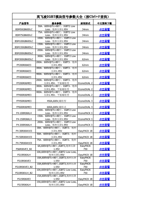
EasyPACK 750 EasyPACK 750 EasyPACK 750 EasyPACK 1B EasyPACK 1B EasyPACK 1B EasyPACK 750 EasyPACK 750 EasyPACK 750 EconoPACK 2B EasyPACK 1B EasyPACK 1B EasyPACK 1B EasyPACK 1B EasyPACK 750 EconoPACK 2B EconoPACK 2B EasyPACK 1B EasyPACK 1B EconoPACK 2B EconoPACK 2B EconoPACK 2B EconoPACK 2B EconoPACK 2B EconoPACK 2B EconoPACK 2B EconoPACK 3B EconoPACK 3B EconoPACK 3B
点击查看 点击查看 点击查看 点击查看 点击查看 点击查看 点击查看 点击查看 点击查看 点击查看 点击查看 点击查看 点击查看 点击查看 点击查看 点击查看 点击查看 点击查看 点击查看 点击查看 点击查看 点击查看 点击查看 点击查看 点击查看 点击查看 点击查看 点击查看 点击查看
FS150R06KE3 FS150R06KE3_B4 BSM200GD60DLC FS200R06KE3 FS400R06A1E3 FS400R07A1E3 FS800R06A2E3 FS800R07A2E3 FS200R07N3E4R FS200R07N3E4R_B1 1 FP50R06W2E3 BSM10GP60 BSM15GP60 BSM20GP60 BSM30GP60 BSM50GP60 BSM50GP60G BSM75GP60 BSM100GP60 FP10R06KL4 FB10R06KL4G FB15R06KL4 FB15R06KL4B1 FB20R06KL4 FB20R06KL4_B1 FP10R06KL4_B3 FP10R06W1E3 FP10R06YE3 FP10R06YE3_B4
VSC8502 评估板用户指南说明书

VSC8502User Guide VSC8502 Evaluation BoardJanuary 2019Contents1Revision History (1)1.1Revision 1.1 (1)1.2Revision 1.0 (1)2Introduction (2)3General Description (4)3.1Key Features (4)3.1.1Copper Port RJ45 Connections (4)3.1.2External RefClk Option (6)3.1.3Recovered Clocks (6)3.1.4GMII loopback card (7)3.2Key Features (7)3.2.1Single 3.3 V Input for Both DUT and Other Components (8)3.2.2DUT On-chip Regulator Power (8)4Quick Start (9)4.1Connecting the Power Supply (9)4.2PC Software Installation (9)4.3Connecting to the Board to the PC (9)4.3.1Board Initialization (10)4.3.2Copper Media Operation (Auto-negotiation Enabled) (10)4.3.3Driving Recovered Clock Output (11)4.4Useful Test Features (11)4.4.1Ethernet Packet Generator (11)4.4.2Copper PHY Error Counters (11)4.4.3Near-End Loopback (11)4.4.4Far-End Loopback (12)1Revision HistoryThe revision history describes the changes that were implemented in this document. The changes arelisted by revision, starting with the most current publication.1.1Revision 1.1Revision 1.1 of this datasheet was published in January 2019. The new Microchip template was added tothe document.1.2Revision 1.0Revision 1.0 of this datasheet was published in May 2014. This was the first publication of thedocument.2IntroductionThe VSC8502 device is a low-power, cost-optimized, dual-port gigabit Ethernet PHY. It featuresintegrated, line-side termination to conserve board space, lower EMI, and improved systemperformance. To further reduce system complexity, component count, and system cost, the VSC8502device can operate from a single 3.3 V supply using integrated voltage regulators. Additionally,integrated RGMII timing compensation eliminates the need for on-board delay lines. The device alsooptimizes power consumption in all link operating speeds and features Wake-on-LAN (WOL) powermanagement using magic packets.This document describes the architecture and usage of the VSC8502 Evaluation Board (VSC8502EV). TheQuick Start section describes how to install and run the graphical user interface (GUI) to fully control theevaluation board.Figure 1 • VSC8514 Evaluation Board (Top View)The following illustration shows the bottom view of the VSC8502 evaluation board.Figure 2 • VSC8514 Evaluation Board (Bottom View)Additional VSC8502 collateral for both the VSC8502 device and VSC8502EV, including schematics, layout, GUI, and application notes can be found on the VSC8502 producthttps:///products/product.php?number=VSC8502web page at: .3General DescriptionThe evaluation board, shown in Figure 1, provides the user a way to evaluate the VSC8502 device inmultiple configurations. Two RJ-45 connectors are provided for copper media interfaces. The MACinterface is exposed via SAMTEC connector (J1) that allows for the complete eval board to be matedwith a motherboard having the necessary signals for operating the device.For standalone access to all of the features of the device, an external microcontroller is used toconfigure the VSC8502 via the MDIO bus. The GUI enables the user to read and write device registers.3.1Key FeaturesThis section shows the key features for VSC8502.3.1.1Copper Port RJ45 ConnectionsPHY ports 0 and 1 use generic RJ45 connectors with discrete pulse H5008NL magnetics.GMII MAC ConnectorThe parallel MAC interface is available through a Samtec connector J1. As described in section 2.1.7, itcan be configured with the companion daughtercard installed at J1 aseither single-port loopback or port-port traffic passing modes.Switch Block ControlSee Figure 3 for definition of SW1 controls.See Figure 4 for the default settings.Table 1 • DIP Switch 1 OptionsDUT Control Signal DIP SW1pos ’1’ = pull up to VDDMAC; pos ‘0’ = pull down to GNDREFCLK_SEL SW1.10=125 MHz (default); 1 =25 MHzREGEN_10SW1.20=OFF (default); 1= ONREGEN_25SW1.30=OFF (default); 1= ONRESERVED3/CLK_SQUELCH_IN SW1.41=enabled(default); 0 = disabledNRESET SW1.51=operational (default); 0=held in resetCOMA_MODE SW1.60=disabled (default); 1=enabledThe following image shows the SW1 switch control for the VSC8502EV.Figure 3 • SW1 Switch ControlThe following table shows the DIP switch options for the VSC8502 evaluation board.Table 2 • DIP Switch 2 OptionsDUT Control Signal DIP SW1pos ’1’ = pull up to VDDMAC; pos ‘0’ = pull down to GNDRCVRDCLK1/PHYADD1SW1.10=defaultRCVRDCLK2/PHYADD2SW1.20=defaultPHYADD3SW1.30=defaultPHYADD4SW1.40=defaultNote: R17 and R18 0 ohm options must be installed for PHYADD1 and PHYADD2 to be affected by SW2, otherwise they are internally pulled to GND. Also, PHYADD3-4 pinsare internal PD on the VSC8502 IC, and are weakly pulled to GND when their corresponding SW2 pins are kept in ‘0’ position.Figure 4 • SW2 Switch Control3.1.2External RefClk OptionThe user may choose to provide an external PHY REFCLK via SMA connection to J8 (as shown in Figure1). To route the SMA signal to the device the user must reorient thezero ohm resistor R25, as shown from the PCB layout view in Figure 7.Note: external PHY REFCLK must be connected via SMA to J8 if 3.3 V VDDIO/VDDMAC is used, since theon-board crystal oscillator (U5) is a 2.5 V CMOS driver.R25 can also be connected across pins 1 and 2 if a user wants to provide DUT REFCLK input from theSamtec connector J1.Figure 5 • REFCLK Input Options - R25 3-Way Orientation3.1.3Recovered ClocksThere are two recovered clocks available from the VSC8502, through SMA connections J5 (RCVRDCLK1)and J6 (RCVRDCLK2). In the default configuration, CLK_SQUELCH_INis pulled down, which disables the clock squelching and RCVRDCLK1/RCVRDCLK2 are connected to theSamtech header J1. To route RCVRDCLK1 and RCVRDCLK2 to SMAsJ5 and J6, reorient zero ohm resistors R21 and R23, respectively.Software Interface Microcontroller CardA Silabs F340 microcontroller is included to facilitate a software interface to the registers on theVSC8502 through a USB port.Note: Alternatively, a Rabbit card is available for an IP-based manager of the PHY register space,installed in the keep-out area (U6) of the board’s top-side. Or, MDCand MDIO can be accessed on stake header J10 if desired for another microcontroller to host the PHYregister space.3.1.4GMII loopback cardThe VSC8502EV ships with a daughter card that mounts to J1 to loop-back the GMII/RGMII interface.As shown in Figure 8 and Figure 9 below, one orientation of the loopback card will loop each port backto itself (IN-CHANNEL LOOPBACK in Figure 8). The other orientationforwards bidirectional traffic from one port to the other (CHANNEL TO CHANNEL LOOPBACK).Figure 6 • Loopback Card (Side A)Figure 7 • Loopback Card (Side B)Note: this daughter card loopback only supports 1000 BASE-T in GMII mode and 10/100/1000 in RGMIImode. It will not support 10/100 in MII mode.However, there are other internal loopback modes that will support BER testing of MII mode such as far-end loopback (MII Register 23.3).3.2Key FeaturesThis section shows the power supply options for VSC8502.3.2.1Single 3.3 V Input for Both DUT and Other ComponentsThis option allows for one external 3.3 V supply connected to J11 to power everything on the board. Usethe following steps:SW1 REGEN1V0 = REGEN2V5 = 0: disable on-chip regulatorsInsert a 3.3 V DC supply (rated for 1 Amp) into J11Unplug banana connectors J16(+): J17(GND)Unplug banana connectors J19(+): J20(GND)Populate J23: 3V3_DUT = 3V3_MAINPopulate J15: 2V5_DUT = 2V5Populate J26: VDD25A = 2V5_DUTRemove J18: on-board 3.3 V to 2.5 V regulator enabledPopulate J25: VDD1 = 1V0Remove J12: on-board 3.3 V to 1.0 V regulator enabledPopulate J24: VDDMAC = 3V3_DUT or 2V5_DUT (VDDMAC is tied to VDDIO. The DUT’s VDDIO canoperate at either 2.5 V or 3.3 V)Populate J9: VDDMDIO = VDDIO (1.2 V option is not available at this time, due to inability to drive1.2 V from on-board microcontroller options)DUT Power Rails Isolated from non-DUT PowerThis option allows for the DUT power supplies to be isolated from the rest of the board power. Use thefollowing steps:SW1 REGEN1V0 = REGEN2V5 = 0: disable on-chip regulatorsInsert a 3.3 V DC supply (rated for 1 Amp) into J11Populate banana jacks J13(+): J14(GND) with 3.3 V supplyPopulate banana jacks J16(+): J17(GND) with 2.5 V supplyPopulate banana jacks J19(+): J20(GND) with 1.0 V supplyRemove J23: 3V3_DUT = J13 (3.3 V)Remove J15: 2V5_DUT = J16 (2.5 V)Populate J26: VDD25A = 2V5_DUTRemove J18: on-board 3.3 V to 2.5 V regulator enabledPopulate J25: VDD1 = 1V0 (note: 1V0 = J19)Populate J12: on-board 3.3 V to 1.0 V regulator disabledPopulate J24: VDDMAC = 3V3_DUT or 2V5_DUT (VDDMAC is tied to VDDIO. The DUT’s VDDIO canoperate at either 2.5 V or 3.3 V)Populate J9: VDDMDIO = VDDIO (1.2 V option is not available at this time, due to inability to drive1.2 V from on-board microcontroller options)3.2.2DUT On-chip Regulator PowerThe on-chip regulator option for this board is for engineering purposes only. There are performanceissues associated with using the on-chip regulator on this board, so it isan unsupported board feature.1. 2. 3. 4. 4Quick StartThis section shows the quick start for VSC8502.4.1Connecting the Power SupplyThe evaluation board offers choices of how to power the 3.3 V, 2.5 V, and 1.0 V rails which drive the devices as well as modules; please see section 2.2 for reference. The simplest power option for theevaluation board is to use the power pack for 3.3 VDC. Simply plug the AC adaptor into a wall socket and the barrel end into J11 (see the upper left corner of Figure 1). Immediately the user should see several LEDs turn on.Note: for proper power-on sequencing on this board, please toggle NRESET input to the DUT using either SW3 (push-button) or SW1 (DIP) after board power is applied but prior to launching the GUI.4.2PC Software InstallationDownload the ZIP file from Vitesse’s website onto a PC that has a USB port Install the GUI by launching the setup.exe fileUSB communication is assisted by the Silabs USBXpress® drive. If not present on the PC, the user will need to download theUSBXpress development kit from the Silicon Labs website (URL: /products )/mcu/Pages/USBXpress.aspx Double click the desktop icon to launch the GUI4.3Connecting to the Board to the PCLaunch the GUI either by clicking on the desktop shortcut or clicking on the “Star t> Programs > Vitesse Semiconductor Corp > VSC8502_GUI” icon. The initial window will detect the attached USB devices automatically. Figure 10 shows a typical EVB Connection window.Figure 8 • GUI Connection WindowThe EVB serial number should appear. If not, click on “Scan For USB Devices.” Select that EVB serial number then click “Launch GUI”. The Register List window will appear as shown in Figure 11.Figure 9 • MII Registers GUI WindowBe sure the device is up and running by reading MII Register 0. It should read back 0 × 1040. Readingback all 0’s or all 1’s indicates a problem. For a multi-port device, the corresponding PHY port number isaccessed via the “Port:” pick list shown above the Register Description in Figure 11.As Figure 11 indicates, the extended MII register pages can be accessed to read or write by clicking onone of the ExtMII/Ext2MII/ExtGMII tabs.4.3.1Board InitializationNote: if J1 is used for an evaluation session, the SAMTEC connector J1 should be populated prior topower-on of the board (for example, with the companion GMII loopback card show in section 2.1.7 for adesired external loopback mode). Once the evaluation board connectivity has been established andconfirmed, the PHY should be initialized. Initialization can be accomplished by running an init-scriptsequence, such as performed by the pre- and post-reset functions of the PHY API standalone app.While the init-script sequence may not be required for specific operational modes, an init-scriptsequence is highly recommended to ensure correct performance over the greatest set of user scenariosfor the PHY. After initialization is performed, refer to the PHY Datasheet section on configuring the PHYand PHY Interfaces for the desired application.4.3.2Copper Media Operation (Auto-negotiation Enabled)The easiest configuration for passing traffic is with Autoneg enabled (MII 0 bit 12 = 1). Use MII Register0, 4 and 9 to change speed and restart autoneg (MII 0 bit 9) to advertise new settings. As per thedatasheet descriptions, the commonly-used speed advertisement definitions are as follows:Table 3 • Auto-Negotiation Advertisements1. 2. 3. 4.MII reg 4bits 8:7MII reg 4bits 6:5MII reg 9bits 12:11MII reg 9bits 9:81000BT Master mode N/A N/A 11111000BT Slave mode N/A N/A 1011100 BASE-TX Full Duplex 11N/A N/A 0010 BASE-T Full Duplex0011N/A00The following steps are used to configure a link:Set up the Copper traffic source (i.e., IXIA or Smartbits)Connect Ethernet cable(s) to a single or multiple RJ-45 portsConfigure auto-negotiation as per above and re-start ANEG (MII bit 0.12)The linkup bit is in MII Reg 1, bit 2 (MII 1.2), read it twice to update Traffic should now be flowing.4.3.3Driving Recovered Clock OutputTo output the a recovered clock from the PHY on this evaluation board, ensure zeroohm resistors R21 and R23 are oriented as per section 2.1.5 and perform the following register writes to enable RCVRDCLK1 with PHY0 as the clock source:Write 0×8101 to register 23 of the “General Purpose Registers” when PHY0’s link is up in a non-EEE mode and not 1000BT master or 10BTSet MII Register bit 9.12 to enable manual slave configuration then issue an auto negotiation restart through register bit 0.9To select a different port as the clock source or enable a recovered clock for EEE mode, refer to register 23 G/24 G in the datasheet for the programming detail.Note: The recovered clock output is intended to drive a CMOS load, not a DCcoupled low impedance such as a scope 50-Ohm termination. The recommended measurement equipment is an active (high-impedance) differential probe. Refer to the device datasheet for additional loading and performance specifications.4.4Useful Test Features4.4.1Ethernet Packet GeneratorExtMII 29E is the Ethernet Packet Generator register. The EPG sends traffic in multiple of 10,000 frames regardless of when you stop transmit activity. Refer to the datasheet for configuration options.A good CRC packet counter is in ExtMII 18.13:0. The good CRC packet counter is a modulo 10,000 counter so values will always be between 0-9,999. A read of the register reads back the good CRCpackets and then clears the register so the subsequent reads will be 0 if no traffic has been received. If traffic has been received since the last read, bit 15 will be set.4.4.2Copper PHY Error CountersIdle errors = MII 10.7:0RX errors = MII 19.7:0False carrier = MII 20.7:0Disconnects = MII 21.7:0CRC errors = ExtMII 23.7:04.4.3Near-End LoopbackWhen the near-end loopback test feature is enabled, the transmitted data is looped back in the PCS block on the receive data signals. To enable the loopback, set register bit 0.14 to 1. Near-end loopback mode involves traffic flow over the GMII/RGMII interface, so a breakout of the MAC interface on SAMTEC connector J1 must be connected to another system for this mode to pass traffic.SAMTEC connector J1 must be connected to another system for this mode to pass traffic.4.4.4Far-End LoopbackWhen the far-end loopback test feature is enabled, incoming data from a link partner on the Copperinterface to be transmitted back to the link partner on the Copper interface. To enable the loopback, setregister bit 23.3 to 1.Microsemi HeadquartersOne Enterprise, Aliso Viejo,CA 92656 USAWithin the USA: +1 (800) 713-4113Outside the USA: +1 (949) 380-6100Sales: +1 (949) 380-6136Fax: +1 (949) 215-4996Email:***************************© Microsemi. All rights reserved. Microsemi and the Microsemi logo are trademarks of Microsemi Corporation. All other trademarks and service marks are the property of their respective owners.Microsemi makes no warranty, representation, or guarantee regarding the information contained herein or the suitability of its products and services for any particular purpose, nor does Microsemi assume any liability whatsoever arising out of the application or use of any product or circuit. The products sold hereunder and any other products sold by Microsemi have been subject to limited testing and should not be used in conjunction with mission-critical equipment or applications. Any performance specifications are believed to be reliable but are not verified, and Buyer must conduct and complete all performance and other testing of the products, alone and together with, or installed in, any end-products. Buyer shall not rely on any data and performance specifications or parameters provided by Microsemi. It is the Buyer's responsibility to independently determine suitability of any products and to test and verify the same. The information provided by Microsemi hereunder is provided "as is, where is" and with all faults, and the entire risk associated with such information is entirely with the Buyer. Microsemi does not grant, explicitly or implicitly, to any party any patent rights, licenses, or any other IP rights, whether with regard to such information itself or anything described by such information. Information provided in this document is proprietary to Microsemi, and Microsemi reserves the right to make any changes to the information in this document or to any products and services at any time without notice.Microsemi, a wholly owned subsidiary of Microchip Technology Inc. (Nasdaq: MCHP), offers a comprehensive portfolio of semiconductor and system solutions for aerospace & defense, communications, data center and industrial markets. Products include high-performance and radiation-hardened analog mixed-signal integrated circuits, FPGAs, SoCs and ASICs; power management products; timing and synchronization devices and precise time solutions, setting the world's standard for time; voice processing devices; RF solutions; discrete components; enterprise storage and communication solutions; security technologies and scalable anti-tamper products; Ethernet solutions; Power-over-Ethernet ICs and midspans; as well as custom design capabilities and services. Microsemi is headquartered in Aliso Viejo, California, and has approximately 4,800 employees globally. Learn more at www. .VPPD-03741。
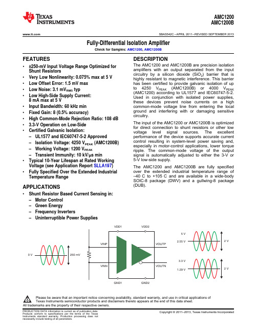
AMC1200中文资料_数据手册_参数
2
PRODUCTION DATA information is current as of publication date. Products conform to specifications per the terms of the Texas Instruments standard warranty. Production processing does not necessarily include testing of all parameters.
1
•2 ±250-mV Input Voltage Range Optimized for Shunt Resistors
• Very Low Nonlinearity: 0.075% max at 5 V • Low Offset Error: 1.5 mV max • Low Noise: 3.1 mVRMS typ • Low High-Side Supply Current:
Copyright © 2011–2013, Texas Instruments Incorporated
AMC1200 AMC1200B
SBAS542C – APRIL 2011 – REVISED SEPTEMBER 2013
This integrated circuit can be damaged by ESD. Texas Instruments recommends that all integrated circuits be handled with appropriate precautions. Failure to observe proper handling and installation procedures can cause damage.
DVCC-DEK 使用说明
目录第一章 DVCC-DEK 实验平台硬件组成 (2)1.1供电电源 (2)1.1.1供电总电源 (2)1.1.2系统板工作电源 (2)1.1.3 实验模块供电电源 (2)1.2系统板组成 (2)1.2.1 供电电源 (2)1.2.2 一路模拟电压产生电路 (2)1.2.3 2路手动±单脉冲 (2)1.2.4 固定脉冲发生电路 (3)1.2.5 开关量输入显示 (3)1.2.6 开关量输出并显示 (4)1.2.7 独立复位输出电路 (4)1.2.8 2位数码管BCD译码显示电路 (4)1.2.9 一个扩展插座 (5)第二章独立实验模块介绍 (6)2.1模块配置简要说明 (6)2.2模块编号的说明 (6)2.3模块上插头座的功能和使用 (6)2.3.1 电源插座 (6)2.3.2 数据总线插座 (6)2.3.3 其它信号线插孔 (6)2.3.4 模块编号的说明 (6)2.4本系统配置的各实验模块原理图、布局图和简单说明 (6)2.4.1 1号模块: A/D和D/A转换(数模/模数转换) (6)2.4.2 2号模块:机电一体化模块(步进电机、直流电机、继电器、音频放大) (8)2.4.3 38号模块:4×4矩阵键盘和8位数码管 (9)2.4.4 17号模块: RS232/RS485/USB通信/串行A/D/D/A/看门狗/数字温度传感器 (9)2.4.5 18号模块:串行键盘控制ZLG7290、I2C电路(IC卡)电路 (11)2.4.6 19号模块:CAN 总线通信、无线红外通信 (11)2.4.7 9_1号模块:16×2液晶显示、128×64液晶显示、实时时钟DS1302 (12)2.4.8 20号模块:以太网通信模块 (13)2.4.9 高速AD、串行AD、DA 综合模块 (15)2.4.10 DDS信号发生器模块 (16)2.4.11 温度测量控制模块 (17)2.4.12 16x16点阵控制模块 (18)2.4.13 并行I/O接口 8255A和定时/计数器8253A模块 (19)2.5 核心模块简介 (20)2.5.1 EP2C8T144 核心模块 (20)2.5.2 飞思卡尔MC9S12SX256核心模块 (21)2.5.3 STM32 ARM核心模块 (22)2.5.4 51单片机核心模块 (23)第一章 DVCC-DEK 实验平台硬件组成由供电电源、系统板、模块化实验板、单片机核心板等组成。
FAN4800设计的300W高效LED电源
5. Boost Inductor (L2)
5.1. Winding Specification
No
Pin (S - F)
N1
1Æ2
Core: Toroid core (CM270060)
Wire 0.8Ф
Turns 117Ts
Winding Method
3
RD-268_FAN4800A • Rev. 0.0.1
2. Flyback Converter Transformer (TX1)
Figure 3. Transformer Schematic Diagram
2.1. Winding Specification
6.1. Winding Specification
No
Pin (S - F)
N1
3Æ8
N2
4Æ7
N3
1Æ10
N4
2Æ9
N5
5Æ6
Wire 1.0Ф 1.0Ф 1.0Ф 1.0Ф 0.5Ф
Core: Toroid Optimag Magnetic HF106060-2
ห้องสมุดไป่ตู้
6.2. Electrical Characteristics
© 2009 Fairchild Semiconductor Corporation
2
RD-268_FAN4800A • Rev. 0.0.1
Figure 2. Schematic of Main Power Stage (FAN4800A)
© 2009 Fairchild Semiconductor Corporation
0.4Ф
N5
2-6,7
BIT3252A 升压型LED背光驱动器 高频PWM控制器
BIT3252ALow Cost PWM Controllerbuilt in55V NMOSVersion: A2Please read the notice stated in this preamble carefully before accessing any contents of the document attached.Admission of BiTEK’s statement therein is presumed once the document is released to the receiver.Notice:Firstly, the information furnished by Beyond Innovation Technology Co. Ltd. (BiTEK) in this document is believed to be accurate and reliable and subject to BiTEK’s amendment without prior notice. And the aforesaid information does not form any part or parts of any quotation or contract between BiTEK and the information receiver.Further, no responsibility is assumed for the usage of the aforesaid information. BiTEK makes no representation that the interconnect of its circuits as described herein will not infringe on exiting or future patent rights, nor do the descriptions contained herein imply the granting of licenses to make, use or sell equipment constructed in accordance therewith.Besides, the product in this document is not designed for use in life support appliances, devices, or systems where malfunction of this product can reasonably be expected to result in personal injury. BiTEK customers’ using or selling this product for use in such applications shall do so at their own risk and agree to fully indemnify BiTEK for any damage resulting from such improper use or sale.At last, the information furnished in this document is the property of BiTEK and shall be treated as highly confidentiality; any kind of distribution, disclosure, copying, transformation or use of whole or parts of this document without duly authorization from BiTEK by prior written consent is strictly prohibited. The receiver shall fully compensate BiTEK without any reservation for any losses thereof due to its violation of BiTEK’s confidential request. The receiver is deemed to agree on BiTEK’s confidential request therein suppose that said receiver receives this document without making any expressly opposition. In the condition that aforesaid opposition is made, the receiver shall return this document to BiTEK immediately without any delay. -Version A4y Array y y y y y y y yyLayout Notice:Some of the pins are very sensitive to noise. Please follow the bellowing guideline to make the layout:Soldering InformationReflow Soldering:The choice of heating method may be influenced by plastic QFP package). If infrared or vapor phase heating is used and the package is not absolutely dry (less than 0.1% moisture content by weight), vaporization of the small≧Unit: mm SOP type :。
BL8034 1 4A, 16V高效同步步下转换器说明书
4A, 16V High Efficiency Synchronous Step-Down ConverterBL8034DESCRIPTIONThe BL8034 is a wide input range, high-efficiency, DC-to- DC step-down switching regulator, capable of delivering up to 4A of output current. Current mode PWM control allows the use of small external components, such as ceramic input and output caps, as well as small inductors, while still providing low output ripples. On top of the integrated internal synchronous rectifier that eliminates external Schottky diode, BL8034 also employs a proprietary control scheme that switches the device into a power save mode during light load, thereby extending the range of high efficiency operation. Therefore, BL8034 is a much superior solution in comparison to other competitions in terms of efficiency and cost. Overall, BL8034 is a highly efficient and robust solution for DC-DC step-down applications that requires wide input ranges.The BL8034 is available in ESOP8 package. FEATURES∙ Wide Input Operating Range from 4.2V to 16V ∙ High Efficiency: Up to 95% at Light Load ∙ Capable of Delivering 4A∙ No external Schottky Diode Needed ∙ Inductor Short Circuit Protection ∙ Current Mode Control∙ 0.923V Reference for Low Output Voltages ∙ Logic Control Shutdown∙ Thermal Shutdown and UVLO ∙ Available inESOP8 PackageAPPLICATIONS∙ LCD TVs∙ Notebook computers ∙ FPGA power supplies ∙ LED driversTYPICAL APPLICATIONC3MARK and PIN OUTESOP8ORDERING INFORMATIONPINOUT DESCRIPTIONABSOLUTE MAXIMUM RATINGNote:Exceed these limits to damage to the device. Exposure to absolute maximum rating conditions may affect device reliability.ELECTRICAL CHARACTERISTICSTYPICAL PERFORMANCE CHARACTERISTICS (L=4.7uH, Cin=22uF, Cout=22uF, T A=25 C, unless otherwise stated)FUNCTIONAL DECRIPTIONSLoop OperationThe BL8034 is a wide input range, high-efficiency, DC-to-DC step-down switching regulator, capable of delivering up to 4A of output current, integrated with a 120/60m synchronous MOSFET pair, eliminating the need for external diode. It uses a PWM current-modecontrol scheme. An error amplifier integrates error between the FB signal and the internal reference voltage. The output of the integrator is then compared to the sum of a current-sense signal and the slope compensation ramp. This operation generates a PWM signal that modulates the duty cycle of the power MOSFETs to achieve regulation for output voltage.Current LimitThere is a cycle-by-cycle current limit on the high-side MOSFET of 6A(typ). When the current flowing out of SW exceeds this limit, the high-side MOSFET turns off and the synchronous rectifier turns on. Unlike the traditional method of current limiting by limiting the voltage at the compensation pin, which usually has large variation due to duty cycle variance, this type of peak current limiting scheme provides a relatively more accurate limit for output current, thereby lowering the requirements for system design.Light Load OperationTraditionally, a fixed constant frequency PWM DC-DC regulator always switches even when the output load is small. When energy is shuffling back and forth through the power MOSFETs, power is lost due to the finite RDSONs of the MOSFETs and parasitic capacitances. At light load, this loss is prominent and efficiency is therefore very low. BL8034 employs a proprietary control scheme that improves efficiency in this situation by enabling the device into a power save mode duringlight load, thereby extending the range of high efficiency operation.PCB LAYOUT RECOMMENDATIONThe device’s performance and stability are dramatically affected by PCB layout. It is recommended to follow these general guidelines shown as below:1. Place the input capacitors and output capacitors as close to the device as possible. The traces which connect to these capacitors should be as short and wide as possible to minimize parasitic inductance and resistance.2. Place feedback resistors close to the FB pin.3. Keep the sensitive signal (FB) away from the switching signal (SW).4. The exposed pad of the package should be soldered to an equivalent area of metal on the PCB. This area should connect to the GND plane and have multiple via connections to the back of the PCB as well as connections to intermediate PCB layers. The GND plane area connecting to the exposed pad should be maximized to improve thermal performance.5. Multi-layer PCB design is recommended.PACKAGE OUTLINE。
SP4502
负载插入时 SP4502 可以自动检测到负载并开启升压电 路工作。当负载拔掉,经过 16S 延时,升压电路关闭, IC 进入低电流待机模式。
放电指示
放电时,LED1~LED4 根据电池电压指示当前电量,当 电池电压低于 3.05V 时,LED1 会以 2HZ 频率快闪进行 低电提示。
单位 V V A A ℃ ℃ V V
符号 VDD
IC TOP
参数 充电输入电压 充电电流 工作环境温度
参数范围 4.5~5.5
≤2 -20~85
单位 V A ℃
注 1:最大极限值是指超出该工作范围芯片可能会损坏。推荐工作范围是指在该范围内芯片工作正常,但不完全保证满足 个别性能指标。电气参数定义了器件在工作范围内并且在保证特定性能指标的测试条件下的直流和交流电气参数规范。对 于未给定的上下限参数,该规范不予保证其精度,但其典型值合理反映了器件性能。
测试条件
针对 4.2V 规格 针对 4.35V 规格 VBAT-VRECHRG RISET=75Ω,恒流充电模式 RISET=75Ω,涓流充电模式 RISET=75Ω RISET=75Ω,VBAT 上升 RISET=75Ω
VBAT 上升 VBAT 下降
VBAT=3.7V VDD 上升 VDD 下降 ILOAD=1A,VBAT=3.7V 温度上升
概述
SP4502 是一款专为移动电源设计的同步开关充电和同步 升压的单芯片解决方案,内部集成了同步开关充电模块、同 步升压放电管理模块、电量检测与 LED 指示模块、保护模 块。 SP4502 内置充电与放电功率 MOS,充电电流可以设定, 最大充电电流为 2.5A,同步升压输出为 2.1A。 SP4502 采用专利的充电电流自适应技术以适应小电流适 配器,同时采用专利的控制方式省去外部的功率设定电阻, 降低功耗的同时降低系统成本。 SP4502 内部集成了温度补偿、过温保护、过充与过放保护、 输出过压保护、输出重载保护、输出短路保护等多重安全 保护功能以保证芯片和锂离子电池的安全,应用电路简单, 只需很少元件便可实现充电管理与放电管理。
- 1、下载文档前请自行甄别文档内容的完整性,平台不提供额外的编辑、内容补充、找答案等附加服务。
- 2、"仅部分预览"的文档,不可在线预览部分如存在完整性等问题,可反馈申请退款(可完整预览的文档不适用该条件!)。
- 3、如文档侵犯您的权益,请联系客服反馈,我们会尽快为您处理(人工客服工作时间:9:00-18:30)。
BL8542BREV1.2, DEC 20100.85V startup, 1MHz, 300mA Iout, Synchronous Boost Convert erDESCRIPTIONThe BL8542B is a step-up converter that provides a boosted output voltage from a low voltage source. Because of its proprietary design, it starts up at a very low input voltage down to 850mV, making it an ideal choice for single cell alkaline/NiMH battery operations.A switching frequency of 1MHz minimizes solution footprint by allowing the use of tiny, low profile inductors and ceramic capacitors. The current mode PWM design is internally compensated, reducing external parts count.BL8542B is housed in a tiny SOT23-5 and SOT89-3 Package.FEATURESUp to 95% Ef ficiency• Output voltage accuracy 3%• 1MHz Switching Frequency allows small inductor • and output capInput boost-strapping allows using small or no • input capLow Vin Start-up Voltage down to 850mV Ideal • for Single Alkaline Cell operationsMaximum Output Current up to 300mA • Low Noise PWM control• Internally Compensated Current Mode Control • Internal Synchronous Recti fier • Logic Control Shutdown (IQ<1uA)•APPLICATIONSOne to Three Cell Battery Operated Devices • Medical Instruments • Bluetooth Headsets• Flash-Based MP3 Players• Noise Canceling Headphones•TYPICAL APPLICATION CIRCUITNOTE: Input capacitor (Cin=0.47uF) and Output capacitor (Cout ≥4.7uF) are recommended in all application circuit.PIN CONFIGURATIONORDERING INFORMATIONProductProduct CodePackageDevices per ReelTop MarkingBL8542B-ADJ BL8542BCB5TR SOT23-53000AAXZ BL8542B-3.3V BL8542BCB5TR33SOT23-53000AAWZ BL8542B-5.0V BL8542BCB5TR50SOT23-53000AAVZBL8542B-3.3V BL8542BCC3TR33SOT89-31000AAWZ XXXX BL8542B-5.0VBL8542BCC3TR50SOT89-31000AAVZXXXXGBL8542B BL8542BBL8542BSOT23-5SOT89-3XXXX:The last 4 characters of the LOT NO.BLOCK DIAGRAMDETAIL DESCRIPTIONBL8542B is a low input voltage start up, current mode dc-dc step up converter. It’s operation can be best understood by referring to the block diagram. Upon starting up, the low voltage startup circuitry drives SW with on-off cycles, transferring energy from input to OUT by storing energy in the inductor during on-time and releasing it to the output during off-time. When OUT reaches 2V, the startup circuit turns off and the main controller takes over. The main control loop consists of a reference, a GM error amplifier, a PWM controller, a current sense amplifier, an oscillator, a PWM logic control, and it is power stage including its driver. The main control loop is a classic current mode control loop. The GM stage integrates the error between FB and REF, and its output is used to compare with a triangular wave which the summing result of the current sense amplifier output and a slope compensation voltage. The output of the comparator is used to drive the power stage to reach regulation.APPLICATION INFORMATIONOutput Voltage selectionThe output voltages can be set by connecting FB to OUT, to G or to the midpoint of a resistor divider connected to OUT. See below table for details.FB=G VOUT =5.0VFB=OUT VOUT =3.3VFB to resistor divider VOUT=0.6V(1+R1/R2)Inductor selectionWith switching frequency up to 1MHz, small surface mount inductors can be used with values from 2.2uH to 4.7uH. For a given chosen inductor value and application conditions make sure the peak inductor current does not exceed the maximum current rating of the selected vendor's inductor.Input and output capacitor selectionThe BL8542B's bootstrap architecture allows the use of very small input capacitor. For applications that only need to drive small output load current, the input capacitor is optional, because once output is started up, the IC's is powered by OUT, a quiet power supply.The output capacitor is used to stabilize the loop and provide ac current to the load. A low ESR ceramic cap with values from 2.2uF to 22uF can be used. Smaller value capacitors are generally cheaper with small footprints, while larger capacitor provides lower ripples and better transient load responses. Also, when extreme low startup voltage is needed, larger output capacitors are needed for the part to startup under heavy load condition.ABSOLUTE MAXIMUM RATINGParameters ValueSW Voltage-0.3 ~ 6 VEN, FB, OUT Voltage-0.3 ~ 6 VJuntion to Ambient Thermal Resistance190 o C/WMaximum Power Dissipation0.45 WOperating Temperature Range-40 ~ 150 o CStorage Temperature-55 ~ 150 o CIR Reflow Lead Temperature and Time260o C , 10sNote:Exceed these limits to damage to the device.Exposure to absolute maximum rating conditions may affect device reliability.ELECTRICAL CHARACTERISTICSTest condition: Vin=1.8V, Vout=3.3V, T A=25o C, unless otherwise specified.Parameters Condition Min.Typ.Max.Unit Minimum Input Voltage0.7V Startup Voltage0.85 1.1VDropout Voltage, Vout≥2.8V FB=OUT 3.3V FB=G5VFB Feedback Voltage Vout=2.5 to 5V0.6V FB Input Current50nA Output Voltage Range External divider 2.55V Quiescent Current at OUT Vfb=0.7V25uA Shutdown Supply Current at OUT EN=G0.11uA NMOS Switch On Resistance Isw=100mA0.3ohm PMOS Switch On Resistance Isw=100mA0.7ohm NMOS Switch Current Limit1ASW Leakage Current Vout=5.5V, Vsw=0 or 5.5V,EN=G1uA EN Input Current1uA EN Input Voltage for “Low”0.3V EN Input Voltage for “High”0.6VTypical values are tested at T A=25o C, unless otherwise specified.Typical values are tested at T A=25o C, unless otherwise specified.PACKAGE OUTLINE DIMENSIONPackage SOT23-5Devices per reel3000 Dimension (mm)Package SOT89-3Devices per reel1000Dimension (mm)。